
Sb2S3-Based Dynamically Tuned Color Filter Array via Genetic Algorithm

 and
and
Abstract
:1. Introduction
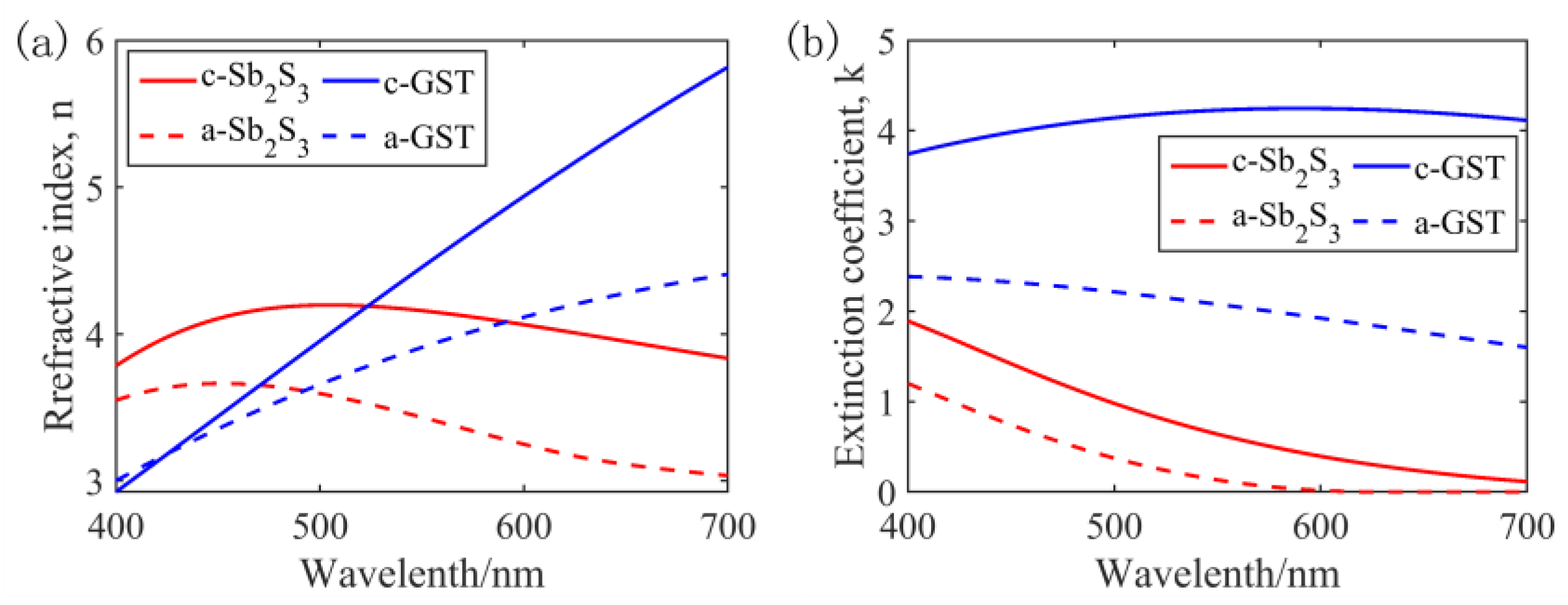
2. Methods
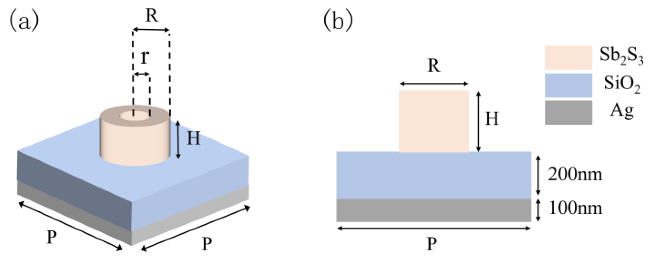
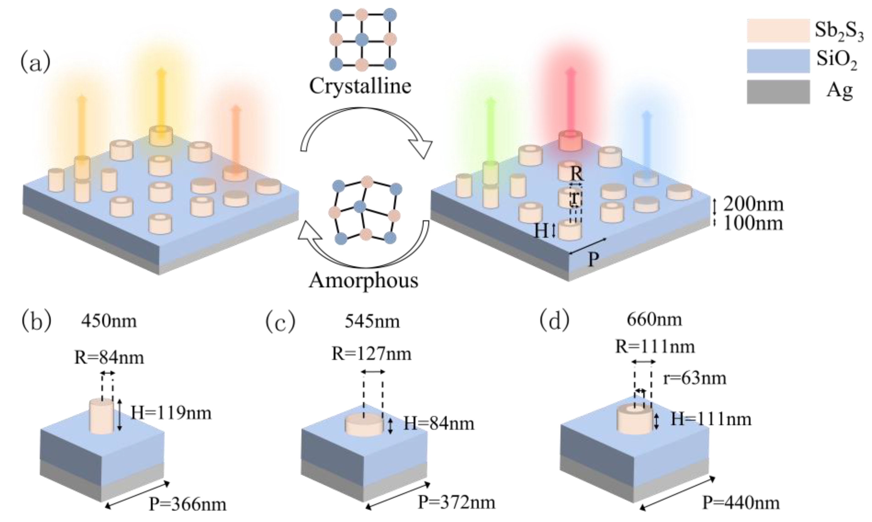
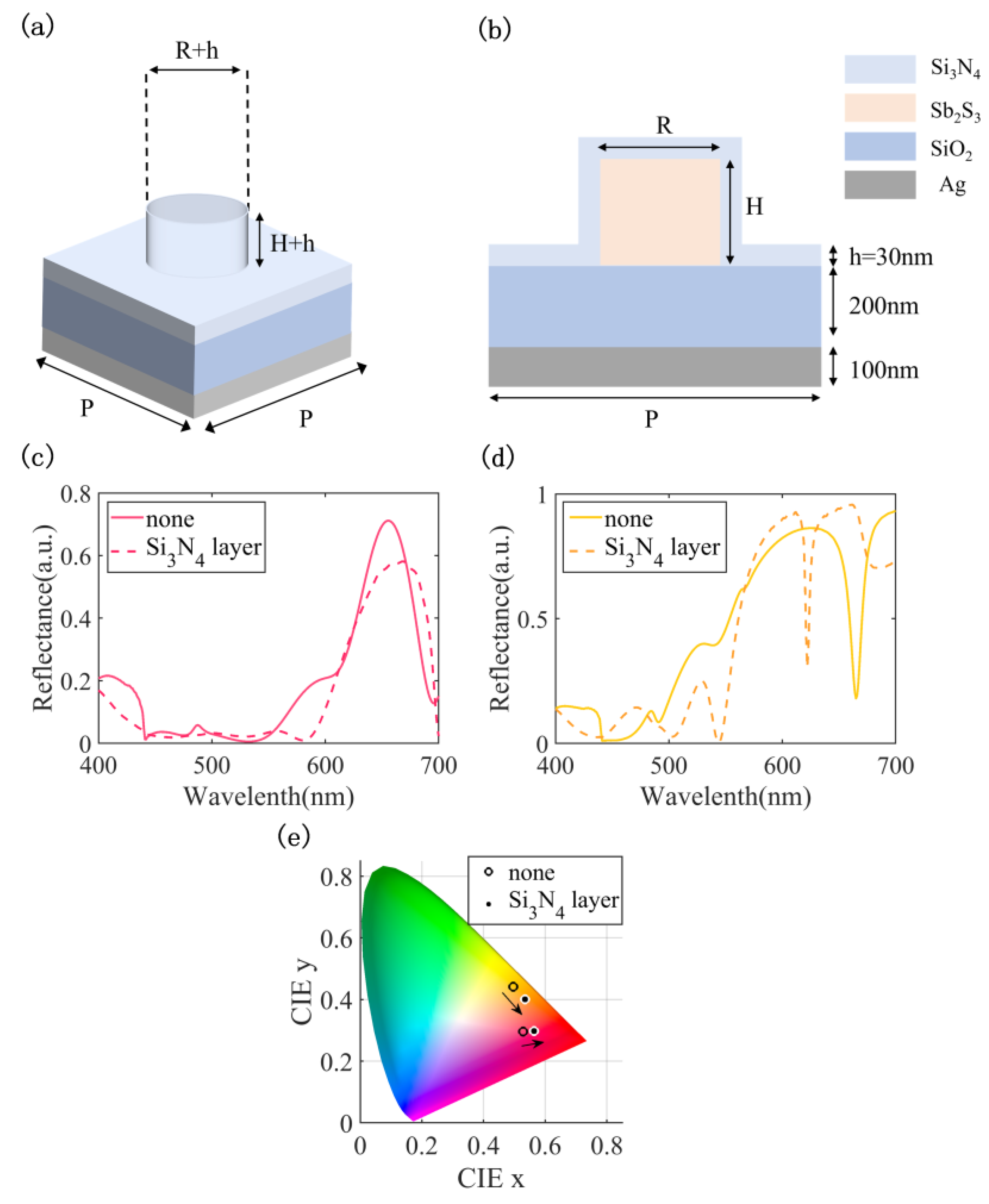
2.1. Metasurface Structure
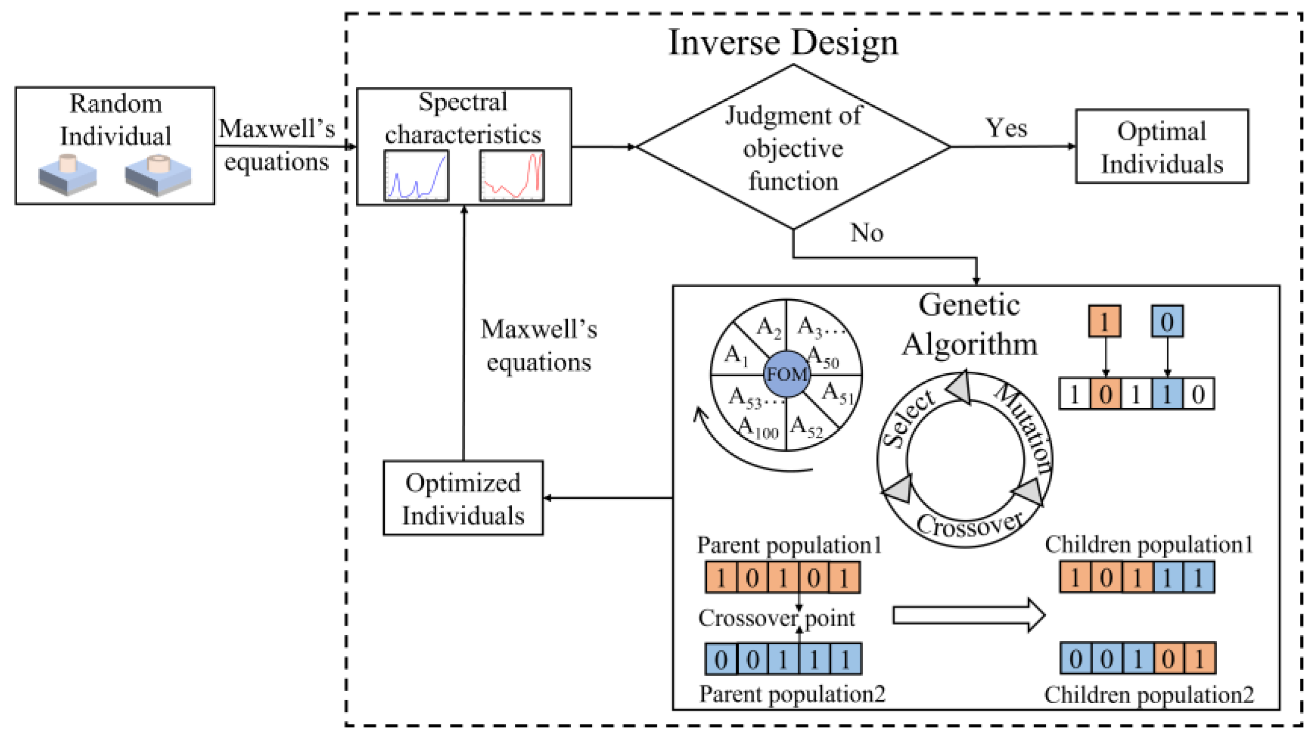
2.2. Process of Inverse Design
2.3. Color Calculation
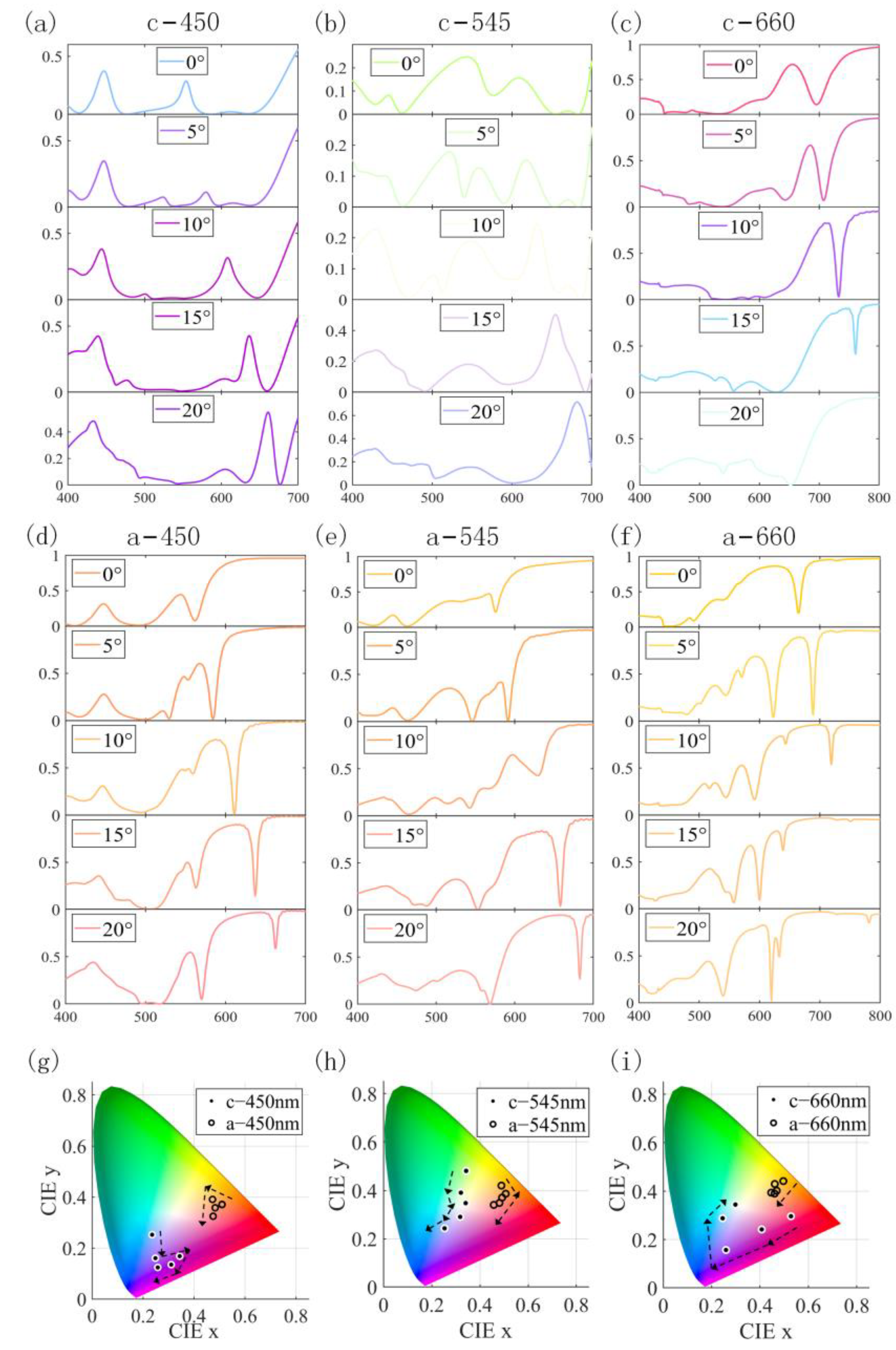
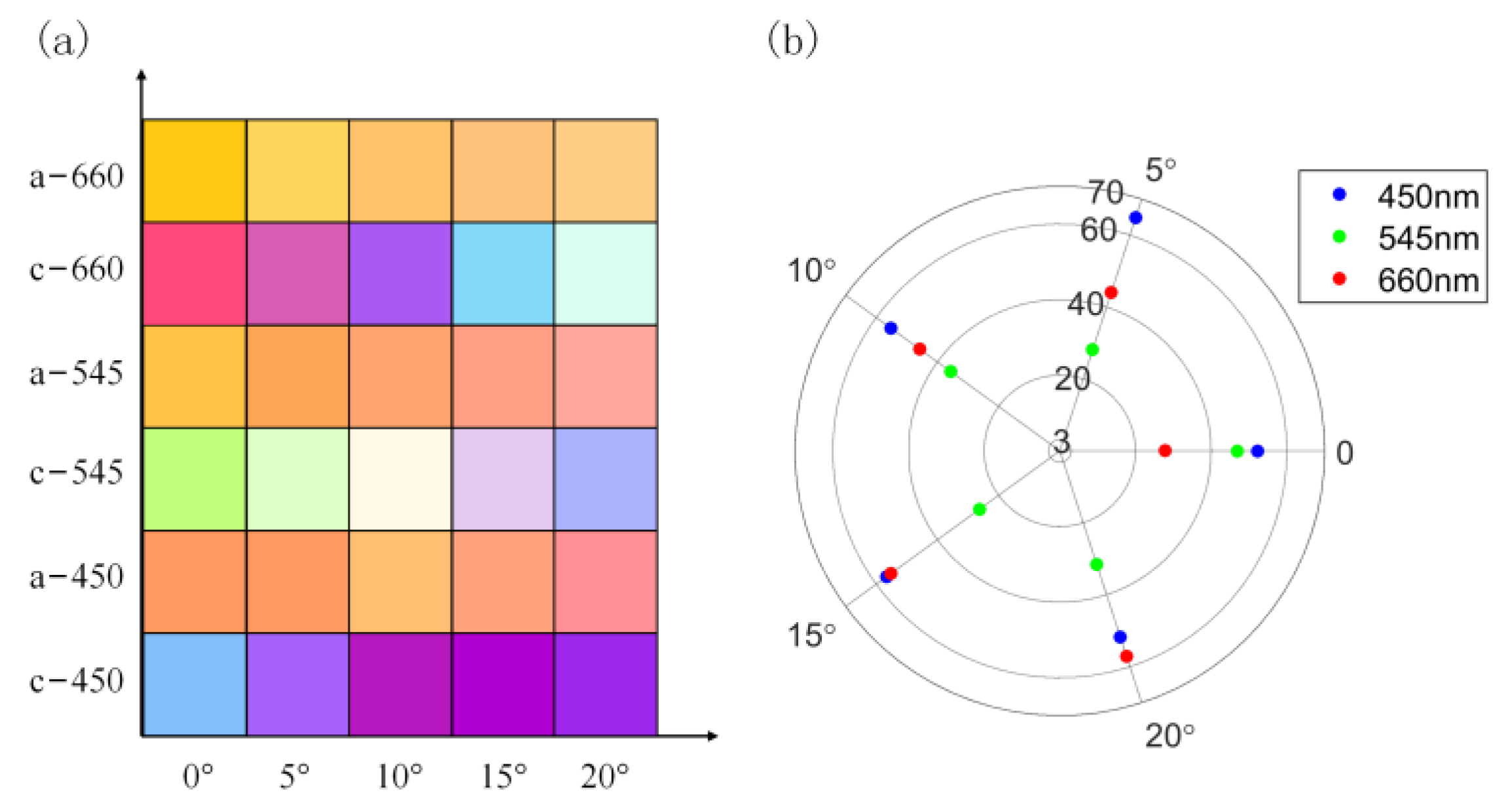
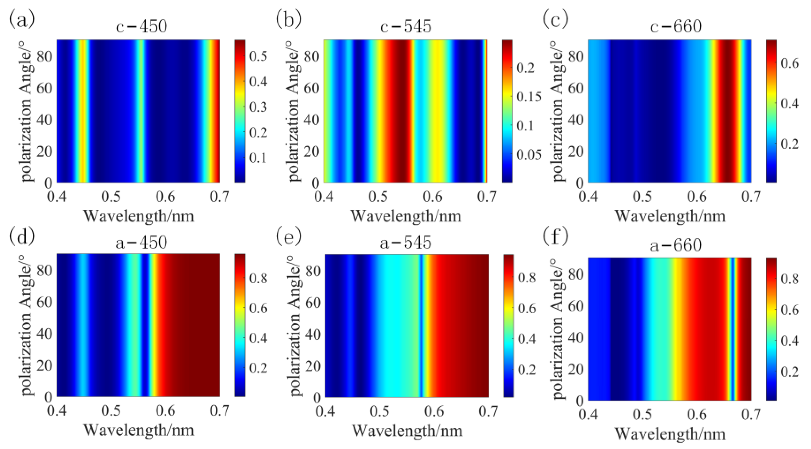
3. Results and Discussion

| Refs. | [17] | [46] | [50] | [52] | This Work |
|---|---|---|---|---|---|
| Material | GST/SiO2/Ag | Si/SiO2 | ITO/GeTe/Al | TiO2/dimers/SiO2 | Sb2S3/SiO2/Ag |
| Structure | Irregular Grating + Multilayer film | Nanoantenna + SiO2 film | Nanoantenna + Multilayer film | Two kinds of anisotropic dielectric nanostructures + SiO2 film | Nanoantenna + Multilayer film |
| Working Bandwidth (nm) | 400–700 nm | 380–780 nm | 400–700 nm | 400–800 nm | 400–700 nm |
| Design Method | Genetic algorithm inverse design optimization | Machine learning inverse design optimization | Forward design optimization | Neural network and evolutionary strategy inverse design optimization | Genetic algorithm inverse design optimization |
| Physical Mechanism | Mie resonance | Mie resonance | MIM resonance | — | Mie resonance |
| Peak Shift Amplitude (R/G/B) | 270/180/230 nm | — | 13/18/10 nm (measure) | — | 250/155/40 nm |
| Chromatic Aberration | 35.42/13.77/23.39 | — | 24.8/24.9/4 | — | 44.1/28.1/64.8 |
| crystallized color gamut (sRGB color space) | 36.4% | — | 6.2% | — | 27.8% |
4. Conclusions
Author Contributions
Funding
Data Availability Statement
Acknowledgments
Conflicts of Interest
References
- Hu, Q.; Lin, K.-T.; Lin, H.; Zhang, Y.; Jia, B. Graphene metapixels for dynamically switchable structural color. ACS Nano 2021, 15, 8930–8939. [Google Scholar] [CrossRef]
- Wen, K.; Zhang, Z.; Jiang, X.; He, J.; Yang, J. Image representation of structure color based on edge detection algorithm. Results Phys. 2020, 19, 103441. [Google Scholar] [CrossRef]
- Yu, Y.; Wen, L.; Song, S.; Chen, Q. Transmissive/reflective structural color filters: Theory and applications. J. Nanomater. 2014, 2014, 6. [Google Scholar] [CrossRef]
- He, Q.; Sun, S.; Xiao, S.; Zhou, L. High-efficiency metasurfaces: Principles, realizations, and applications. Adv. Opt. Mater. 2018, 6, 1800415. [Google Scholar] [CrossRef]
- Zeng, L.; Yang, Y.; Xiao, G. An All-Dielectric Color Filter, with a Wider Color Gamut. Photonics 2022, 9, 680. [Google Scholar] [CrossRef]
- Li, H.; Zhang, X.; Zhou, F.; Xiao, X.; Xu, Y.; Zhang, Z. Tunable color gamut based a symmetric microcavity governed by Sb2S3. Opt. Commun. 2022, 508, 127683. [Google Scholar] [CrossRef]
- Huang, X.; Huang, J.; Yang, L.; Zhang, Z.; Ma, H.; Qian, Y.; Li, C.; Zhang, Z.; Yang, J. All-Dielectric metasurfaces color filter arrays designed by evolutionary search. IEEE Photonics J. 2021, 13, 1–9. [Google Scholar] [CrossRef]
- Park, C.-S.; Koirala, I.; Gao, S.; Shrestha, V.R.; Lee, S.-S.; Choi, D.-Y. Structural color filters based on an all-dielectric metasurface exploiting silicon-rich silicon nitride nanodisks. Opt. Express 2019, 27, 667–679. [Google Scholar] [CrossRef] [PubMed]
- Wen, K.; Jiang, X.; He, J.; Li, G.; Yang, J. Color-adjustable devices based on the surface plasmons effect. Appl. Sci. 2020, 10, 1960. [Google Scholar] [CrossRef]
- Chen, Q.Y.; Liu, F.R.; Zhang, Y.Z.; Zhang, L.L.; Lian, Y.B.; Yin, B.S.; Ma, Q.L.; Rao, K. Enhancing the adjustable range of saturation in color reflectors using a phase-change material as an effective absorption base. J. Phys. D Appl. Phys. 2022, 55, 375105. [Google Scholar] [CrossRef]
- Chen, Y.; Li, Y.; Tang, W.; Tang, Y.; Hu, Y.; Hu, Z.; Deng, J.; Cheah, K.; Li, G. Centimeter scale color printing with grayscale lithography. Adv. Photonics Nexus 2022, 1, 026002. [Google Scholar] [CrossRef]
- Wang, D.; Liu, Z.; Wang, H.; Li, M.; Guo, L.J.; Zhang, C. Structural color generation: From layered thin films to optical metasurfaces. Nanophotonics 2023, 12, 1019–1081. [Google Scholar] [CrossRef]
- Li, H.; Xu, Y.; Zhang, X.; Xiao, X.; Zhou, F.; Zhang, Z. All-dielectric high saturation structural colors enhanced by multipolar modulated metasurfaces. Optics Express 2022, 30, 28954–28965. [Google Scholar] [CrossRef]
- Visser, D.; Basuvalingam, S.B.; Desieres, Y.; Anand, S. Optical properties and fabrication of dielectric metasurfaces based on amorphous silicon nanodisk arrays. Optics Express 2019, 27, 5353–5367. [Google Scholar] [CrossRef] [PubMed]
- Lu, L.; Dong, Z.; Tijiptoharsono, F.; Ng, R.J.H.; Wang, H.; Rezaei, S.D.; Wang, Y.; Leong, H.S.; Lim, P.C.; Yang, J.K. Reversible tuning of Mie resonances in the visible spectrum. ACS Nano 2021, 15, 19722–19732. [Google Scholar] [CrossRef]
- Yang, W.; Qu, G.; Lai, F.; Liu, Y.; Ji, Z.; Xu, Y.; Song, Q.; Han, J.; Xiao, S. Dynamic bifunctional metasurfaces for holography and color display. Adv. Mater. 2021, 33, 2101258. [Google Scholar] [CrossRef] [PubMed]
- Huang, X.; Huang, J.; Qian, Y.; Yang, L.; Zhang, Z.; Yang, J. Nonvolatile phase-change materials color display designed by evolutionary search. Results Phys. 2021, 29, 104701. [Google Scholar] [CrossRef]
- Zhao, J.; Zhou, Y.; Huo, Y.; Gao, B.; Ma, Y.; Yu, Y. Flexible dynamic structural color based on an ultrathin asymmetric Fabry-Perot cavity with phase-change material for temperature perception. Optics Express 2021, 29, 23273–23281. [Google Scholar] [CrossRef]
- Kim, J.; Park, C.; Hahn, J.W. Metal–Semiconductor–Metal Metasurface for Multiband Infrared Stealth Technology Using Camouflage Color Pattern in Visible Range. Adv. Opt. Mater. 2022, 10, 2101930. [Google Scholar] [CrossRef]
- Jia, W.; Menon, R.; Sensale-Rodriguez, B. Reconfigurable and programmable optical devices with phase change materials Sb2S3 and Sb2Se3. In Proceedings of the Active Photonic Platforms 2022, San Diego, CA, USA, 3 October 2022; pp. 12–18. [Google Scholar]
- Koirala, I.; Lee, S.-S.; Choi, D.-Y. Highly transmissive subtractive color filters based on an all-dielectric metasurface incorporating TiO2 nanopillars. Optics Express 2018, 26, 18320–18330. [Google Scholar] [CrossRef]
- Berzins, J.; Silvestri, F.; Gerini, G.; Setzpfandt, F.; Pertsch, T.; Bäumer, S.M. Color filter arrays based on dielectric metasurface elements. In Proceedings of the Metamaterials XI, Strasbourg, France, 14 May 2018; pp. 89–99. [Google Scholar]
- Xuan, Z.; Li, J.; Liu, Q.; Yi, F.; Wang, S.; Lu, W. Artificial structural colors and applications. Innovation 2021, 2, 100081. [Google Scholar] [CrossRef]
- de Galarreta, C.R.; Sinev, I.; Alexeev, A.M.; Trofimov, P.; Ladutenko, K.; Carrillo, S.G.-C.; Gemo, E.; Baldycheva, A.; Bertolotti, J.; Wright, C.D. Reconfigurable multilevel control of hybrid all-dielectric phase-change metasurfaces. Optica 2020, 7, 476–484. [Google Scholar] [CrossRef]
- Wang, L.; Wang, T.; Yan, R.; Yue, X.; Wang, H.; Wang, Y.; Zhang, J. Tunable structural colors generated by hybrid Si3N4 and Al metasurfaces. Optics Express 2022, 30, 7299–7307. [Google Scholar] [CrossRef]
- Wuttig, M.; Bhaskaran, H.; Taubner, T. Phase-change materials for non-volatile photonic applications. Nat. Photonics 2017, 11, 465–476. [Google Scholar] [CrossRef]
- Wang, Q.; Rogers, E.T.; Gholipour, B.; Wang, C.-M.; Yuan, G.; Teng, J.; Zheludev, N.I. Optically reconfigurable metasurfaces and photonic devices based on phase change materials. Nat. Photonics 2016, 10, 60–65. [Google Scholar] [CrossRef]
- Shportko, K.; Kremers, S.; Woda, M.; Lencer, D.; Robertson, J.; Wuttig, M. Resonant bonding in crystalline phase-change materials. Nat. Mater. 2008, 7, 653–658. [Google Scholar] [CrossRef] [PubMed]
- Li, X.; Luo, M.; Jiang, X.; Luo, S.; Yang, J. Tunable Color-Variable Solar Absorber Based on Phase Change Material Sb2Se3. Nanomaterials 2022, 12, 1903. [Google Scholar] [CrossRef]
- Zhao, K.; Han, W.; Han, Z.; Zhang, X.; Zhang, X.; Duan, X.; Wang, M.; Yuan, Y.; Zuo, P. Ultrafast laser-induced integrated property–structure modulation of Ge2Sb2Te5 for multifunction and multilevel rewritable optical recording. Nanophotonics 2022, 11, 3101–3113. [Google Scholar] [CrossRef]
- Delaney, M.; Zeimpekis, I.; Lawson, D.; Hewak, D.W.; Muskens, O.L. A new family of ultralow loss reversible phase-change materials for photonic integrated circuits: Sb2S3 and Sb2Se3. Adv. Funct. Mater. 2020, 30, 2002447. [Google Scholar] [CrossRef]
- Jia, W.; Menon, R.; Sensale-Rodriguez, B. Visible and near-infrared programmable multi-level diffractive lenses with phase change material Sb2S3. Optics Express 2022, 30, 6808–6817. [Google Scholar] [CrossRef]
- Sahoo, D.; Naik, R. GSST phase change materials and its utilization in optoelectronic devices: A review. Mater. Res. Bull. 2022, 148, 111679. [Google Scholar] [CrossRef]
- Ni, Z.; Mou, S.; Zhou, T.; Cheng, Z. Broader color gamut of color-modulating optical coating display based on indium tin oxide and phase change materials. Appl. Opt. 2018, 57, 3385–3389. [Google Scholar] [CrossRef]
- Dong, W.; Liu, H.; Behera, J.K.; Lu, L.; Ng, R.J.; Sreekanth, K.V.; Zhou, X.; Yang, J.K.; Simpson, R.E. Wide bandgap phase change material tuned visible photonics. Adv. Funct. Mater. 2019, 29, 1806181. [Google Scholar] [CrossRef]
- Fang, Z.; Zheng, J.; Saxena, A.; Whitehead, J.; Chen, Y.; Majumdar, A. Non-volatile reconfigurable integrated photonics enabled by broadband low-loss phase change material. Adv. Opt. Mater. 2021, 9, 2002049. [Google Scholar] [CrossRef]
- Kriisa, M.; Krunks, M.; Acik, I.O.; Kärber, E.; Mikli, V. The effect of tartaric acid in the deposition of Sb2S3 films by chemical spray pyrolysis. Mater. Sci. Semicond. Process. 2015, 40, 867–872. [Google Scholar] [CrossRef]
- Hong, J.-Y.; Lin, L.-Y.; Li, X. Electrodeposition of Sb2S3 light absorbers on TiO2 nanorod array as photocatalyst for water oxidation. Thin Solid Films 2018, 651, 124–130. [Google Scholar] [CrossRef]
- Li, S.a.; Zhang, Y.; Tang, R.; Wang, X.; Zhang, T.; Jiang, G.; Liu, W.; Zhu, C.; Chen, T. Aqueous-Solution-Based Approach Towards Carbon-Free Sb2S3 Films for High Efficiency Solar Cells. ChemSusChem 2018, 11, 3208–3214. [Google Scholar] [CrossRef] [PubMed]
- Mane, R.; Lokhande, C. Thickness-dependent properties of chemically deposited Sb2S3 thin films. Mater. Chem. Phys. 2003, 82, 347–354. [Google Scholar] [CrossRef]
- Arun, P.; Vedeshwar, A. Effect of heat treatment on the optical properties of amorphous Sb2S3 film: The possibility of optical storage. J. Non Cryst. Solids 1997, 220, 63–68. [Google Scholar] [CrossRef]
- El-Shazly, A.; Seyam, M.; El-Samanoudy, M.; Ammar, A.; Assim, E. The effect of deposition rate and heat treatment on conduction and charge carrier transport mechanisms in Sb2S3 films. Appl. Surf. Sci. 2002, 189, 129–137. [Google Scholar] [CrossRef]
- Arun, P.; Vedeshwar, A.; Mehra, N. Laser-induced crystallization in amorphous films of (C= S, Se, Te), potential optical storage media. J. Phys. D Appl. Phys. 1999, 32, 183. [Google Scholar] [CrossRef]
- Gao, K.; Du, K.; Tian, S.; Wang, H.; Zhang, L.; Guo, Y.; Luo, B.; Zhang, W.; Mei, T. Intermediate Phase-Change States with Improved Cycling Durability of Sb2S3 by Femtosecond Multi-Pulse Laser Irradiation. Adv. Funct. Mater. 2021, 31, 2103327. [Google Scholar] [CrossRef]
- Panda, S.S.; Hegde, R.S. Transmission-mode all-dielectric metasurface color filter arrays designed by evolutionary search. J. Nanophotonics 2020, 14, 016014. [Google Scholar] [CrossRef]
- Huang, Z.; Liu, X.; Zang, J. The inverse design of structural color using machine learning. Nanoscale 2019, 11, 21748–21758. [Google Scholar] [CrossRef]
- Dai, P.; Sun, K.; Muskens, O.L.; De Groot, C.; Huang, R. Inverse design of a vanadium dioxide based dynamic structural color via conditional generative adversarial networks. Opt. Mater. Express 2022, 12, 3970–3981. [Google Scholar] [CrossRef]
- Jiang, X.; Yuan, H.; Chen, D.; Zhang, Z.; Du, T.; Ma, H.; Yang, J. Metasurface based on inverse design for maximizing solar spectral absorption. Adv. Opt. Mater. 2021, 9, 2100575. [Google Scholar] [CrossRef]
- Sharma, G.; Wu, W.; Dalal, E.N. The CIEDE2000 color-difference formula: Implementation notes, supplementary test data, and mathematical observations. Color Res. Appl. 2005, 30, 21–30. [Google Scholar] [CrossRef]
- Carrillo, S.G.C.; Trimby, L.; Au, Y.Y.; Nagareddy, V.K.; Rodriguez-Hernandez, G.; Hosseini, P.; Ríos, C.; Bhaskaran, H.; Wright, C.D. A nonvolatile phase-change metamaterial color display. Adv. Opt. Mater. 2019, 7, 1801782. [Google Scholar] [CrossRef]
- Zeng, Q.; Duan, S.; Zhao, Z.; Wang, P.; Lei, H. Inverse Design of Energy-Absorbing Metamaterials by Topology Optimization. Adv. Sci. 2023, 10, 2204977. [Google Scholar] [CrossRef]
- Ma, D.; Li, Z.; Liu, W.; Geng, G.; Cheng, H.; Li, J.; Tian, J.; Chen, S. Deep-learning enabled multicolor meta-holography. Adv. Opt. Mater. 2022, 10, 2102628. [Google Scholar] [CrossRef]
- Hosseini, P.; Wright, C.D.; Bhaskaran, H. An optoelectronic framework enabled by low-dimensional phase-change films. Nature 2014, 511, 206–211. [Google Scholar] [CrossRef] [PubMed]
- Virt, I.; Rudyj, I.; Kurilo, I.; Lopatynskyi, I.Y.; Linnik, L.; Tetyorkin, V.; Potera, P.; Luka, G. Properties of Sb2S3 and Sb2Se3 thin films obtained by pulsed laser ablation. Semiconductors 2013, 47, 1003–1007. [Google Scholar] [CrossRef]


| PCM | Conversion Temperature | Melting Point | Bandgap | Switching Time | Phase Change Cyclicity | ∆n at 633 nm | kc at 633 nm | ∆n/kc at 633 nm |
|---|---|---|---|---|---|---|---|---|
| /K | /K | /eV | /s | /Frequency | ||||
| GSST [33] | 673 | 900 | — | — | 105 | 0.16 | 3.82 | 0.04 |
| GST [34,35] | 453 | 889 | 0.4~0.7 | 50 × 10−9 | 1015 | 0.62 | 2.56 | 0.24 |
| Sb2S3 [15,32,36,37,38,39,40,41,42,43,44] | 573 | 823 | 1.7~2 | 80 × 10−9 | >7000 | 0.87 | 0.56 | 1.55 |
| Target Wavelength | Height of Circle | Outer Diameter of Circle | Inner Diameter of Circle | Substrate Period |
|---|---|---|---|---|
| /nm | H/nm | R/nm | r/nm | P/nm |
| 450 | 119 | 84 | 0 | 366 |
| 545 | 84 | 127 | 0 | 372 |
| 660 | 111 | 130 | 63 | 440 |
Disclaimer/Publisher’s Note: The statements, opinions and data contained in all publications are solely those of the individual author(s) and contributor(s) and not of MDPI and/or the editor(s). MDPI and/or the editor(s) disclaim responsibility for any injury to people or property resulting from any ideas, methods, instructions or products referred to in the content. |
© 2023 by the authors. Licensee MDPI, Basel, Switzerland. This article is an open access article distributed under the terms and conditions of the Creative Commons Attribution (CC BY) license (https://creativecommons.org/licenses/by/4.0/).
Share and Cite
Wei, X.; Nong, J.; Zhang, Y.; Ma, H.; Huang, R.; Yuan, Z.; Zhang, Z.; Zhang, Z.; Yang, J. Sb2S3-Based Dynamically Tuned Color Filter Array via Genetic Algorithm. Nanomaterials 2023, 13, 1452. https://doi.org/10.3390/nano13091452
Wei X, Nong J, Zhang Y, Ma H, Huang R, Yuan Z, Zhang Z, Zhang Z, Yang J. Sb2S3-Based Dynamically Tuned Color Filter Array via Genetic Algorithm. Nanomaterials. 2023; 13(9):1452. https://doi.org/10.3390/nano13091452
Chicago/Turabian StyleWei, Xueling, Jie Nong, Yiyi Zhang, Hansi Ma, Rixing Huang, Zhenkun Yuan, Zhenfu Zhang, Zhenrong Zhang, and Junbo Yang. 2023. "Sb2S3-Based Dynamically Tuned Color Filter Array via Genetic Algorithm" Nanomaterials 13, no. 9: 1452. https://doi.org/10.3390/nano13091452