Article

Lead-Free Perovskite Thin Films for Gas Sensing through Surface Acoustic Wave Device Detection

by
Nicoleta Enea
1,2,3,
Valentin Ion
1,*,
Cristian Viespe
1,
Izabela Constantinoiu
1,
Anca Bonciu
1,
Maria Luiza Stîngescu
1,3,
Ruxandra Bîrjega
1 and
Nicu Doinel Scarisoreanu
1
1
National Institute for Laser, Plasma and Radiation Physics, 077125 Magurele, Romania
2
Department of Physics and Astronomy, University of Florence, Via G. Sansone 1, 50019 Sesto Fiorentino, FI, Italy
3
Faculty of Physics, University of Bucharest, 077125 Magurele, Romania
*
Author to whom correspondence should be addressed.
Nanomaterials 2024, 14(1), 39; https://doi.org/10.3390/nano14010039
Submission received: 29 November 2023 / Revised: 18 December 2023 / Accepted: 20 December 2023 / Published: 22 December 2023
(This article belongs to the Special Issue New Challenges in Designed Nanointerfaces)

Abstract

:
Thin film technology shows great promise in fabricating electronic devices such as gas sensors. Here, we report the fabrication of surface acoustic wave (SAW) sensors based on thin films of (1 − x) Ba(Ti0.8Zr0.2)O3−x(Ba0.7Ca0.3)TiO3 (BCTZ50, x = 50) and Polyethylenimine (PEI). The layers were deposited by two laser-based techniques, namely pulsed laser deposition (PLD) for the lead-free material and matrix assisted pulsed laser evaporation (MAPLE) for the sensitive polymer. In order to assay the impact of the thickness, the number of laser pulses was varied, leading to thicknesses between 50 and 350 nm. The influence of BCTZ film’s crystallographic features on the characteristics and performance of the SAW device was studied by employing substrates with different crystal structures, more precisely cubic Strontium Titanate (SrTiO3) and orthorhombic Gadolinium Scandium Oxide (GdScO3). The SAW sensors were further integrated into a testing system to evaluate the response of the BCTZ thin films with PEI, and then subjected to tests for N2, CO2 and O2 gases. The influence of the MAPLE’s deposited PEI layer on the overall performance was demonstrated. For the SAW sensors based on BCTZ/GdScO3 thin films with a PEI polymer, a maximum frequency shift of 39.5 kHz has been obtained for CO2; eight times higher compared to the sensor without the polymeric layer.

1. Introduction

In an era where the demand for air quality monitoring to ensure the safety of the environment and human health has increased, gas sensors have become crucial for the detection of various gases (such as volatile organic compounds [1], inorganic gases [2,3,4,5,6,7,8,9,10], etc.). In the last few decades, surface acoustic wave (SAW) technology has been integrated into gas detection devices, providing them with attractive advantages such as compactness, portability, low-cost manufacturing, high sensitivity and accuracy, real-time measurements and good reliability [11,12,13]. Moreover, through a suitable choice of materials for fabricating these types of sensors, they also offer outstanding characteristics like selectivity, reversibility and linearity [14]. An SAW gas sensor (Rayleigh-wave, delay-line type sensor) consists of an expensive piezoelectric single-crystal material (usually ST-Quartz or LiNbO3) with interdigital transducer electrodes (IDTs) deposited on its surface and a recognition layer in-between.
SAW devices convert the input electrical signal sent through IDT into a mechanical one, which is subsequently altered by the sensing event and converted back into an electrical one through the output IDT. The changes produced by the exposure of the detection layer to the target analyte consist of variations in the amplitude, frequency and phase of the output signal relative to the input signal [15,16,17].
Regarding the sensing layers, a wide range of materials have been exploited for these SAW devices [11,18,19]. Common materials such as conductive/non-conductive polymers and metal oxides have been chosen most often to recognise gas molecules [20,21]. But other materials have also been tested, including carbon-based nanostructures [22,23,24,25], composite materials [26,27], metals [28], metal-organic frameworks [29] and porous materials [30]. There are some reports in the literature on using a ferroelectric lead zirconium titanate (PZT) thin film as the sensing layer to improve the coupling coefficient of SAW devices [3,31,32]. In addition, a low-cost SAW device based on a thin layer of PZT deposited on a non-piezoelectric substrate was reported [33], but detailed studies on the use of thin films of lead-free ferroelectric materials for gas sensing in SAW devices are scarce. Multi-component systems of lead titanate (PbTiO3) and lead zirconate (PbZrO3), called lead zirconium titanate (Pb[ZrxTi1−x]O3 (0 ≤ x ≤ 1)—PZT), are the most widely employed perovskite ceramic materials due to their advantageous properties, such as greater sensitivity and higher operating temperature, compared to other piezo ceramics [34,35]. Since 2006, legislation restricts the use of materials that pose risks to human health and to the environment, thus lead-based materials are considered to be particularly toxic and, in this regard, the attention of researchers has turned to other lead-free piezoelectric materials.
Among this class of eco-friendly materials, barium titanate (BaTiO3-BT) was the first ceramic material with ferroelectric properties ever discovered, but the interest in it declined after the discovery of PZT, whose piezoelectric properties were superior [36]. The potential of using BT-based ceramics in piezoelectric applications was reconsidered after 2009, when Liu and Ren found a surprisingly high piezoelectric coefficient (d33∼620  pC/N) for the non-lead ceramic system Ba(Ti0.8Zr0.2)O3−(Ba0.7Ca0.3)TiO3 [37]. This strategy for improving the piezoelectric response of BT by introducing Ca2+ and Zr4+ into its crystal structure has led to increased research papers on this topic [38]. Lead-free piezoelectric materials (Ba, Ca)(Ti, Zr)O3 (BCTZ) with different properties were obtained by varying the concentrations of the two ferroelectric oxides Ba(Ti0.8Zr0.2)O3 and (Ba0.7Ca0.3)TiO3, which enables their use in applications such as energy harvesting and storage or actuators. Different techniques for growing thin layers of BCTZ on various substrates have been reported in the literature, from chemical ones, like the sol-gel method [39], to physical ones, namely, RF magnetron sputtering [40] and pulsed laser deposition [41].
Using polymer-inorganic composites was demonstrated to result in high-performance gas sensors due to the synergistic effects [42] between specific functional materials when used with an adequate fabrication technology. Numerous polymers can be used as sensing materials, for instance, polypyrrole (PPy), polyaniline (Pani) or polythiophene and their derivatives [43,44]. In this present work, we selected polyethylenimine (PEI) to obtain hybrid layers of polymer-inorganic composites.
Motivated by the possibility of using lead-free piezoelectric/ferroelectric materials for SAW devices [3], [33], here we report the fabrication and functional properties of surface acoustic wave (SAW) sensors based on thin films of (1 − x) Ba(Ti0.8Zr0.2)O3−x(Ba0.7Ca0.3)TiO3 (BCTZ50) in combination with a Polyethylenimine (PEI) layer, using laser-based deposition techniques to obtain both inorganic and organic layers. As the various characteristics of an active sensor element (i.e., thickness, crystalline structure, surface roughness, chemistry, etc) can influence the response of an SAW sensor to a specific analyte, the thin layers of BCTZ50 were deposited by pulsed laser deposition (PLD) onto different monocrystalline substrates (SrTiO3, GdScO3) to induce different epitaxial characteristics (strain, texture) into the film’s crystalline structure. This was followed by depositing a PEI polymer on top of the epiatxial BCTZ50 thin films using the matrix assisted pulsed laser evaporation (MAPLE) technique. The structures obtained were further integrated into SAW devices to evaluate their sensing properties in different gaseous environment.

2. Materials and Methods

2.1. Deposition of Thin Films

The (1 − x) Ba(Ti0.8Zr0.2)O3−x(Ba0.7Ca0.3)TiO3 (BCTZx) thin films were deposited by pulsed laser deposition (PLD) using the x = 50 composition.
BCTZ50 targets were prepared via the conventional sintering route, starting from precursors and followed by milling, pressing and sintering at high temperature (1450 °C).
The substrates used for deposition were monocrystalline Strontium Titanate (SrTiO3 or STO) and Gadolinium Scandium Oxide (GdScO3 or GSO). For the fabrication of the BCTZ50/STO and BCTZ50/GSO samples, an ArF excimer laser was used, the laser fluence value being 1.65 J/cm2. The number of laser pulses ranged between 8000 and 36,000, with a 5 Hz repetition rate. The substrate temperature was set to 700 °C, with a heating rate of 50 °C/min while the cooling rate was set to 10 °C/min. The flow of oxygen during the ablation process was set to 20 sccm and the gas pressure reached 1 × 10⁻¹ mbar, before starting laser ablation. When the ablation process ended, the cooling of the substrates was performed in oxygen flow, set to 200 sccm.
The Polyethylenimine (PEI) polymer was deposited using matrix assisted pulsed laser evaporation (MAPLE). The MAPLE deposition method involves obtaining a target from a polymer dissolved in a solvent (matrix). The PEI target was obtained by dissolving 400 mg of PEI in a 1:1 solution of deionised water and isopropyl alcohol, under magnetic stirring, for 60 min. The target thus obtained was frozen in liquid nitrogen and further irradiated, using 266 nm of a Nd:YAG laser, at 10 Hz with 36,000 laser pulses.
The surface acoustic wave sensors (SAW) were used to evaluate the response of BCTZ thin film covered and uncovered with PEI. For the gas response measurement, interdigital electrodes were deposited on the surface of thin films via thermal evaporation.
For the IDT, Au metal electrodes were deposited, with thicknesses of approximately 200 nm on the BCTZ thin layers. Later, gold wires with a diameter of 75 µm were glued to the electrodes, using an epoxy conductive silver (Ag). The sensors were tested and characterised for different types of usual gases (O2, CO2 and N2), at room temperature and with a humidity of 60%. The humidity was monitored using a hygrometer.
Using the methods and techniques described above, an evaluation of the gas response of BCTZ50 and PEI/BCTZ50 structure was conducted.

2.2. Thin Layer Characterization

In this study, we explored the surface morphology of the samples through scanning electron microscopy (SEM). Our analyses were performed using the Scios 2 DualBeam, an advanced ultra-high-resolution analytically focused ion beam scanning electron microscopy FIB-SEM system (Thermo Fisher Scientific Inc. in Hillsboro, OR, USA), at voltages reaching up to 30 kV. The topography of the probes was further analysed by employing atomic force microscopy (AFM) (XE 100 AFM, Park systems KANC 15F, Gwanggyo-ro, Suwon, Republic of Korea) and the measurements were performed in non-contact mode.
Optical properties were investigated by spectroscopic ellipsometry measurements on a Woollam Variable Angle Spectroscopic Ellipsometer (VASE) system equipped with a high-pressure Xe discharge lamp. The spectral range analysed was 1–5 eV, representing the near IR to the UV (260–1200 nm) spectrum and was carried out at a fixed angle of incidence. For obtaining the refractive indexes and extinction coefficients of the analysed layers, WVASE32 software (VASE, J.A. Woollam Co., Inc., Lincoln, NE, USA) was used for fitting and extracting the data from complex multilayer response.
High-resolution X-ray diffraction was conducted on a PANalytical X’pert MRD system (Almelo, The Netherlands) using a parallel monochromatic beam of CuKα1 (λ = 1.540598 Å) provided by a four-bonce crystal of Ge(220) placed in the incident beam.

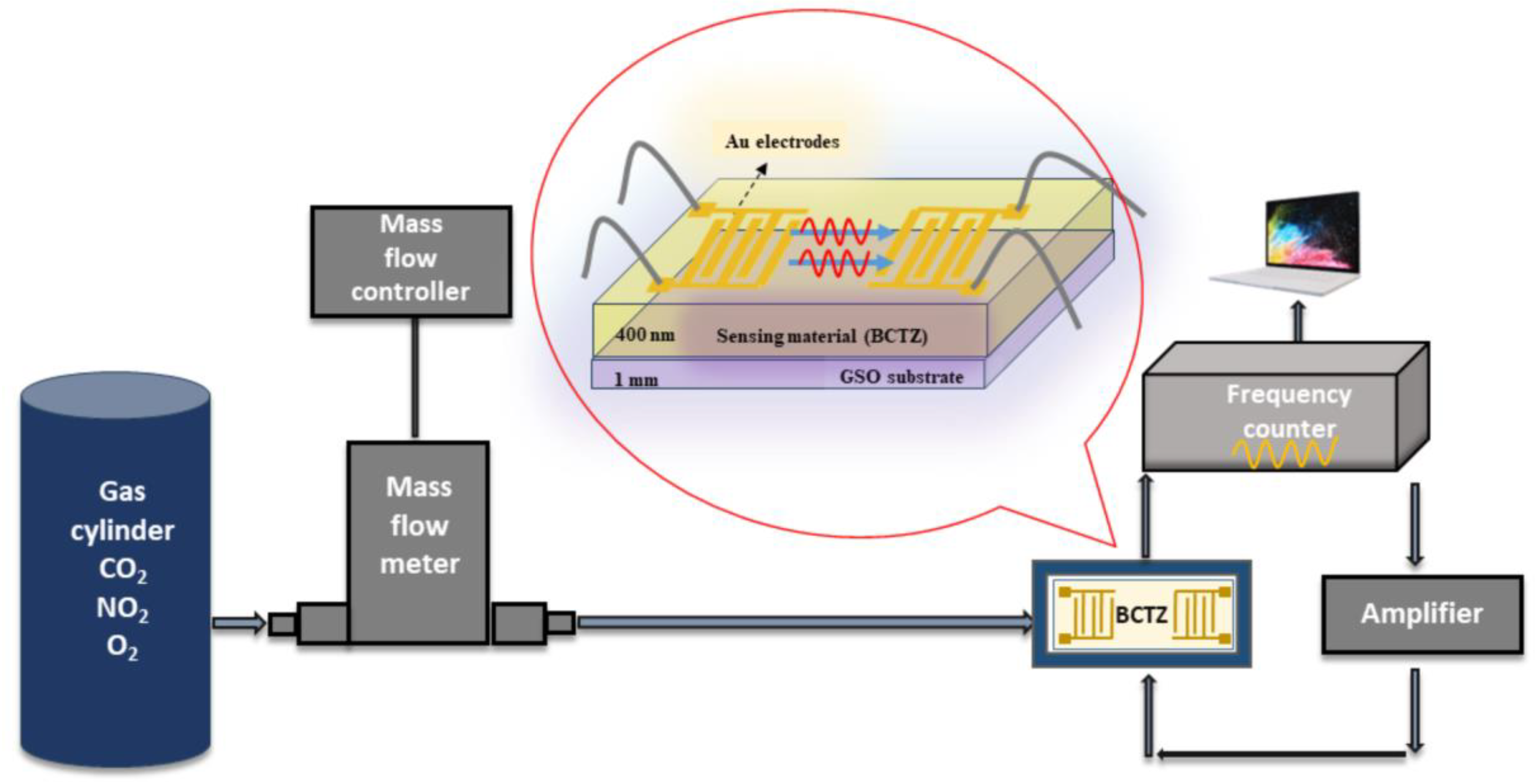
2.3. SAW Measurements

The SAW testing system was composed of an amplifier (DHPVA-200 FEMTO amplifier—Messtechnik GmbH, Berlin, Germany), a frequency counter (CNT-91 Pendulum—Spectracom Corp, Rochester, NY, USA) connected to a computer with specialised software. The gas flow was ensured by a mass flow controller, through a mass flow meter, and the gas concentration used for testing was: N2—99.996%; CO2—99.998%; and O2—99.999%; with a gas flow of 0.5 L/min. All investigations were performed at room temperature.

3. Results and Discussion

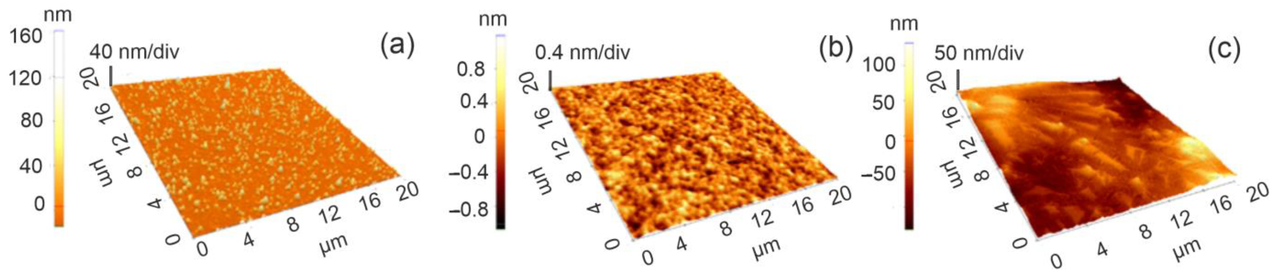
3.1. AFM and SEM Morphological Characterization

Scanning electron microscopy and atomic force microscopy were used first to analyse the morphology and roughness of the deposited coatings surfaces. Examples of the SEM images with a magnification of 20 k of the samples obtained by PLD are presented in Figure 1.
The SEM analysis provided valuable insights into the characteristics of thin films deposited using Pulsed Laser Deposition (PLD) on different substrates. Specifically, when applied to Strontium Titanate (STO) substrates, PLD consistently yielded thin films with a uniform distribution across the surface. However, a notable observation was the regular accumulation of material in the form of grains on the surface; a phenomenon commonly associated with PLD technique.
Despite the presence of these surface grains, an interesting finding emerged: the overall appearance and characteristics of the film surfaces did not undergo significant changes even when the number of pulses was varied. This suggests a robustness in the PLD-deposited films on STO substrates, as their fundamental properties appeared to remain stable under different deposition conditions.
In contrast to the STO substrates, the examination of Barium Calcium Titanate Zirconate (BCTZ) films on Gadolinium Scandium Oxide (GSO) revealed a distinctly different outcome. The SEM analysis highlighted the remarkably smooth surface morphology for the BCTZ film on GSO. This indicates that the interaction between the PLD technique and the GSO substrate resulted in a unique deposition behaviour, leading to a more even and homogeneous film surface.
These observations not only contribute to our understanding of the PLD process, but also underscore the significance of substrate selection in determining the final morphology of thin films. The ability to control and manipulate the surface characteristics of deposited films is crucial for various applications.
For a better visualization of the surface topography, and to understand the material organization on the surfaces, AFM measurements were performed.
The influence of the substrate can easily be seen through the appearance of columnar grains of maximum 40 nm, in the case of the thin film deposited on GdScO3, compared with the one on SrTiO3, where the surface morphology became smoother. In all cases, the surface was uniformly covered by the deposited thin films, with no defects, and the roughness of the layers was found to be between 4 and 40 nm.
In contrast with the BCTZ samples, the main characteristic for the PEI/BCTZ layered coatings, as confirmed by both SEM and AFM analysis, is a low roughness on the surface, as can be seen in Figure 1b and Figure 2c. MAPLE-deposited PEI layers were smooth, with no cracks, and the two employed analysis techniques revealed uniformly distributed films, covering the entire surface of the probes, in accordance with other studies published in the literature [45].

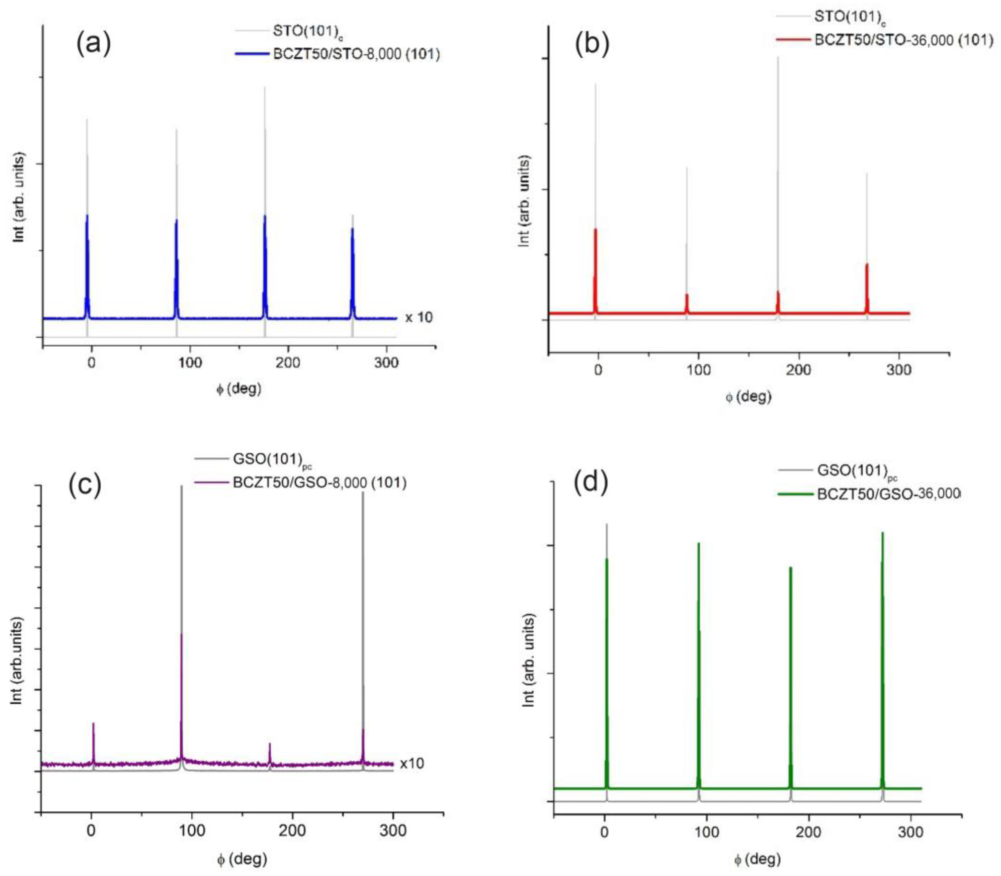
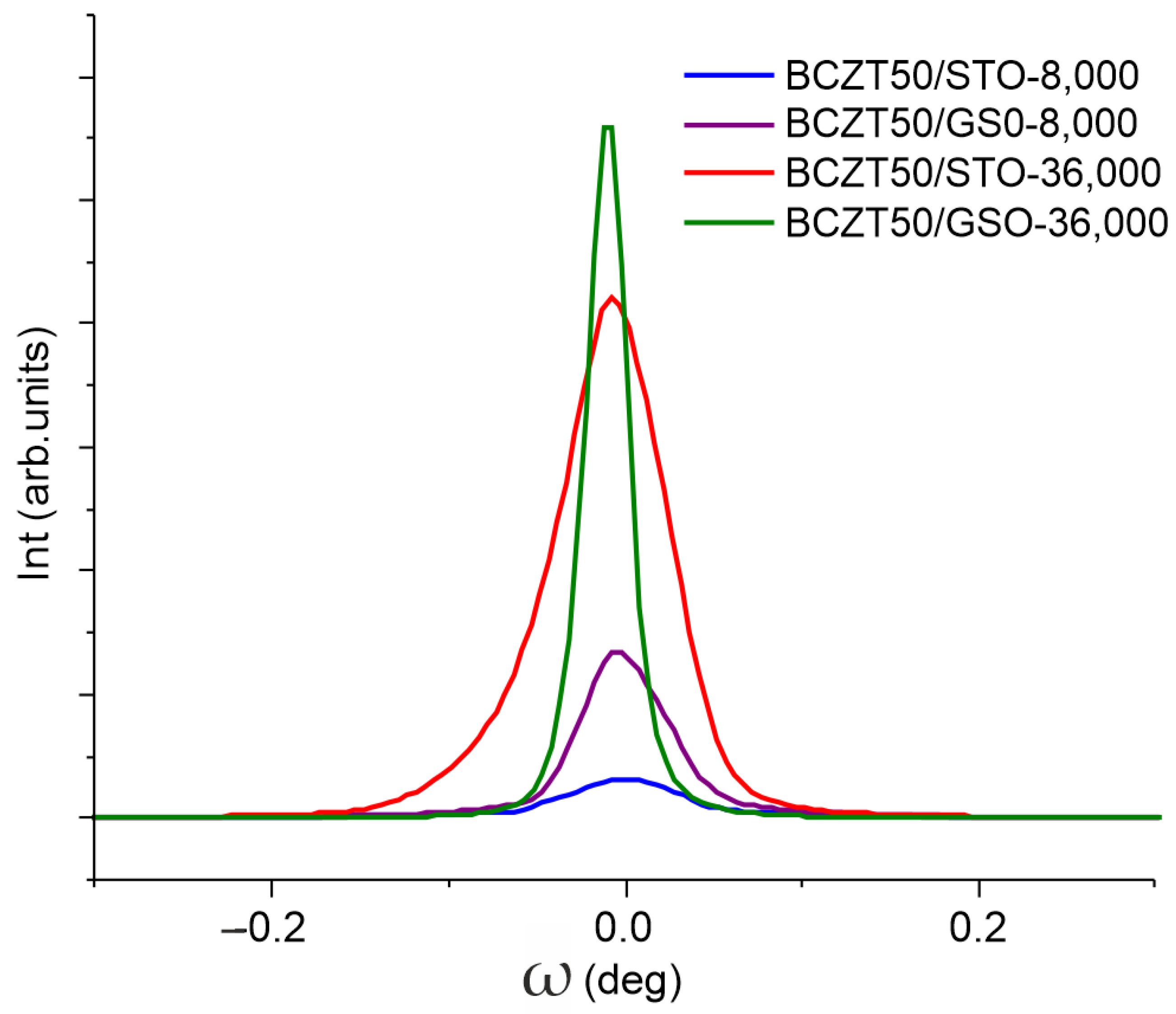
3.2. XRD Measurements

The films were deposited on (001)-oriented cubic STO substrates and (110)-oriented orthorhombic GSO substrates, respectively. For simplicity, and for comparison, we considered a pseudocubic lattice for GSO. The orthorhombic (110) orientation of GSO is equivalent to the (001) of a pseudocubic symmetry, and consequently, the substrates were prescribed the subscript “pc” for GSO and “c” for STO. STO has a cubic lattice parameter of 3.905 Å, and GSO has a pseudocubic lattice parameter of 3.967 Å [46]. Figure 3 displays the conventional X-ray 2θ-θ scans for the BCZT films on (b) STO and (c) GSO substrates. The x = 50 value for BCZT target is, at room temperature, near the morphotropic phase boundary (MPB) separating the rhombohedral (R) and tetragonal (T) phases by an intermediate orthorhorombic (O) phase. The target BCZT50 XRD patterns exhibits a distorted orthorhombic phase which we had refined in a cubic symmetry (S.G. Pm-3m) to obtain a pseudocubic lattice parameter of 4.0118 Å [47], consistent with the standard BCZT powder XRD pattern, ICDD card no. 00-063-0614 (Figure 3a). All the films show only the (00l) reflections with no secondary phase, revealing a fully epitaxial growth. The epitaxial coherent growth of the BCZT films is confirmed by the four-circle Φ scans around (101) BCZT and their corresponding (101)c STO and (101)pc-GSO reflections, respectively. For all the films, a fourfold symmetry is clearly seen (Figure 4).
The out-of-plane and in-plane lattice parameters were determined from conventional and off-axis scans. The mosaicity of the films is described by the ω-scans of the (00l) symmetric reflections. Figure 5 presents the superimposed ω-scans of the (002) reflections of the BCZT50 films deposited on STO and GSO. From the evolution of the broadening of these ω-scans of the (00l) reflections, using the Williamson–Hall approach proposed by Mentzger et al. [48], the lateral coherence length, which is parallel to the substrate (L), and the mean mosaic tilt angle (αtilt) were extracted. We employed the approach described in our previous works [41,47]. The structural data are gathered in Table 1, along with the values of the degree of the in-plane strain due to the misfit relative to the substrate, εin-plane, calculated as (ain-planeasubstrate)/asubstrate ∗ 100%.
An examination of the structural data collected in Table 1 shows the results to be related to the nature of the substrate (STO or GSO) and to the thickness of the films controlled by the used number of laser pulses. Furthermore, one can see that the smallest in-plane strain values are obtained for the thin films deposited onto GSO, due to GSO’s larger pseudocubic lattice parameter. Apparently, the thickness of the thin films affects their mosaicity: the lateral coherence length increases with the thickness while the mean mosaic tilt angle decreases.
With the improved mosaicity, the crystallinity of the thicker-strained relaxed films is clearly emphasised by the broadness of rocking curves in the BCZT (002) plane, as presented in Figure 5. However, for the thin films deposited onto GSO substrates, one should bear in mind the actual orthorhombic symmetry of the substrate which induces anisotropic strains in the BCZT films, which generates interesting structural features [49].

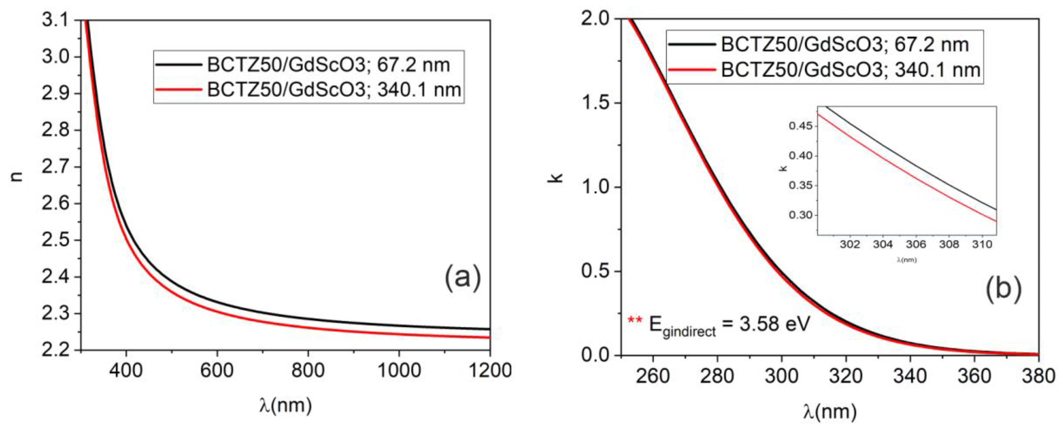
3.3. Optical Properties: Spectrometric Ellipsometry (SE)

Ellipsometry measurements were carried out to evaluate the optical properties of BCTZ samples by performing measurements in the 260–1200 wavelength nm range, at room temperature. The Δ and ψ parameters are the phase difference and amplitude ratio in the electric field; they describe the change in polarization (from circular to elliptic polarization) and were fitted by building an optical model. The change in polarization state occurs when the incident light beam interacts with measured structure. Δ and ψ depend on the optical properties of the analysed structures and the thicknesses of material layers. In this case, the samples were thin layers of BCTZ deposited on monocrystalline substrates (SrTiO3 and GdScO3). The optical model consisted of a stack of three layers: the substrate, the deposited BCTZ layer and the rough top layer. Each layer was characterised by its own dielectric function (optical properties). For the monocrystalline substrates, we performed the SE measurement before the PLD deposition and we calculated the dispersion of “n” and “k” by fitting Δ and ψ and using point-by-point regression analysis [50]. The BCTZ layer was fitted by a single Gauss oscillator and the top rough layer was assumed to consist of 50% air and 50% BCTZ in a Bruggeman approximation.
The calculated thicknesses of the BCTZ layer and the value of roughness are presented in Table 2. In the case of BCTZ50 deposited with 8000 laser pulses, thicknesses values between 60 and 100 nm were obtained, with a roughness of a few nanometres. When the number of laser pulses increased to 36,000, the obtained thickness was more than three times higher. The was no linear relation between laser pulses and the calculated thickness, even if the rest of deposition parameters were kept constant (oxygen pressure, distance between target and substrate, laser fluency and substrate temperature) during the PLD process.
When using 36,000 laser pulses, the thickness increased a few times and there were no significant differences between the values of refractive indexes in the visible-IR spectral zone (Figure 6). Nevertheless, the extinction coefficient values were slightly different. For the 8000 BCTZ sample, “k” was higher (k~0.6 at λ = 300 nm, compared to k~0.4 for 36,000 pulses) and the difference can be explained by the strain induced in the thin film caused by the difference between the SrTiO3 substrate lattice constant (cubic with a = 3.905 Å) and the lattice constant of BCTZ50 (pseudo-cubic with a(pc) = 4.0118 Å). When the sample thickness increased, the thin film relaxed, and the properties were found to be similar with bulk BCTZ. For BTCZ thin film deposited on STO, because there is a difference between the Zr and Ca atom radii, which led to slightly different packing density, we obtained different values of optical constants.
In the case of a BCTZ thin layer grown on GdScO3 monocrystalline substrate, a similar optical behaviour to the BCTZx grown on STO was obtained (Figure 7).
For the band gap calculation, Tauc plotting was employed [46]. By plotting the absorption coefficient α (α = 4πk/λ) as a function of photon energy (eV), the values of the band gap are obtained. BaTiO3 (BTO) in a tetragonal structure presents with an indirect band gap [47], with an energy value of 3.41 eV. Instead of BTO, the value of the indirect band gap for BCTZ50 grown on STO substrate was found be higher, Egindirect = 3.54 eV.
In the case of a BCTZ thin layer grown on a GdScO3 monocrystalline substrate, a similar optical behaviour to the BCTZx grown on STO was obtained. The value of the refractive index at λ = 600 nm for BCTZ50 was n = 2.311, instead of n = 2.332 for BCTZ50/STO. The values of the GSO extinction coefficients were found to be higher for samples grown on STO: a value of k = 0.45 for BCTZ50/GSO and k = 0.7 for BCTZ50/STO, respectively. The calculated indirect band gap was found to be Eg = 3.58 eV for BCTZ50/GSO. The discrepancy between the optical constants values for samples grown on different substrates is explained by the crystallinity features of the thin films, induced by the substrate during PLD deposition process. For GdScO3, the lattice parameters are a = 5.52 Å, b = 5.79 Å and c = 8.03 Å (orthorhombic system) and the accommodation of BCTZ structure on the GSO substrate is different, as compared with cubic STO, leading to different optical properties.
The optical packing density of the BCTZ samples were calculated from experimental values of “n” for BCTZ thin films (calculated from SE) and bulk values for the refractive index (n = 2.42) for pure BaTiO3 [51] by using [52]:
P = n f 2 1 n f 2 + 1 × n b 2 + 2 n b 2 1
and the porosity ratio:
P o r = 1 n f 2 1 n b 2 1
The values are presented in Table 3.
The BCTZ50/STO samples exhibit the highest values for packing density and lower porosity values, in contrast with the BCTZ50 samples deposited on GSO substrate, for which a lower value for packing density (0.956) and a high porosity of 10.62% were calculated.

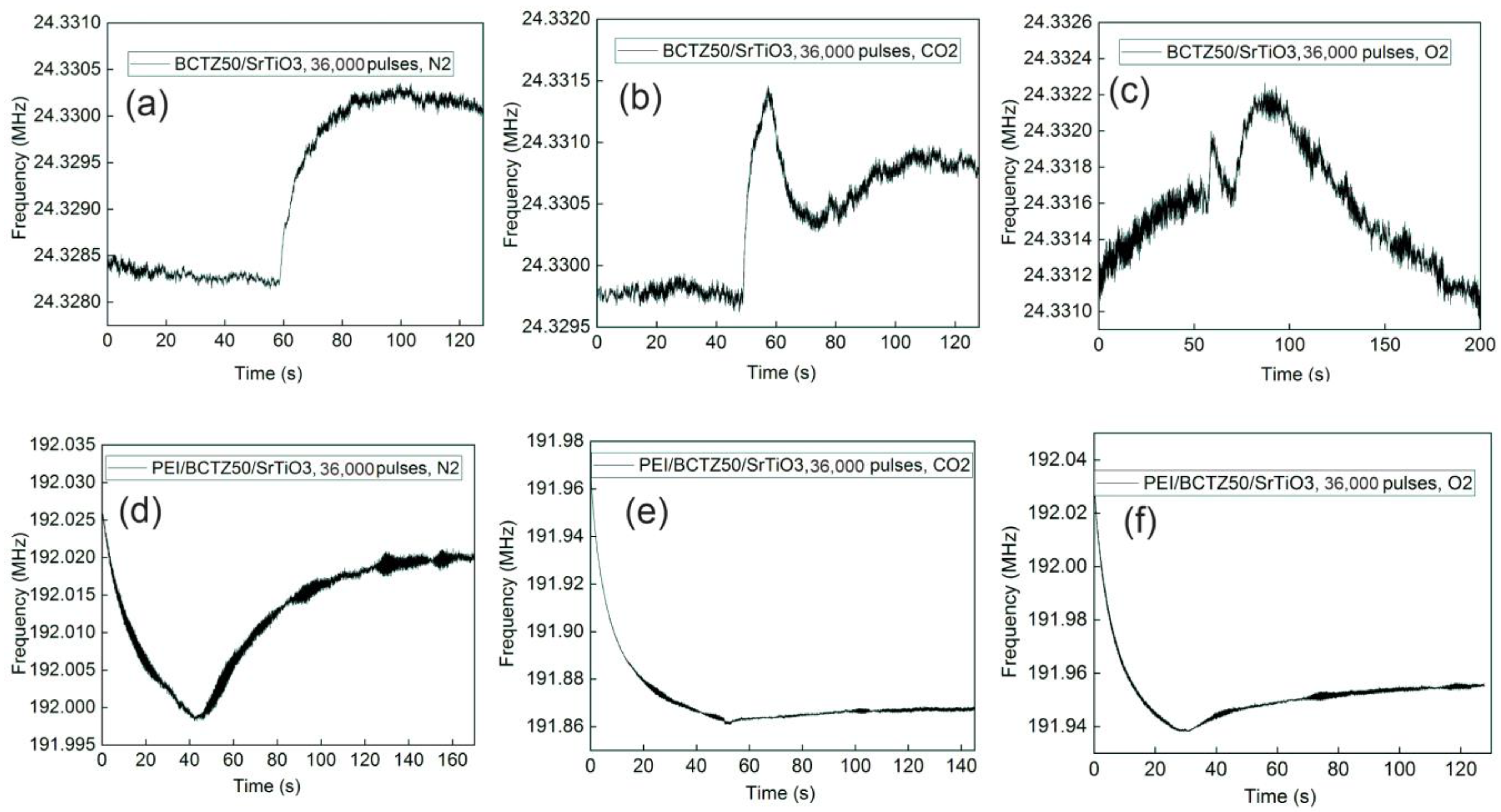
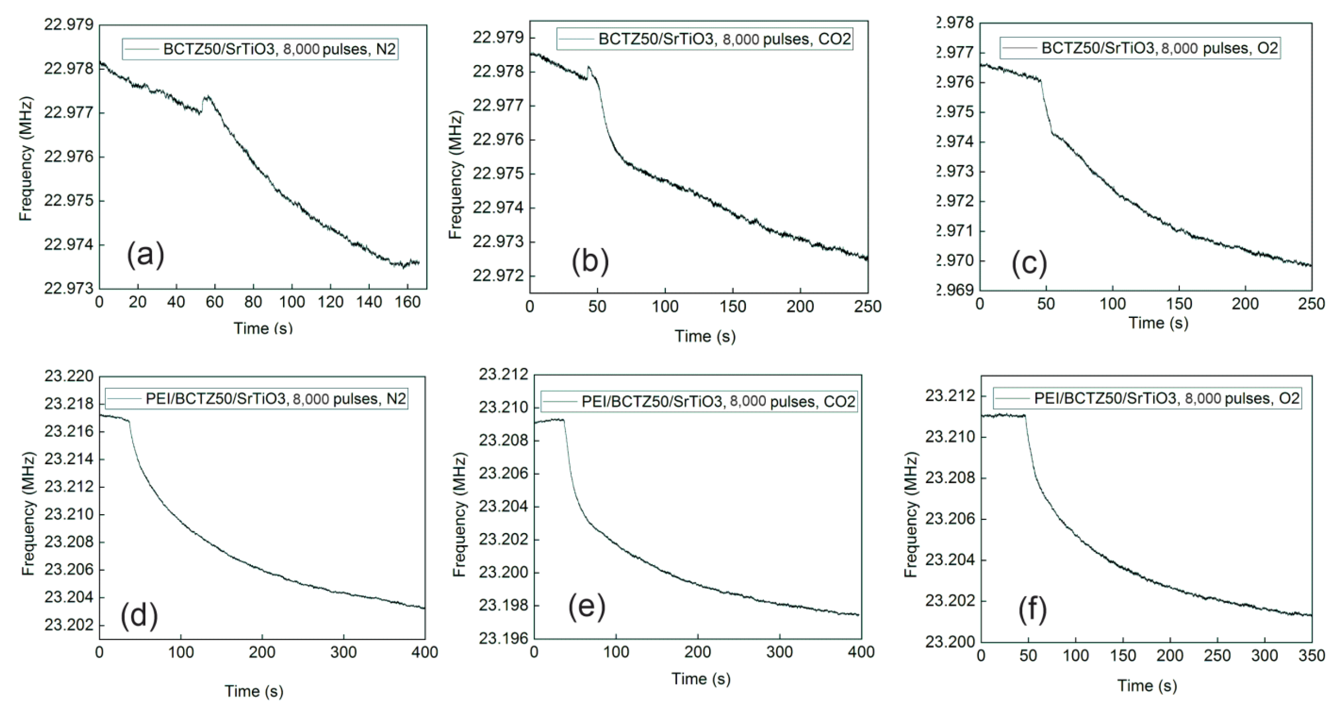
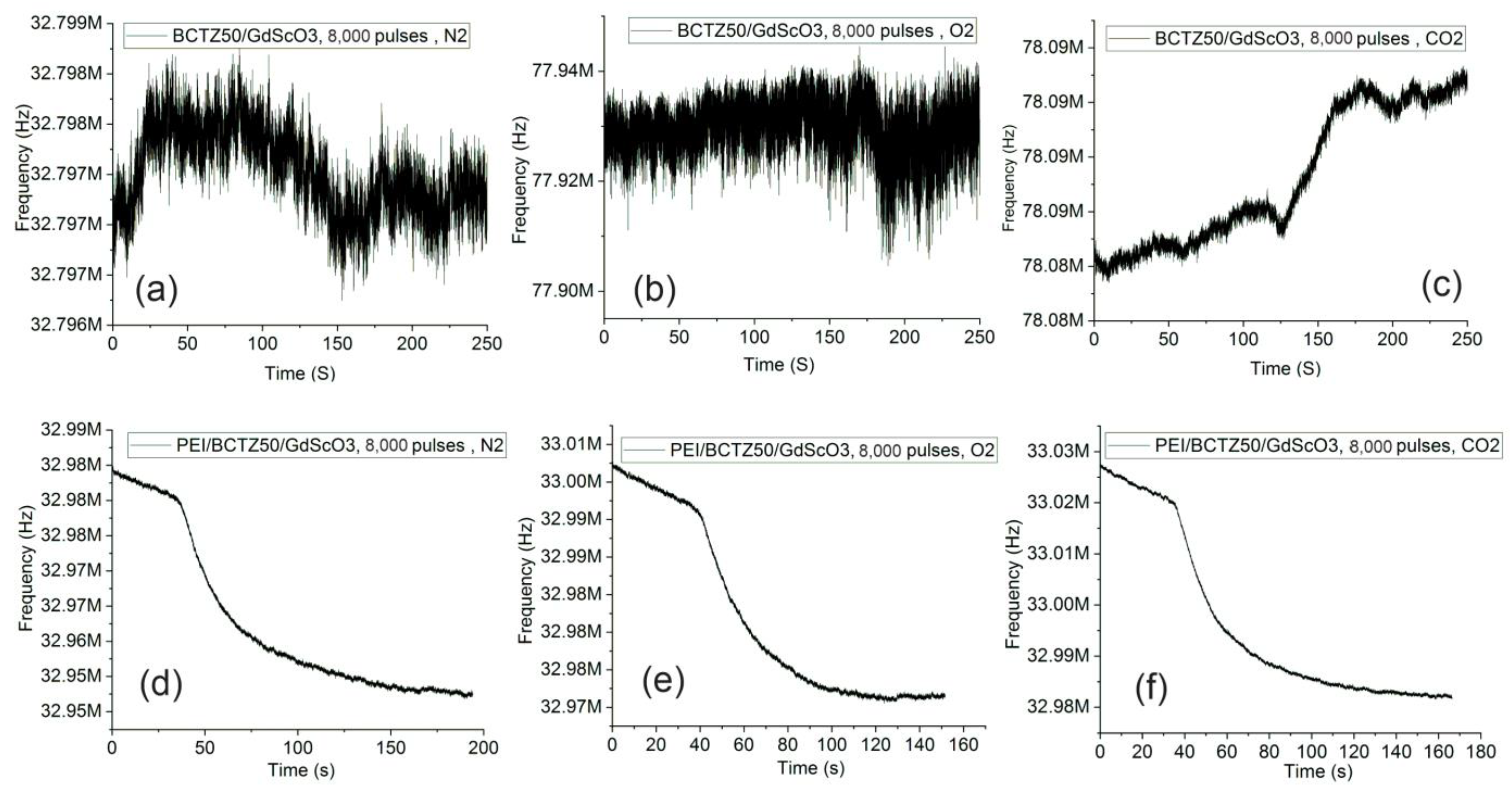
3.4. SAW Measurements

The SAW sensor testing system consisted of an amplifier and a frequency counter connected to a computer with specialised software (Figure 8). The gas flow was ensured by a mass flow controller through a mass flow meter.
The gases used for the tests were carbon dioxide (CO2), nitrogen (N2) and oxygen (O2), and the tests were carried out at a concentration of 99.996% N2, 99.999% O2, 99.998% CO2 and a gas flow of 500 sccm.
The first important aspect noted from the frequency shifts was that the sensors with a PEI-sensitive layer had a higher frequency shift than those without a polymeric layer. At the same time, the sensors based on BCTZ50 deposited on an SrTiO3 substrate had a small response or did not exhibit any response without the polymeric sensitive layer. A higher response was obtained for BCTZ50 deposited on a GdScO3 substrate with a frequency shift between 12–19 KHz (Figure 9). In the case of BCTZ50/SrTiO3, when the thickness was increased by a higher number of laser pulses, the response of the SAW sensor became unclear and very noise and we cannot accurately state the existence of a gas response (for example BCTZ50 deposited with 36,000 laser pulses in Figure 10). The test response from the PEI/BCTZ50/STO (8000 pulses), presented in Figure 11, sensor indicates a greater efficiency when testing for N2, with 12.66 kHz frequency shift, compared to responses of 9 kHz for O2 and 11.29 kHz for CO2.
The best results for the frequency shifts were obtained in the case of PEI/BCTZ50/GSO thin films. The highest frequency shift was about 39 kHz, obtained for O2 and CO2 gases by the PEI/BCTZ50/GSO-based SAW sensor. The values of the frequency shifts for these sensors were not contrasting, even when comparing different types of gases tested, which means that we cannot state if they are selective sensors.
The response time of the sensors was also influenced by the presence of the polymeric layer. Although we observed that, for BCTZ50/GSO sensors, the frequency shift was improved with the use of the polymeric coating, the influence on the response time was both increasing and decreasing. This increase in response time is explained by the fact that the adsorption of molecules at the level of the sensitive layer takes place more slowly than when gas molecules come into direct contact with the sensor substrate. However, considering that the frequency shift increases when using the polymer, an increase in the response time is allowed. The BCTZ50/GSO sensor, in the tests for CO2, obtained both a decrease in the response time and an increase in the frequency shift (Figure 9).
The mechanism of gas sensing was explained by Wang et al. [53]. When gas molecules interact with surface of an oxide, the charge state is altered, and the conductivity of sample is changed. A change in the conductivity of layer leads to a change in SAW sensor response. For all samples deposited with 8000 laser pulses, we calculated, from optical analysis, a percentage of pores around 6–8%. From Figure 10 and Figure 11, we can observe the response for BCTZ50/STO without a polymeric layer in the presence of two analysed gases (O2 and CO2). The presence of pores causes oxygen to be easily adsorbed and the high porosity provides a larger amount of surface sites for gas adsorption and chemical reactions [54]. This may attract more electrons from the BCTZ layer and substantially modify their frequency response in SAW measurement configuration. This behaviour in BaTiO3-based materials was already reported by Park et al. [55] in the case of Sb2O3-BaTiO3, and they showed the importance of porosity for gas response in the case of Sb2O3-BaTiO3. Moreover, other studies reported similar response behaviours for CO sensing, such as in the case of SnO2, which has higher sensitivities but a smaller grain size [56,57,58].
By ading a polymer layer (PEI in this case), the mecanism behind overall response was changed. This time, the gas molecules were absorbed by the PEI layer, and because BCTZ is a piezoelectric material, changing the mass of the polymeric cover layer induced a response in the BCTZ film. The frequency shifts in samples with a polimeric layer were around 9–11 KHz for CO2 and O2, and this is normal behavior for PEI [59].
When the number of laser pulses increased to 36,000 and the thickness of BCTZ50/STO layer increased more than three times, a strange behaviour was observed in the gas response. For N2 in the case of the BCTZ50/STO with a thickness of ~300 nm the frequency response was noisy, but when N2 was introduced in testing chamber, a shift was observed (Figure 10). For CO2 and O2 the shift was noticeable but weak and the frequency response became noisy and unstable in a matter of a few seconds after the gas was introduced. Even with PEI layer, the gas response was not clear. At high thicknesses, the properties of the BCTZ thin layer were similar to bulk BCTZ, and because there was no gas response for thicker BCTZ50/STO, we can conclude that this material is only suitable for gas detection when the functional properties are altered by structural strain.
In the case of BCTZ50 thin films deposited on GSO, the gas response as a function of thickness/strain relaxation was completely different in respect to the BCTZ50/STO films. For the thin, 8000 laser-pulsed BCTZ50/GSO sample without the PEI coating, only a weak response in the presence of CO2 was noticed. For the BCTZ 50/GSO thin films, the frequency measured during time before and after gas was introduced to the chamber are presented in Figure 12 and Figure 13. For the thickest BCTZ50/GSO sample, a good response was noted without the polymer layer for all analysed gases, with a frequency shift between 12 and 39 KHz. The best response time for the thick BCTZ50/GSO sample was around 80 s in the case of oxygen gas detection. By adding a polymer layer, the frequency shift was increased to ~50 KHz; a higher frequency shift translated into a better response for all gases, but for CO2, the response time was also increased a few times. The highest response time can be explained by a slow chemical reaction between the polymer and the gas molecules.
The difference between the gas responses from BCTZ deposited on different substrates were clearly observable, and in close correlation with crystalline features of the samples. As the in-plane strain-ɛ (%) in the BCTZ50/GSO samples is much smaller than in the case of the BCTZ50/STO samples, combined with the improved moisaicity (FWHM-ω(002)), it is clear that the less-structurally defective BCTZ50/GSO films are suitable for acoustic wave propagation within the films in contrast with the BCTZ50/STO ones.

4. Conclusions

Here, gas sensing performance as a function of thickness and substrate variation in BCTZ50 and PEI/BCTZ50 thin films deposited by laser-based techniques, in correlation with morphological, structural and optical characteristics, has been presented. BCTZ50 samples with different thicknesses were deposited on two types of substrates with different crystal structures, cubic (SrTiO3) and orthorhombic (GdScO3). Spectrometric ellipsometry investigations revealed that, when the sample thickness increased, the thin film relaxed, and the optical properties were found to be similar with bulk BCTZ. The values of the GSO extinction coefficients were found to be higher for samples grown on STO, and the difference between optical constants values for samples grown on different substrates can be explained by the crystallinity of thin films, induced by the substrate during the PLD deposition process. After depositing IDT Au electrodes, the thin films were integrated into SAW devices in order to measure the frequency response to various gases (N2, CO2 and O2). The response of BCTZ50 and PEI/BCTZ50 sensors was evaluated. The first important aspect noted from the frequency shifts was that the sensors with a PEI-sensitive layer had a higher frequency shift than those without a polymeric layer. At the same time, the sensors based on BCTZ50 and deposited with 8000 laser pulses on a SrTiO3 substrate did not have such a high response without a polymeric sensitive layer. The test response of the BCTZ50/GSO sensor was 17.6 kHz with PEI and 19.1 kHz without PEI, indicating a greater efficiency when testing for N2. The best efficiency when testing for O2 was recorded for PEI/BCTZ50, with a value of 39.5 kHz, more than two times higher compared to the film without the polymeric layer. The best results of the frequency shifts were obtained by the PEI/BCTZ50 sensors deposited on GdScO3; this was also the best when detecting CO2, with a recorded frequency shift of 39 kHz. In the case of CO2 detection, when using PEI, the frequency shift increase was more than three times recorded for bare BCTZ50/GSO. The response time of the sensors was also influenced by the presence or absence of the polymeric layer, noting an increase in the response time when using PEI. This behaviour resulted from the fact that the adsorption of molecules at the level of the sensitive layer takes place more slowly than when gas molecules come into direct contact with the sensor substrate, thus an increase in the response time with an increase in the frequency shift is acceptable.

Author Contributions

Conceptualization, N.E., V.I., C.V. and N.D.S.; PLD and MAPLE experiments N.E. and M.L.S.; investigation, N.E., V.I., A.B., I.C., R.B. and C.V.; writing—original draft preparation, N.E. and V.I.; writing—review and editing, N.E., V.I. and N.D.S.; supervision, N.D.S.; funding acquisition, V.I. and N.D.S. All authors have read and agreed to the published version of the manuscript.

Funding

This work was supported by a grant of the Romanian Ministry of Education and Research, CCCDI–UEFISCDI, project number PN-III-P2-2.1-PED-2019-4734, within PNCDI III.

Data Availability Statement

The data presented in this study are available on request from the corresponding author.

Acknowledgments

The authors would like to acknowledge the contribution of Cristina Craciun for AFM investigations. SEM images were obtained using C400 PHOTOPLASMAT facilities ac-quired within the POC153/2016 IN2-FOTOPLASMAT project.

Conflicts of Interest

The authors declare no conflicts of interest.

References

  1. Wang, J.L.; Guo, Y.J.; Long, G.D.; Tang, Y.L.; Tang, Q.B.; Zu, X.T.; Ma, J.Y.; Du, B.; Torun, H.; Fu, Y.Q. Integrated sensing layer of bacterial cellulose and polyethyleneimine to achieve high sensitivity of ST-cut quartz surface acoustic wave formaldehyde gas sensor. J. Hazard. Mater. 2020, 388, 121743. [Google Scholar] [CrossRef] [PubMed]
  2. Wang, W.; Liu, X.; Mei, S.; Jia, Y.; Liu, M.; Xue, X.; Yang, D. Development of a Pd/Cu nanowires coated SAW hydrogen gas sensor with fast response and recovery. Sens. Actuators B Chem. 2019, 287, 157–164. [Google Scholar] [CrossRef]
  3. Rana, L.; Gupta, R.; Kshetrimayum, R.; Tomar, M.; Gupta, V. Fabrication of surface acoustic wave based wireless NO2 gas sensor. Surf. Coat. Technol. 2018, 343, 89–92. [Google Scholar] [CrossRef]
  4. Ghosh, A.; Zhang, C.; Shi, S.; Zhang, H. High temperature CO2 sensing and its cross-sensitivity towards H2 and CO gas using calcium doped ZnO thin film coated langasite SAW sensor. Sens. Actuators B Chem. 2019, 301, 126958. [Google Scholar] [CrossRef]
  5. Tang, Y.; Li, D.; Ao, D.; Guo, Y.; Faheem, M.B.; Khan, B.; Zu, X.; Li, S. Highly sensitive surface acoustic wave HCl gas sensors based on hydroxyl-rich sol-gel AlOxOHy films. Mater. Chem. Phys. 2020, 239, 122026. [Google Scholar] [CrossRef]
  6. Shu, L.; Jiang, T.; Xia, Y.; Wang, X.; Yan, D.; Wu, W. The Investigation of a SAW Oxygen Gas Sensor Operated at Room Temperature, Based on Nanostructured ZnxFeyO Films. Sensors 2019, 19, 3025. [Google Scholar] [CrossRef] [PubMed]
  7. Constantinoiu, I.; Miu, D.; Viespe, C. Surface Acoustic Wave Sensors for Ammonia Detection at Room Temperature Based on SnO2/Co3O4 Bilayers. J. Sens. 2019, 2019, 8203810. [Google Scholar] [CrossRef]
  8. Yang, L.; Yin, C.; Zhang, Z.; Zhou, J.; Xu, H. The investigation of hydrogen gas sensing properties of SAW gas sensor based on palladium surface modified SnO2 thin film. Mater. Sci. Semicond. Process. 2017, 60, 16–28. [Google Scholar] [CrossRef]
  9. Tang, Y.; Xu, X.; Han, S.; Cai, C.; Du, H.; Zhu, H.; Zu, X.; Fu, Y. ZnO-Al2O3 nanocomposite as a sensitive layer for high performance surface acoustic wave H2S gas sensor with enhanced elastic loading effect. Sens. Actuators B Chem. 2020, 304, 127395. [Google Scholar] [CrossRef]
  10. Lim, J.-B.; Reddeppa, M.; Nam, D.; Pasupuleti, K.S.; Bak, N.-H.; Kim, S.-G.; Cho, H.D.; Kim, M.-D. Surface acoustic device for high response NO2 gas sensor using p-phenylenediamine-reduced graphene oxide nanocomposite coated on langasite. Smart Mater. Struct. 2021, 30, 095016. [Google Scholar] [CrossRef]
  11. Devkota, J.; Ohodnicki, P.; Greve, D. SAW Sensors for Chemical Vapors and Gases. Sensors 2017, 17, 801. [Google Scholar] [CrossRef] [PubMed]
  12. Khlebarov, Z.P.; Stoyanova, A.I.; Topalova, D.I. Surface acoustic wave gas sensors. Sens. Actuators B Chem. 1992, 8, 33–40. [Google Scholar] [CrossRef]
  13. Shen, C.-Y.; Huang, C.-P.; Huang, W.-T. Gas-detecting properties of surface acoustic wave ammonia sensors. Sens. Actuators B Chem. 2004, 101, 1–7. [Google Scholar] [CrossRef]
  14. Caliendo, C.; Verardi, P.; Verona, E.; D’Amico, A.; Natale, C.D.; Saggio, G.; Serafini, M.; Paolesse, R.; Huq, S.E. Advances in SAW-based gas sensors. Smart Mater. Struct. 1997, 6, 689–699. [Google Scholar] [CrossRef]
  15. Midhuna, A.S.; Shiju, B.S.; Sreenidhi, P.R. Optimizing Design of Surface Acoustic Wave Gas Sensor. In Proceedings of the 2021 5th International Conference on Trends in Electronics and Informatics (ICOEI), Tirunelveli, India, 3–5 June 2021; pp. 143–148. [Google Scholar] [CrossRef]
  16. Liu, B.; Chen, X.; Cai, H.; Mohammad Ali, M.; Tian, X.; Tao, L.; Yang, Y.; Ren, T. Surface acoustic wave devices for sensor applications. J. Semicond. 2016, 37, 021001. [Google Scholar] [CrossRef]
  17. Jakubik, W.P. Surface acoustic wave-based gas sensors. Thin Solid Films 2011, 520, 986–993. [Google Scholar] [CrossRef]
  18. Hamidon, M.N.; Yunusa, Z. Sensing Materials for Surface Acoustic Wave Chemical Sensors. In Progresses in Chemical Sensor; Wang, W., Ed.; InTech: Vienna, Austria, 2016. [Google Scholar] [CrossRef]
  19. Liu, X.; Cheng, S.; Liu, H.; Hu, S.; Zhang, D.; Ning, H. A Survey on Gas Sensing Technology. Sensors 2012, 12, 9635–9665. [Google Scholar] [CrossRef] [PubMed]
  20. Luo, W.; Fu, Q.; Zhou, D.; Deng, J.; Liu, H.; Yan, G. A surface acoustic wave H2S gas sensor employing nanocrystalline SnO2 thin film. Sens. Actuators B Chem. 2013, 176, 746–752. [Google Scholar] [CrossRef]
  21. Dickert, F.L.; Forth, P.; Bulst, W.-E.; Fischerauer, G.; Knauer, U. SAW devices-sensitivity enhancement in going from 80 MHz to 1 GHz. Sens. Actuators B Chem. 1998, 46, 120–125. [Google Scholar] [CrossRef]
  22. Sayago, I.; Fernandez, M.J.; Fontecha, J.L.; Horrillo, M.C.; Terrado, E.; Seral-Ascaso, A.; Munoz, E. Carbon nanotube-based SAW sensors. In Proceedings of the 2013 Spanish Conference on Electron Devices, Valladolid, Spain, 12–14 February 2013; IEEE: Valladolid, Spain, 2013; pp. 127–130. [Google Scholar] [CrossRef]
  23. Sayago, I.; Fernández, M.J.; Fontecha, J.L.; Horrillo, M.C.; Vera, C.; Obieta, I.; Bustero, I. New sensitive layers for surface acoustic wave gas sensors based on polymer and carbon nanotube composites. Sens. Actuators B Chem. 2012, 175, 67–72. [Google Scholar] [CrossRef]
  24. Asad, M.; Sheikhi, M.H. Surface acoustic wave based H2S gas sensors incorporating sensitive layers of single wall carbon nanotubes decorated with Cu nanoparticles. Sens. Actuators B Chem. 2014, 198, 134–141. [Google Scholar] [CrossRef]
  25. Xu, S.; Li, C.; Li, H.; Li, M.; Qu, C.; Yang, B. Carbon dioxide sensors based on a surface acoustic wave device with a graphene–nickel– L -alanine multilayer film. J. Mater. Chem. C 2015, 3, 3882–3890. [Google Scholar] [CrossRef]
  26. Wang, S.-H.; Shen, C.-Y.; Su, J.-M.; Chang, S.-W. A Room Temperature Nitric Oxide Gas Sensor Based on a Copper-Ion-Doped Polyaniline/Tungsten Oxide Nanocomposite. Sensors 2015, 15, 7084–7095. [Google Scholar] [CrossRef] [PubMed]
  27. Sadek, A.Z.; Wlodarski, W.; Shin, K.; Kaner, R.B.; Kalantar-zadeh, K. A layered surface acoustic wave gas sensor based on a polyaniline/In2O3 nanofibre composite. Nanotechnology 2006, 17, 4488–4492. [Google Scholar] [CrossRef]
  28. Sil, D.; Hines, J.; Udeoyo, U.; Borguet, E. Palladium Nanoparticle-Based Surface Acoustic Wave Hydrogen Sensor. ACS Appl. Mater. Interfaces 2015, 7, 5709–5714. [Google Scholar] [CrossRef]
  29. Robinson, A.L.; Stavila, V.; Zeitler, T.R.; White, M.I.; Thornberg, S.M.; Greathouse, J.A.; Allendorf, M.D. Ultrasensitive Humidity Detection Using Metal–Organic Framework-Coated Microsensors. Anal. Chem. 2012, 84, 7043–7051. [Google Scholar] [CrossRef] [PubMed]
  30. Tasaltin, C.; Ebeoglu, M.A.; Ozturk, Z.Z. Acoustoelectric Effect on the Responses of SAW Sensors Coated with Electrospun ZnO Nanostructured Thin Film. Sensors 2012, 12, 12006–12015. [Google Scholar] [CrossRef]
  31. Kumar, A.; Prajesh, R. The potential of acoustic wave devices for gas sensing applications. Sens. Actuators Phys. 2022, 339, 113498. [Google Scholar] [CrossRef]
  32. Omori, T.; Hashimoto, K.; Yamaguchi, M. PZT Thin Films for SAW and BAW Devices, Engineering, Materials Science, Physics, Department of Electronics and Mechanical Engineering, Chiba University Inage-ku, Chiba-shi, 263-8522, Japan. Available online: https://www.te.chiba-u.jp/lab/ken/Symp/Symp2001/PAPER/OMORI.PDF (accessed on 27 October 2022).
  33. Hsiao, Y.-J.; Fang, T.-H.; Chang, Y.-H.; Chang, Y.-S.; Wu, S. Surface acoustic wave characteristics and electromechanical coupling coefficient of lead zirconate titanate thin films. Mater. Lett. 2006, 60, 1140–1143. [Google Scholar] [CrossRef]
  34. Shilpa, G.D.; Sreelakshmi, K.; Ananthaprasad, M.G. PZT thin film deposition techniques, properties and its application in ultrasonic MEMS sensors: A review. IOP Conf. Ser. Mater. Sci. Eng. 2016, 149, 012190. [Google Scholar] [CrossRef]
  35. Takenaka, T. Lead-free piezo-ceramics. In Advanced Piezoelectric Materials; Elsevier: Amsterdam, The Netherlands, 2010; pp. 130–170. [Google Scholar] [CrossRef]
  36. Jaffe, W.R.C.B.; Jaffe, H. Piezoelectric Ceramics, 1st ed.; Academic Press: Cambridge, MA, USA, 1971. [Google Scholar]
  37. Liu, W.; Ren, X. Large Piezoelectric Effect in Pb-Free Ceramics. Phys. Rev. Lett. 2009, 103, 257602. [Google Scholar] [CrossRef] [PubMed]
  38. Gao, J.; Xue, D.; Liu, W.; Zhou, C.; Ren, X. Recent Progress on BaTiO3-Based Piezoelectric Ceramics for Actuator Applications. Actuators 2017, 6, 24. [Google Scholar] [CrossRef]
  39. Li, W.L.; Zhang, T.D.; Xu, D.; Hou, Y.F.; Cao, W.P.; Fei, W.D. LaNiO3 seed layer induced enhancement of piezoelectric properties in (100)-oriented (1−x)BZT–xBCT thin films. J. Eur. Ceram. Soc. 2015, 35, 2041–2049. [Google Scholar] [CrossRef]
  40. Li, W.L.; Zhang, T.D.; Hou, Y.F.; Zhao, Y.; Xu, D.; Cao, W.P.; Fei, W.D. Giant piezoelectric properties of BZT–0.5BCT thin films induced by nanodomain structure. RSC Adv. 2014, 4, 56933–56937. [Google Scholar] [CrossRef]
  41. Scarisoreanu, N.D.; Craciun, F.; Moldovan, A.; Ion, V.; Birjega, R.; Ghica, C.; Negrea, R.F.; Dinescu, M. High Permittivity (1 − x)Ba(Zr0.2Ti0.8)O3x (Ba0.7Ca0.3)TiO3 (x = 0.45) Epitaxial Thin Films with Nanoscale Phase Fluctuations. ACS Appl. Mater. Interfaces 2015, 7, 23984–23992. [Google Scholar] [CrossRef] [PubMed]
  42. Yan, Y.; Yang, G.; Xu, J.-L.; Zhang, M.; Kuo, C.-C.; Wang, S.-D. Conducting polymer-inorganic nanocomposite-based gas sensors: A review. Sci. Technol. Adv. Mater. 2020, 21, 768–786. [Google Scholar] [CrossRef] [PubMed]
  43. Fratoddi, I.; Venditti, I.; Cametti, C.; Russo, M.V. Chemiresistive polyaniline-based gas sensors: A mini review. Sens. Actuators B Chem. 2015, 220, 534–548. [Google Scholar] [CrossRef]
  44. Bartlett, P.N.; Archer, P.B.M.; Ling-Chung, S.K. Conducting polymer gas sensors part I: Fabrication and characterization. Sens. Actuators 1989, 19, 125–140. [Google Scholar] [CrossRef]
  45. Dinca, V.; Viespe, C.; Brajnicov, S.; Constantinoiu, I.; Moldovan, A.; Bonciu, A.; Toader, C.; Ginghina, R.; Grigoriu, N.; Dinescu, M.; et al. MAPLE Assembled Acetylcholinesterase–Polyethylenimine Hybrid and Multilayered Interfaces for Toxic Gases Detection. Sensors 2018, 18, 4265. [Google Scholar] [CrossRef]
  46. Regensburger, S.; Mohammadi, M.; Khawaja, A.A.; Radetinac, A.; Komissinskiy, P.; Alff, L.; Preu, S. Optical Properties of Highly Conductive SrMoO3 Oxide Thin Films in the THz Band and Beyond. J. Infrared Millim. Terahertz Waves 2020, 41, 1170–1180. [Google Scholar] [CrossRef]
  47. Scarisoreanu, N.D.; Craciun, F.; Birjega, R.; Ion, V.; Teodorescu, V.S.; Ghica, C.; Negrea, R.; Dinescu, M. Joining Chemical Pressure and Epitaxial Strain to Yield Y-doped BiFeO3 Thin Films with High Dielectric Response. Sci. Rep. 2016, 6, 25535. [Google Scholar] [CrossRef] [PubMed]
  48. Metzger, T.; Höpler, R.; Born, E.; Ambacher, O.; Stutzmann, M.; Stömmer, R.; Schuster, M.; Göbel, H.; Christiansen, S.; Albrecht, M.; et al. Defect structure of epitaxial GaN films determined by transmission electron microscopy and triple-axis X-ray diffractometry. Philos. Mag. A 1998, 77, 1013–1025. [Google Scholar] [CrossRef]
  49. Schwarzkopf, J.; Braun, D.; Schmidbauer, M.; Duk, A.; Wördenweber, R. Ferroelectric domain structure of anisotropically strained NaNbO3 epitaxial thin films. J. Appl. Phys. 2014, 115, 204105. [Google Scholar] [CrossRef]
  50. Spectroscopic Ellipsometry: Principles and Applications|Wiley. Available online: https://www.wiley.com/en-us/Spectroscopic+Ellipsometry%3A+Principles+and+Applications-p-9780470016084 (accessed on 27 October 2022).
  51. Liu, D.; Shim, J.; Sun, Y.; Li, Q.; Yan, Q. Growth of Ca, Zr co-doped BaTiO3 lead-free ferroelectric single crystal and its room-temperature piezoelectricity. AIP Adv. 2017, 7, 095311. [Google Scholar] [CrossRef]
  52. Wemple, S.H.; Didomenico, M.; Camlibel, I. Dielectric and optical properties of melt-grown BaTiO3. J. Phys. Chem. Solids 1968, 29, 1797–1803. [Google Scholar] [CrossRef]
  53. Santhosh Kumar, T.; Bhuyan, R.K.; Pamu, D. Effect of post annealing on structural, optical and dielectric properties of MgTiO3 thin films deposited by RF magnetron sputtering. Appl. Surf. Sci. 2013, 264, 184–190. [Google Scholar] [CrossRef]
  54. Wang, C.; Yin, L.; Zhang, L.; Xiang, D.; Gao, R. Metal Oxide Gas Sensors: Sensitivity and Influencing Factors. Sensors 2010, 10, 2088–2106. [Google Scholar] [CrossRef]
  55. Park, K.; Seo, D.J. Gas sensing characteristics of BaTiO3-based ceramics. Mater. Chem. Phys. 2004, 85, 47–51. [Google Scholar] [CrossRef]
  56. Li, F.; Xu, J.; Yu, X.; Chen, L.; Zhu, J.; Yang, Z.; Xin, X. One-step solid-state reaction synthesis and gas sensing property of tin oxide nanoparticles. Sens. Actuators B Chem. 2002, 81, 165–169. [Google Scholar] [CrossRef]
  57. Yamazoe, N. New approaches for improving semiconductor gas sensors. Sens. Actuators B Chem. 1991, 5, 7–19. [Google Scholar] [CrossRef]
  58. Van Toan, N.; Viet Chien, N.; Van Duy, N.; Si Hong, H.; Nguyen, H.; Duc Hoa, N.; Van Hieu, N. Fabrication of highly sensitive and selective H2 gas sensor based on SnO2 thin film sensitized with microsized Pd islands. J. Hazard. Mater. 2016, 301, 433–442. [Google Scholar] [CrossRef]
  59. Sun, B.; Xie, G.; Jiang, Y.; Li, X. Comparative CO2-Sensing Characteristic Studies of PEI and PEI/Starch Thin Film Sensors. Energy Procedia 2011, 12, 726–732. [Google Scholar] [CrossRef]
Figure 1. SEM images of thin films deposited on (STO) heated at 700 °C in mbar of oxygen (a) BCTZ50/STO; (b) PEI/BCTZ50/STO; (c) BCTZ50/GSO and (d) PEI/BCTZ50/GSO.
Nanomaterials 14 00039 g001
Figure 2. AFM topography images for 36,000 laser pulses BCTZ thin films (a) BCTZ50/GSO (b) BCTZ50/STO and (c) PEI/BCTZ50/STO.
Nanomaterials 14 00039 g002
Figure 3. XRD patterns of the BCZT. (a) BCTZ standard card ICDID card no. 00-063-0614 and BCTZ50 target; (b) thin films deposited on GSO with 8000 laser pulses; (c) thin films deposited on STO with 36,000 laser pulses.
Nanomaterials 14 00039 g003
Figure 4. XRD four-circle Φ scans around (101) BCZT reflection for (a,b) BCTZ/STO films with different thickness and (c,d) BCTZ/GSO films with different thickness.
Nanomaterials 14 00039 g004
Figure 5. XRD X-ray rocking curves (ω-scans) of the BCZT (002) reflections for the films deposited on STO and GSO substrates.
Nanomaterials 14 00039 g005
Figure 6. Comparison between the dispersion of optical constants for the BCTZ50/STO thin layer growth at 8000 and 36,000 laser pulses: (a) refractive index and (b) extinction coefficients. In caption zoom of refractive index for samples in UV spectral region
Nanomaterials 14 00039 g006
Figure 7. The values of optical constants for the BCTZ50 thin layers deposited on GdScO3 substrate at (a) 8000 and (b) 36,000 laser pulses: (a) refractive index and (b) extinction coefficients. In caption zoom of exctinction coefficients for samples in UV spectral region
Nanomaterials 14 00039 g007
Figure 8. Experimental setup for SAW sensor frequency shift measurements.
Nanomaterials 14 00039 g008
Figure 9. The frequency shift of BCTZx sensors at different gases.
Nanomaterials 14 00039 g009
Figure 10. The gas response for the BCTZ50 deposited on SrTiO3 substrate by PLD with 36,000 laser pulses without polymers for (a) N2; (b) CO2; (c) O2; and PEI/BCTZ50 for (d) N2; (e) CO2; (f) O2.
Nanomaterials 14 00039 g010
Figure 11. The gas response for the BCTZ50 deposited on SrTiO3 substrate by PLD with 8000 laser pulses without polymers for (a) N2; (b) CO2; (c) O2; and BCTZ50 with PEI polymer for (d) N2; (e) CO2; (f) O2.
Nanomaterials 14 00039 g011
Figure 12. The gas response for the BCTZ50 deposited on GdScO3 substrate by PLD with 8000 laser pulses without polymer for (a) N2; (b) CO2; (c) O2; and PEI/BCTZ50 for (d) N2; (e) CO2; (f) O2.
Nanomaterials 14 00039 g012
Figure 13. The gas response for the BCTZ50 deposited on GdScO3 substrate by PLD with 36,000 laser pulses without polymer for (a) N2; (b) CO2; (c) O2 and PEI/BCTZ50 for (d) N2; (e) CO2; (f) O2.
Nanomaterials 14 00039 g013
Table 1. Structural data extracted from XRD analysis.
ProbeLaser Pulsesaout-of-plane (Å)ain-plane (Å)In-Plane Strain-ε in-plane (%)FWHM-ω(002)(deg)LII (nm)αtilt (deg)
BCZT50/STO80004.01934.01732.880.068720.227
BCZT50/GSO80004.10223.97990.330.0562700.096
BCZT50/STO36,0004.01523.98572.070.0783760.051
BCZT50/GSO36,0004.01624.01471.200.0314710.054
Table 2. The values of thicknesses and the Gauss parameters for the BCTZ samples growth by PLD.
ProbeLaser PulsesThickness
(nm)
Roughness
(nm)
Amp
Gauss
En
(eV)
Br
(eV)
MSE
BCTZ 50/STO800093.32.19.314.701.022.777
BCTZ 50/STO36,000314.91.312.294.931.121.374
BCTZ 50/GSO800067.22.811.394.921.172.803
BCTZ 50/GSO36,000340.19.111.944.891.088.395
Table 3. The packing density and porosity for samples of BCTZx deposited by PLD on monocrystalline substrate.
ProbeLaser PulsesRefractive Index
(λ = 600 nm)
Packing DensityPorosity (%)
BCTZ50/GSO80002.330.9618.8
BCTZ 50/STO80002.3350.9668.34
BCTZ 50/STO36,0002.3320.9638.62
BCTZ 50/GSO36,0002.3110.95610.62
Disclaimer/Publisher’s Note: The statements, opinions and data contained in all publications are solely those of the individual author(s) and contributor(s) and not of MDPI and/or the editor(s). MDPI and/or the editor(s) disclaim responsibility for any injury to people or property resulting from any ideas, methods, instructions or products referred to in the content.

