
CMOS Scaling for the 5 nm Node and Beyond: Device, Process and Technology

 , , ,
, , ,  , , , add
Show full author list
, , , add
Show full author list
Abstract
1. Introduction
| Part I: Nanoscale tranisitor designs | The designs of Nanoscale Transistors in Approach to the End of Technology Roadmap and Beyond Moore |
| Advanced TCAD with AI for the 5 nm node and beyond | |
| Part II: Process of Nanoscale FETs | Advanced Lithography Technique |
| Epitaxy in Transistor Structures | |
| Implantation and Advanced Doping Methods | |
| HKMG, ALD Technique and Negative Capacitance Materials | |
| Advanced Etchning for Nano-Transistor Structures | |
| Wet Etch and Cleaning | |
| Metal Materials Interconnect | |
| Advanced Devices Reliability | |
| Part III: Materials in Beyond Moore Era | III–V Materials |
| Substrate Engineering (GOI and GeSnOI) | |
| Beyond Moore Era-Si Optoelectronics | |
| Part IV: Metrology technology | Advanced Material and Structural Analysis of Miniaturized CMOS |
2. The Designs of Nanoscale Transistors in Approach to the End of Technology Roadmap and beyond Moore
2.1. Novel Structure, Gate-All-Around FETs
2.2. Tunneling Field-Effect Transistor (TFET) Approach
2.3. FDSOI Technology
2.3.1. What Is FDSOI (Architectures and Characteristics)
2.3.2. FDSOI Salient Characteristics
2.3.3. FDSOI Roadmap and Future Perspectives
3. Advanced TCAD with AI for the 5 nm Node and beyond
3.1. Atomistic Calculation with AI
3.2. Semiclassical Device Simulation with AI
3.3. Compact Modeling with AI
4. Advanced Lithography Technique
- (1)
- Wavelength reduction: i-line (365 nm), DUV KrF (248 nm), DUV ArF (193 nm), and EUV (13.5 nm).
- (2)
- DUV NA increase: from 0.93 of ArF dry tool to 1.35 of ArF immersion at 193 nm lithographic tools.
- (3)
- EUV NA increase: from 0.33 to 0.5 at current EUV tool and future high-NA EUV tools.
- (4)
- K1 reduction through various patterning enhancement techniques (PETs).
4.1. EUV in Mass Production
4.2. Overlay and Edge Placement Error (EPE) Challenges
5. Epitaxy in Transistor Structures
5.1. Selective Epitaxy Growth (SEG) of SiGe in S/D Regions
5.2. Epitaxy of GeSi and Ge for Channel Region
5.3. Growth of SiGe/Si for Gate-All-Around (GAA) Structures
Different Novel Epitaxial Si/SiGe Is Used as Channel to Boost the Device Performance
6. Implantation and Advanced Doping Methods
6.1. Plasma Doping
6.2. Solid-State Diffusion
7. HKMG, ALD Technique and Negative Capacitance Materials
8. Advanced Etching for Nano-Transistor Structures
8.1. Dry Etching for 3D Transistor
8.2. Precise Etching: Atomic Layer Etching (ALE)
9. Wet Etch and Cleaning
10. Metal Materials Interconnect
11. Advanced Devices Reliability
12. III–V Materials
13. Substrate Engineering (GOI and GeSnOI)
13.1. Growth of GeSnOI Substrates
13.2. GeSnOI Transistor
14. Beyond Moore Era-Si Optoelectronics
Optoelectronic Integration
15. Advanced Material and Structural Analysis of Miniaturized CMOS
15.1. Scanning Electron Microscopy (SEM)
15.2. Transmission/Scanning Transmission Electron Microscopy (TEM/STEM) Technology
15.3. X-ray Metrology
15.4. Raman Spectroscopy
15.5. Hybrid Metrology

16. Conclusions
Author Contributions
Funding
Data Availability Statement
Conflicts of Interest
References
- Radamson, H.H.; Zhu, H.; Wu, Z.; He, X.; Lin, H.; Liu, J.; Xiang, J.; Kong, Z.; Xiong, W.; Li, J.; et al. State of the art and future perspectives in advanced CMOS technology. Nanomaterials 2020, 10, 1555. [Google Scholar] [CrossRef]
- Radamson, H.H.; He, X.; Zhang, Q.; Liu, J.; Cui, H.; Xiang, J.; Kong, Z.; Xiong, W.; Li, J.; Gao, J.; et al. Miniaturization of CMOS. Micromachines 2021, 10, 293. [Google Scholar] [CrossRef]
- Radamson, H.; Simoen, E.; Luo, J.; Zhao, C. CMOS Past, Present and Future; Woodhead Publishing: Cambridge, UK, 2018; ISBN 9780081021392. [Google Scholar]
- Jebalin, B.K.; Ajayan, J.; Franklin, S.A.; Nirmal, D. A new Vertical C-shaped Silicon Channel Nanosheet FET with Stacked High-K Dielectrics for Low Power Applications. Silicon 2024, 16, 2659–2670. [Google Scholar]
- Rezgui, H.; Wang, Y.; Mukherjee, C.; Deng, M.; Maneux, C. Signature of electrothermal transport in 18nm vertical junctionless gate-all-around nanowire field effect transistors. J. Phys. D Appl. Phys. 2024. [Google Scholar] [CrossRef]
- Maheshwaram, S.; Manhas, S.K.; Kaushal, G.; Anand, B.; Singh, N. Vertical silicon nanowire gate-all-around field effect transistor-based nanoscale CMOS. IEEE Electron Device Lett. 2011, 32, 1011–1013. [Google Scholar] [CrossRef]
- Wang, G.; Qin, C.; Yin, H.; Luo, J.; Duan, N.; Yang, P.; Gao, X.; Yang, T.; Li, J.; Yan, J.; et al. Study of SiGe selective epitaxial process integration with high-k and metal gate for 16/14 nm nodes FinFET technology. Microelectron. Eng. 2016, 163, 49–54. [Google Scholar] [CrossRef]
- Yin, X.; Zhang, Y.; Zhu, H.; Wang, G.L.; Li, J.J.; Du, A.Y.; Li, C.; Zhao, L.H.; Huang, W.X.; Yang, H.; et al. Vertical Sandwich Gate-All-Around Field-Effect Transistors with Self-Aligned High-k Metal Gates and Small Effective Gate-Length Variation. IEEE Electron Device Lett. 2019, 41, 8–11. [Google Scholar] [CrossRef]
- Zhang, Y.; Ai, X.; Yin, X.; Zhu, H.; Yang, H.; Wang, G.L.; Li, J.J.; Du, A.Y.; Li, C.; Huang, W.X.; et al. Vertical Sandwich GAA FETs with Self-Aligned High-k Metal Gate Made by Quasi Atomic Layer Etching Process. IEEE Trans. Electron Devices 2021, 68, 2604–2610. [Google Scholar] [CrossRef]
- Kim, S.; Lee, K.; Lee, J.H.; Park, B.G.; Kwon, D. Gate-first negative capacitance field-effect transistor with self-aligned nickel-silicide source and drain. IEEE Trans. Electron Devices 2021, 68, 4754–4757. [Google Scholar] [CrossRef]
- Li, C.; Zhu, H.; Zhang, Y.; Wang, Q.; Yin, X.; Li, J.; Wang, G.; Kong, Z.; Ai, X.; Xie, L.; et al. First Demonstration of Novel Vertical Gate-All-Around Field-Effect-Transistors Featured by Self-Aligned and Replaced High-κ Metal Gates. Nano Lett. 2021, 21, 4730–4737. [Google Scholar] [CrossRef]
- Zhang, Q.; Zhang, Y.; Luo, Y.; Yin, H. New structure transistors for advanced technology node CMOS ICs. Natl. Sci. Rev. 2024, 11, nwae008. [Google Scholar] [CrossRef]
- Huang, W.; Zhu, H.; Zhang, Y.; Yin, X.; Ai, X.; Li, J.; Li, C.; Li, Y.; Xie, L.; Liu, Y.; et al. Ferroelectric Vertical Gate-All-Around Field-Effect-Transistors with High Speed, High Density, and Large Memory Window. IEEE Electron Device Lett. 2022, 43, 25–28. [Google Scholar] [CrossRef]
- Liu, M.; Schlykow, V.; Hartmann, J.M.; Knoch, J.; Grützmacher, D.; Buca, D.; Zhao, Q.T. Vertical Heterojunction Ge0.92 Sn0.08/Ge GAA Nanowire pMOSFETs: Low SS of 67 mV/dec, Small DIBL of 24 mV/V and Highest Gm,ext of 870 μS/μm. In Proceedings of the 2020 IEEE Symposium on VLSI Technology, Honolulu, HI, USA, 16–19 June 2020; pp. 1–2. [Google Scholar]
- Liu, M.; Scholz, S.; Mertens, K.; Bae, J.H.; Hartmann, J.M.; Knoch, J.; Buca, D.; Zhao, Q.T. First Demonstration of Vertical Ge0.92 Sn0.08/Ge and Ge GAA Nanowire pMOSFETs with Low SS of 66 mV/dec and Small DIBL of 35 mV/V. In Proceedings of the IEEE International Electron Devices Meeting (IEDM), San Francisco, CA, USA, 7–11 December 2019. [Google Scholar]
- Liu, M.; Scholz, S.; Hardtdegen, A.; Bae, J.H.; Hartmann, J.M.; Knoch, J.; Grützmacher, D.; Buca, D.; Zhao, Q.T. Vertical Ge Gate-All-Around Nanowire pMOSFETs With a Diameter Down to 20 nm. IEEE Electron Device Lett. 2020, 41, 533–536. [Google Scholar] [CrossRef]
- Liu, M.; Lentz, F.; Trellenkamp, S.; Hartmann, J.M.; Knoch, J.; Grützmacher, D.; Buca, D.; Zhao, Q.T. Diameter Scaling of Vertical Ge Gate All-Around Nanowire pMOSFETs. IEEE Trans. Electron Devices 2020, 67, 2988–2994. [Google Scholar] [CrossRef]
- Tomiok, K.; Motohisa, J. Scaling effect on vertical gate-all-around FETs using III–V NW-channels on Si. In Proceedings of the Silicon Nanoelectronics Workshop (SNW), Virtual, 13 June 2021; pp. 1–2. [Google Scholar]
- Thingujam, T.; Dai, Q.; Kim, E.; Lee, J.H. A Simulation Study on the Effects of Interface Charges and Geometry on Vertical GAA GaN Nanowire MOSFET for Low-Power Application. IEEE Access 2021, 9, 101447–101453. [Google Scholar] [CrossRef]
- Thingujam, T.; Son, D.H.; Kim, J.G.; Cristoloveanu, S.; Lee, J.H. Effects of Interface Traps and Self-Heating on the Performance of GAA GaN Vertical Nanowire MOSFET. IEEE Trans. Electron Devices 2020, 67, 816–821. [Google Scholar] [CrossRef]
- Appenzeller, J.; Lin, Y.M.; Knoch, J.; Avouris, P. Band-to-band tunneling in carbon nanotube field-effect transistors. Phys. Rev. Lett. 2004, 93, 196805. [Google Scholar] [CrossRef]
- Choi, W.Y.; Park, B.G.; Lee, J.D.; Liu, T.J.K. Tunneling field-effect transistors (TFETs) with subthreshold swing (SS) less than 60 mV/dec. IEEE Electron Device Lett. 2007, 28, 743–745. [Google Scholar] [CrossRef]
- Mayer, F.; Le Royer, C.; Damlencourt, J.F.; Romanjek, K.; Andrieu, F.; Tabone, C.; Previtali, B.; Deleonibus, S. Impact of SOI, Si1−x GexOI and GeOI substrates on CMOS compatible tunnel FET performance. In Proceedings of the 2008 IEEE International Electron Devices Meeting, San Francisco, CA, USA, 15–17 December 2008; pp. 1–5. [Google Scholar] [CrossRef]
- Kim, S.H.; Kam, H.; Hu, C.; Liu, T.J.K. Germanium-source tunnel field effect transistors with record high ION/IOFF. In Proceedings of the 2009 Symposium on VLSI Technology, Kyoto, Japan, 16–18 June 2009; pp. 178–179, ISBN 978-1-4244-3308-7. [Google Scholar]
- Jeon, K.; Loh, W.Y.; Patel, P.; Kang, C.Y.; Oh, J.; Bowonder, A.; Park, C.; Park, C.S.; Smith, C.; Majhi, P.; et al. Si tunnel transistors with a novel silicided source and 46 mV/dec swing. In Proceedings of the 2010 Symposium on VLSI Technology, Honolulu, HI, USA, 15–17 June 2010; pp. 121–122. [Google Scholar] [CrossRef]
- Gandhi, R.; Chen, Z.; Singh, N.; Banerjee, K.; Lee, S. Vertical Si-nanowire n-type tunneling FETs with low subthreshold swing (≤50 mV/decade) at room temperature. IEEE Electron Device Lett. 2011, 32, 437. [Google Scholar] [CrossRef]
- Richter, S.; Sandow, C.; Nichau, A.; Trellenkamp, S.; Schmidt, M.; Luptak, R.; Bourdelle, K.K.; Zhao, Q.T.; Mantl, S. Omega-Gated Silicon and Strained Silicon Nanowire Array Tunneling FETs. IEEE Electron Device Lett. 2012, 33, 1535–1537. [Google Scholar] [CrossRef]
- Huang, Q.; Huang, R.; Zhan, Z.; Wu, C.; Qiu, Y.; Wang, Y. Performance improvement of Si Pocket-Tunnel FET with steep subthreshold slope and high ION/IOFF ratio. In Proceedings of the 2012 IEEE 11th International Conference on Solid-State and Integrated Circuit Technology, Xi’an, China, 29 October–1 November 2012; pp. 1–3. [Google Scholar] [CrossRef]
- Huang, Q.; Huang, R.; Zhan, Z.; Qiu, Y.; Jiang, W.; Wu, C.; Wang, Y. A novel Si tunnel FET with 36 mV/dec subthreshold slope based on junction depleted-modulation through striped gate configuration. In Proceedings of the 2012 International Electron Devices Meeting, San Francisco, CA, USA, 10–13 December 2012. [Google Scholar] [CrossRef]
- Liu, Y.; Wang, H.J.; Yan, J.; Han, G.Q. A Silicon Tunnel Field-Effect Transistor with an In Situ Doped Single Crystalline Ge Source for Achieving Sub-60 mV/decade Subthreshold Swing. Chin. Phys. Lett. 2013, 30, 088502. [Google Scholar] [CrossRef]
- Richter, S.; Schulte-Braucks, C.; Knoll, L.; Luong, G.V.; Schäfer, A.; Trellenkamp, S.; Zhao, Q.T.; Mantl, S. Experimental Demonstration of Inverter and NAND operation in p-TFET logic at Ultra-low Supply Voltages down to VDD = 0.15 V. In Proceedings of the 72nd Device Research Conference, Santa Barbara, CA, USA, 22–25 June 2014; Volume 1911, pp. 22–27. [Google Scholar] [CrossRef]
- Huang, Q.; Huang, R.; Wu, C.; Zhu, H.; Chen, C.; Wang, J.; Guo, L.; Wang, R.; Ye, L.; Wang, Y. Comprehensive performance re-assessment of TFETs with a novel design by gate and source engineering from device/circuit perspective. In Proceedings of the 2014 IEEE International Electron Devices Meeting, San Francisco, CA, USA, 15–17 December 2014. [Google Scholar] [CrossRef]
- Takagi, S.; Kim, M.S.; Noguchi, M.; Nishi, K.; Takenaka, M. Tunneling FET device technologies using III–V and Ge materials. In Proceedings of the 2015 Fourth Berkeley Symposium on Energy Efficient Electronic Systems (E3S), Berkeley, CA, USA, 1–2 October 2015; pp. 1–2. [Google Scholar] [CrossRef]
- Kim, S.W.; Kim, J.H.; Liu, T.J.K.; Choi, W.Y.; Park, B.G. Demonstration of L-Shaped Tunnel Field-Effect Transistors. IEEE Trans. Electron Devices 2016, 63, 1774–1778. [Google Scholar] [CrossRef]
- Liu, C.; Glass, S.; Luong, G.V.; Narimani, K.; Han, Q.; Tiedemann, A.T.; Fox, A.; Yu, W.; Wang, X.; Mantl, S.; et al. Experimental Investigation of C-V Characteristics of Si Tunnel FETs. IEEE Electron Device Lett. 2017, 38, 818–821. [Google Scholar] [CrossRef]
- Zhao, Y.; Wu, C.; Huang, Q.; Chen, C.; Zhu, J.; Guo, L.; Jia, R.; Lv, Z.; Yang, Y.; Li, M.; et al. A Novel Tunnel FET Design Through Adaptive Bandgap Engineering with Constant Sub-Threshold Slope Over 5 Decades of Current and High ION/IOFF Ratio. IEEE Electron Device Lett. 2017, 38, 540–543. [Google Scholar] [CrossRef]
- Kim, J.H.; Kim, S.; Park, B.G. Double-Gate TFET With Vertical Channel Sandwiched by Lightly Doped Si. IEEE Transactions on Electron Devices 2019, 66, 1656–1661. [Google Scholar] [CrossRef]
- Cheng, W.; Liang, R.; Xu, G.; Yu, G.; Zhang, S.; Yin, H.; Zhao, C.; Ren, T.L.; Xu, J. Fabrication and characterization of a novel Si line tunneling TFET with high drive current. IEEE J. Electron Devices Soc. 2020, 8, 336–340. [Google Scholar] [CrossRef]
- Kato, K.; Jo, K.W.; Matsui, H.; Tabata, H.; Mori, T.; Morita, Y.; Matsukawa, T.; Takenaka, M.; Takagi, S. P-channel TFET operation of bilayer structures with type-II heterotunneling junction of oxide-and group-IV semiconductors. IEEE Trans. Electron Devices 2020, 67, 1880–1886. [Google Scholar] [CrossRef]
- Dewey, G.; Chu-Kung, B.; Boardman, J.; Fastenau, J.M.; Kavalieros, J.; Kotlyar, R.; Liu, W.K.; Lubyshev, D.; Metz, M.; Mukherjee, N.; et al. Fabrication, characterization, and physics of III–V heterojunction tunneling Field Effect Transistors (H-TFET) for steep sub-threshold swing. In Proceedings of the 2011 International Electron Devices Meeting, Washington, DC, USA, 5–7 December 2011. [Google Scholar] [CrossRef]
- Mohata, D.K.; Bijesh, R.; Zhu, Y.; Hudait, M.K.; Southwick, R.; Chbili, Z.; Gundlach, D.; Suehle, J.; Fastenau, J.M.; Loubychev, D.; et al. Demonstration of improved heteroepitaxy, scaled gate stack and reduced interface states enabling heterojunction tunnel FETs with high drive current and high on-off ratio. In Proceedings of the 2012 Symposium on VLSI Technology (VLSIT), Honolulu, HI, USA, 12–14 June 2012; pp. 53–54. [Google Scholar] [CrossRef]
- Riel, H.; Moselund, K.E.; Bessire, C.; Björk, M.T.; Schenk, A.; Ghoneim, H.; Schmid, H. InAs-Si heterojunction nanowire tunnel diodes and tunnel FETs. In Proceedings of the 2012 International Electron Devices Meeting, San Francisco, CA, USA, 10–13 December 2012. [Google Scholar] [CrossRef]
- Zhou, G.; Li, R.; Vasen, T.; Qi, M.; Chae, S.; Lu, Y.; Zhang, Q.; Zhu, H.; Kuo, J.M.; Kosel, T.; et al. Novel gate-recessed vertical InAs/GaSb TFETs with record high ION of 180 μA/μm at VDS=0.5 V. In Proceedings of the 2012 International Electron Devices Meeting, San Francisco, CA, USA, 10–13 December 2012. [Google Scholar] [CrossRef]
- Tomioka, K.; Yoshimura, M.; Fukui, T. Steep-slope tunnel field-effect transistors using III–V nanowire/Si heterojunction. In Proceedings of the 2012 Symposium on VLSI Technology (VLSIT), Honolulu, HI, USA, 12–14 June 2012; pp. 47–48. [Google Scholar] [CrossRef]
- Bijesh, R.; Liu, H.; Madan, H.; Mohata, D.; Li, W.; Nguyen, N.V.; Gundlach, D.; Richter, C.A.; Maier, J.; Wang, K.; et al. Demonstration of In0.9 Ga0.1As/GaAs0.18Sb0.82 near broken-gap tunnel FET with ION = 740 µA/µm GM = 700 µS/µm and Gigahertz Switching Performance at VDS = 0.5 V. In Proceedings of the 2013 IEEE International Electron Devices Meeting, Washington, DC, USA, 9–11 December 2013. [Google Scholar] [CrossRef]
- Noguchi, M.; Kim, S.; Yokoyama, M.; Ichikawa, O.; Osada, T.; Hata, M.; Takenaka, M.; Takagi, S. High Ion/Ioff and low subthreshold slope planar-type InGaAs tunnel FETs with Zn-diffused source junctions. J. Appl. Phys. 2015, 118, 785. [Google Scholar] [CrossRef]
- Rajamohanan, B.; Pandey, R.; Chobpattana, V.; Vaz, C.; Gundlach, D.; Cheung, K.P.; Suehle, J.; Stemmer, S.; Datta, S. 0.5 V Supply Voltage Operation of In0.65Ga0.35As/GaAs0.4Sb0.6, Tunnel FET. IEEE Electron Device Lett. 2015, 36, 20–22. [Google Scholar] [CrossRef]
- Pandey, R.; Madan, H.; Liu, H.; Chobpattana, V.; Barth, M.; Rajamohanan, B.; Hollander, M.J.; Clark, T.; Wang, K.; Datta, S.; et al. Demonstration of p-type In0.7Ga0.3As/GaAs0.35Sb0.65 and n-type GaAs0.4Sb0.6/In0.65Ga0.35As complimentary Heterojunction Vertical Tunnel FETs for ultra-low power logic. In Proceedings of the 2015 Symposium on VLSI Technology (VLSI Technology), Kyoto, Japan, 16–18 June 2015; pp. 296–313. [Google Scholar] [CrossRef]
- Cutaia, D.; Moselund, K.E.; Schmid, H.; Borg, M.; Olziersky, A.; Riel, H. Complementary III–V heterojunction lateral NW Tunnel FET technology on Si. In Proceedings of the 2016 IEEE Symposium on VlSI Technology, Honolulu, HI, USA, 14–16 June 2016; pp. 1–2. [Google Scholar] [CrossRef]
- Schulte-Braucks, C.; Pandey, R.; Sajjad, R.N.; Barth, M.; Ghosh, R.K.; Grisafe, B.; Sharma, P.; von den Driesch, N.; Vohra, A.; Rayner, G.B.; et al. Fabrication, Characterization, and Analysis of Ge/GeSn Heterojunction p-Type Tunnel Transistors. IEEE Trans. Electron Devices 2017, 64, 4354–4362. [Google Scholar] [CrossRef]
- Hellenbrand, M.; Memisevic, E.; Svensson, J.; Krishnaraja, A.; Lind, E.; Wernersson, L.E. Capacitance Measurements in Vertical III–V Nanowire TFETs. IEEE Electron Device Lett. 2018, 39, 943–946. [Google Scholar] [CrossRef]
- Memisevic, E.; Svensson, J.; Lind, E.; Wernersson, L.E. Vertical Nanowire TFETs With Channel Diameter Down to 10 nm and Point SMIN of 35 mV/Decade. IEEE Electron Device Lett. 2018, 39, 1089–1091. [Google Scholar] [CrossRef]
- Vasen, T.; Ramvall, P.; Afzalian, A.; Doornbos, G.; Holland, M.; Thelander, C.; Dick, K.A.; Wernersson, L.E.; Passlack, M. Vertical gate-all-around nanowire GaSb-InAs core-shell n-type tunnel FETs. Sci. Rep. 2019, 9, 202. [Google Scholar] [CrossRef]
- Convertino, C.; Zota, C.B.; Schmid, H.; Caimi, D.; Czornomaz, L.; Ionescu, A.M.; Moselund, K.E. A hybrid III–V tunnel FET and MOSFET technology platform integrated on silicon. Nat. Electron. 2021, 4, 162–170. [Google Scholar] [CrossRef]
- Zhao, Y.; Liang, Z.; Huang, Q.; Chen, C.; Yang, M.; Sun, Z.; Zhu, K.; Wang, H.; Liu, S.; Liu, T.; et al. A novel negative capacitance tunnel FET with improved subthreshold swing and nearly non-hysteresis through hybrid modulation. IEEE Electron Device Lett. 2019, 40, 989–992. [Google Scholar] [CrossRef]
- Kamaei, S.; Saeidi, A.; Gastaldi, C.; Rosca, T.; Capua, L.; Cavalieri, M.; Ionescu, A.M. Gate energy efficiency and negative capacitance in ferroelectric 2D/2D TFET from cryogenic to high temperatures. NPJ 2d Mater. Appl. 2021, 5, 76. [Google Scholar] [CrossRef]
- Oliva, N.; Backman, J.; Capua, L.; Cavalieri, M.; Luisier, M.; Ionescu, A.M. WSe2/SnSe2 vdW heterojunction Tunnel FET with subthermionic characteristic and MOSFET co-integrated on same WSe2 flake. NPJ 2d Mater. Appl. 2020, 4, 5. [Google Scholar] [CrossRef]
- Gayduchenko, I.; Xu, S.G.; Alymov, G.; Moskotin, M.; Tretyakov, I.; Taniguchi, T.; Watanabe, K.; Goltsman, G.; Geim, A.K.; Fedorov, G.; et al. Tunnel field-effect transistors for sensitive terahertz detection. Nat. Commun. 2021, 12, 543. Available online: https://arxiv.org/abs/2010.03040 (accessed on 22 January 2021). [CrossRef]
- Hwang, W.S.; Zhao, P.; Kim, S.G.; Yan, R.; Klimeck, G.; Seabaugh, A.; Fullerton-Shirey, S.K.; Xing, H.G.; Jena, D. Room-temperature graphene-nanoribbon tunneling field-effect transistors. NPJ 2d Mater. Appl. 2019, 3, 43. [Google Scholar] [CrossRef]
- Zhang, W.; Kanazawa, T.; Miyamoto, Y. Performance improvement of a p-MoS2/HfS2 van der Waals heterostructure tunneling FET by UV-O3 treatment. Appl. Phys. Express 2019, 12, 065005. [Google Scholar] [CrossRef]
- Afzalian, A.; Akhoundi, E.; Gaddemane, G.; Duflou, R.; Houssa, M. Advanced DFT–NEGF Transport Techniques for Novel 2-D Material and Device Exploration Including HfS2/WSe2 van der Waals Heterojunction TFET and WTe2/WS2 Metal/Semiconductor Contact. IEEE Trans. Electron Devices 2021, 68, 5372–5379. [Google Scholar] [CrossRef]
- Hartmann, J.M.; Benevent, V.; André, A.; Sirisopanaporn, C.; Veillerot, M.; Samson, M.P.; Sermage, B. Very Low Temperature (Cyclic) Deposition / Etch of In Situ Boron-Doped SiGe Raised Sources and Drains. ECS J. Solid State Sci. Technol. 2014, 3, P382–P390. [Google Scholar] [CrossRef]
- Chakraborty, W.; Aabrar, K.A.; Gomez, J.; Saligram, R.; Raychowdhury, A.; Fay, P.; Datta, S. Characterization and modeling of 22 nm FDSOI cryogenic RF CMOS. IEEE J. Explor. Solid-State Comput. Devices Circuits 2021, 7, 184–192. [Google Scholar] [CrossRef]
- Radamson, H.H.; Kolahdouz, M. Selective epitaxy growth of Si1−xGex layers for MOSFETs and FinFET. J. Mater. Sci. Mater. Electron. 2015, 26, 4584–4603. [Google Scholar] [CrossRef]
- Villalon, A.; Le Royer, C.; Cristoloveanu, S.; Cassé, M.; Cooper, D.; Mazurier, J.; Prévitali, B.; Tabone, C.; Perreau, P.; Faynot, O.; et al. High-Performance Ultrathin Body c-SiGe Channel FDSOI pMOSFETs Featuring SiGe Source and Drain: Vth Tuning, Variability, Access Resistance, and Mobility Issues. IEEE Trans. Electron Devices 2013, 60, 1568–1574. [Google Scholar] [CrossRef]
- Liu, Q.; Yagishita, A.; Kumar, A. Ultra-Thin Body and BOX (UTBB) Device for Aggressive Scaling of CMOS Technology. ECS Trans. 2019, 34, 37–42. [Google Scholar] [CrossRef]
- Mohsen, A. Harmonic Feedback Multi-Oscillator for 5G Application; Université de Bordeaux: Bordeaux, France, 2018. [Google Scholar]
- Hu, C. Thin-body FinFET as scalable low voltage transistor. In Proceedings of the Technical Program of 2012 VLSI Technology, System and Application, Hsinchu, Taiwan, 23–25 April 2012; pp. 1–4. [Google Scholar] [CrossRef]
- Cristoloveanu, S. Trends in SOI Technology: Hot and Green. J. Korean Phys. Soc. 2011, 58, 1461–1467. [Google Scholar] [CrossRef]
- Bhavnagarwala, A.; Kosonocky, S.; Radens, C.; Stawiasz, K.; Mann, R.; Ye, Q.; Chin, K. Fluctuation limits & scaling opportunities for CMOS SRAM cells. In Proceedings of the IEEE International Electron Devices Meeting, Washington, DC, USA, 5 December 2005. [Google Scholar] [CrossRef]
- Skotnicki, T.; Fenouillet-Beranger, C.; Gallon, C.; Boeuf, F.; Monfray, S.; Payet, F.; Pouydebasque, A.; Szczap, M.; Farcy, A.; Arnaud, F.; et al. Innovative Materials, Devices, and CMOS Technologies for Low-Power Mobile Multimedia. IEEE Trans. Electron Devices 2008, 55, 96–130. [Google Scholar] [CrossRef]
- Hållstedt, J.; Hellström, P.E.; Zhang, Z.; Malm, B.G.; Edholm, J.; Lu, J.; Zhang, S.L.; Radamson, H.H.; Östling, M. A robust spacer gate process for deca-nanometer high-frequency MOSFETs. Microelectron. Eng. 2006, 83, 434–439. [Google Scholar] [CrossRef]
- Triyoso, D.; Carter, R.; Kluth, J.; Luning, S.; Child, A.; Wahl, J.; Mulfinger, B.; Punchihewa, K.; Kumar, A.; Kang, L.; et al. Factors Impacting Threshold Voltage in Advanced CMOS Integration: Gate Last (FINFET) vs. Gate First (FDSOI). ECS Trans. 2015, 69, 103–110. [Google Scholar] [CrossRef]
- Andrieu, F.; Weber, O.; Mazurier, J.; Thomas, O.; Noel, J.-P.; Fenouillet-Beranger, C.; Mazellier, J.-P.; Perreau, P.; Poiroux, T.; Morand, Y.; et al. Low leakage and low variability Ultra-Thin Body and Buried Oxide (UT2B) SOI technology for 20nm low power CMOS and beyond. In Proceedings of the 2010 Symposium on VLSI Technology, Honolulu, HI, USA, 15–17 June 2010. [Google Scholar] [CrossRef]
- Magarshack, P.; Flatresse, P.; Cesana, G. UTBB FD-SOI: A process/design symbiosis for breakthrough energy-efficiency. In Proceedings of the 2013 Design, Automation & Test in Europe Conference & Exhibition (DATE), Grenoble, France, 18–22 March 2013. [Google Scholar] [CrossRef]
- Fenouillet-Beranger, C.; Thomas, O.; Perreau, P.; Bajolet, A.; Haendler, S.; Tosti, L.; Barnola, S.; Beneyton, R.; Perrot, C.; de Buttet, C.; et al. Efficient multi Vt FDSOI technology with UTBOX for low power circuit design. In Proceedings of the 2010 Symposium on VLSI Technology, Honolulu, HI, USA, 15–17 June 2010; pp. 65–66. [Google Scholar] [CrossRef]
- Umesao, R.; Ida, J.; Kawabata, K.; Tashino, S.; Noguchi, K.; Itoh, K. High efficiency rectification by SOI based gate controlled diode for RF energy harvesting. In Proceedings of the 2013 IEEE Wireless Power Transfer (WPT), Perugia, Italy, 15–16 May 2013. [Google Scholar] [CrossRef]
- Iwai, H. CMOS downsizing toward sub-10 nm. Solid-State Electron. 2004, 48, 497–503. [Google Scholar] [CrossRef]
- Grenouillet, L.; Liu, Q.; Wacquez, R.; Morin, P.; Loubet, N.; Cooper, D.; Pofelski, A.; Weng, W.; Bauman, F.; Gribelyuk, M.; et al. UTBB FDSOI scaling enablers for the 10nm node. In Proceedings of the 2013 IEEE SOI-3D-Subthreshold Microelectronics Technology Unified Conference (S3S), Monterey, CA, USA, 7–10 October 2013. [Google Scholar] [CrossRef]
- Faynot, O.; Andrieu, F.; Fenouillet-Beranger, C.; Weber, O.; Perreau, P.; Tosti, L.; Brevard, L.; Rozeau, O.; Scheiblin, P.; Thomas, O.; et al. Planar FDSOI technology for sub 22nm nodes. In Proceedings of the 2010 International Symposium on VLSI Technology, System and Application, Hsinchu, Taiwan, 26–28 April 2010. [Google Scholar] [CrossRef]
- Su, E.M.H.; Hong, D.C.; Cristoloveanu, S.; Taur, Y. Effects of BOX thickness, silicon thickness, and backgate bias on SCE of ET-SOI MOSFETs. Microelectron. Eng. 2021, 238, 111506. [Google Scholar] [CrossRef]
- Morin, P.; Maitrejean, S.; Allibert, F.; Augendre, E.; Liu, Q.; Loubet, N.; Grenouillet, L.; Pofelski, A.; Chen, K.; Khakifirooz, A.; et al. A review of the mechanical stressors efficiency applied to the ultra-thin body & buried oxide fully depleted silicon on insulator technology. Solid-State Electron. 2016, 117, 100–116. [Google Scholar]
- Chan, T.Y.; Chen, J.; Ko, P.K.; Hu, C. The impact of gate-induced drain leakage current on MOSFET scaling. In Proceedings of the 1987 International Electron Devices Meeting, Washington, DC, USA, 6–9 December 1987. [Google Scholar] [CrossRef]
- Wann, H.-J.; Hu, C. Gate-induced band-to-band tunneling leakage current in LDD MOSFETs. In Proceedings of the 1992 International Technical Digest on Electron Devices Meeting, San Francisco, CA, USA, 13–16 December 1992. [Google Scholar] [CrossRef]
- Yan, R.; Duane, R.; Razavi, P.; Afzalian, A.; Ferain, I.; Lee, C.-W.; Akhavan, N.D.; Nguyen, B.-Y.; Bourdelle, K.K.; Colinge, J.-P. Back-gate mirror doping for fully depleted planar SOI transistors with thin buried oxide. In Proceedings of the 2010 International Symposium on VLSI Technology, System and Application, Hsinchu, Taiwan, 26–28 April 2010; pp. 76–77. [Google Scholar] [CrossRef]
- Fenouillet-Beranger, C. FDSOI devices with thin BOX and ground plane integration for 32nm node and below. Solid-State Electron. 2009, 53, 730–734. [Google Scholar] [CrossRef]
- Monfray, S.; Skotnicki, T. UTBB FDSOI: Evolution and opportunities. Solid-State Electron. 2016, 125, 63–72. [Google Scholar] [CrossRef]
- Liu, Q.; Yagishita, A.; Loubet, N.; Khakifirooz, A.; Kulkarni, P.; Yamamoto, T.; Cheng, K.; Fujiwara, M.; Cai, J.; Dorman, D.; et al. Ultra-thin-body and BOX (UTBB) fully depleted (FD) device integration for 22nm node and beyond. In Proceedings of the 2010 Symposium on VLSI Technology, Honolulu, HI, USA, 15–17 June 2010; pp. 61–62. [Google Scholar] [CrossRef]
- Liang, J.; Sun, C.; Xu, H.; Kong, E.Y.J.; Nguyen, B.Y.; Schwarzenbach, W.; Maleville, C.; Berthelon, R.; Weber, O.; Arnaud, F.; et al. Strained silicon-on-insulator platform for co-integration of logic and RF—Part II: Comb-like device architecture. IEEE Trans. Electron Devices 2022, 69, 1769–1775. [Google Scholar] [CrossRef]
- Jacquet, D.; Hasbani, F.; Flatresse, P.; Wilson, R.; Arnaud, F.; Cesana, G.; Di Gilio, T.; Lecocq, C.; Roy, T.; Chhabra, A.; et al. A 3 GHz dual core processor ARM cortex TM-A9 in 28 nm UTBB FD-SOI CMOS with ultra-wide voltage range and energy efficiency optimization. IEEE J. Solid-State Circuits 2014, 49, 812–826. [Google Scholar] [CrossRef]
- Nomura, S.; Tachibana, F.; Fujita, T.; Teh, C.K.; Usui, H.; Yamane, F.; Miyamoto, Y.; Kumtornkittikul, C.; Hara, H.; Yamashita, T.; et al. A 9.7mw aac-decoding, 620mw h. 264 720p 60fps decoding, 8-core media processor with embedded forward-body-biasing and power-gating circuit in 65nm cmos technology. In Proceedings of the 2008 IEEE International Solid-State Circuits Conference-Digest of Technical Papers, San Francisco, CA, USA, 3–7 February 2008; pp. 262–612. [Google Scholar] [CrossRef]
- Ong, S.N.; Chan, L.H.K.; Chew, K.W.J.; Lim, C.K.; Oo, W.L.; Bellaouar, A.; Harame, D. 22nm FD-SOI technology with back-biasing capability offers excellent performance for enabling efficient, ultra-low power analog and RF/millimeter-wave designs. In Proceedings of the 2019 IEEE Radio Frequency Integrated Circuits Symposium (RFIC), Boston, MA, USA, 2–4 June 2019; pp. 323–326. [Google Scholar]
- Grenouillet, L.; Vinet, M.; Gimbert, J.; Giraud, B.; Noel, J.P.; Liu, Q.; Khare, P.; Jaud, M.A.; Le Tiec, Y.; Wacquez, R.; et al. UTBB FDSOI transistors with dual STI for a multi-Vt strategy at 20nm node and below. In Proceedings of the 2012 International Electron Devices Meeting, San Francisco, CA, USA, 10–13 December 2012. [Google Scholar] [CrossRef]
- Cai, J.; Majumdar, A.; Ning, T.H.; Ren, Z. Method for Fabricating Super-Steep Retrograde Well Mosfet on Soi or Bulk Silicon Substrate, and Device Fabricated in Accordance with the Method. U.S. Patent 8,329,564, 30 April 2009. [Google Scholar]
- Skotnicki, T. Competitive SOC with UTBB SOI. In Proceedings of the IEEE 2011 International SOI Conference, Tempe, AZ, USA, 3–6 October 2011; pp. 1–61. [Google Scholar] [CrossRef]
- Flatresse, P.; Giraud, B. Ultra-wide body-bias range LDPC decoder in 28nm UTBB FDSOI technology. In Proceedings of the 2013 IEEE International Solid-State Circuits Conference Digest of Technical Papers, San Francisco, CA, USA, 17–21 February 2013; pp. 424–425. [Google Scholar] [CrossRef]
- Rudenko, T.E.; Nazarov, A.N.; Lysenko, V.S. The advancement of silicon-on-insulator (SOI) devices and their basic properties. Semicond. Phys. Quantum Electron. Optoelectron. 2020, 23, 227–252. [Google Scholar] [CrossRef]
- Hallstedt, J.; von Haartman, M.; Hellstrom, P.E.; Ostling, M.; Radamsson, H.H. Hole mobility in ultrathin body SOI pMOSFETs with SiGe or SiGeC channels. IEEE Electron Device Lett. 2006, 27, 466. [Google Scholar] [CrossRef]
- Cheng, K.; Khakifirooz, A.; Jiang, X. FDSOI technology and its implications for analog and digital design. In Digitally-Assisted Analog and Analog-Assisted Digital IC Design; Cambridge University Press: Cambridge, UK, 2015; pp. 56–97. [Google Scholar] [CrossRef]
- Planes, N.; Weber, O.; Barral, V.; Haendler, S.; Noblet, D.; Croain, D.; Bocat, M.; Sassoulas, P.-O.; Federspiel, X.; Cros, A.; et al. 28 nm FDSOI technology platform for high-speed low-voltage digital applications. In Proceedings of the 2012 Symposium on VLSI Technology (VLSIT), Honolulu, HI, USA, 12–14 June 2012; pp. 133–134. [Google Scholar] [CrossRef]
- Litty, A.; Ortolland, S.; Golanski, D.; Cristoloveanu, S. Optimization of a high-voltage MOSFET in ultra-thin 14nm FDSOI technology. In Proceedings of the 2015 IEEE 27th International Symposium on Power Semiconductor Devices & IC’s (ISPSD), Hong Kong, China, 10–14 May 2015. [Google Scholar] [CrossRef]
- Khakifirooz, A.; Cheng, K.; Reznicek, A.; Adam, T.; Loubet, N.; He, H.; Kuss, J.; Li, J.; Kulkarni, P.; Ponoth, S.; et al. Scalability of Extremely Thin SOI (ETSOI) MOSFETs to Sub-20-nm Gate Length. IEEE Electron Device Lett. 2012, 33, 149–151. [Google Scholar] [CrossRef]
- Stanojevic, Z.; Baumgartner, O.; Schanovsky, F.; Strof, G.; Kernstock, C.; Karner, M.; Medina, J.M.G.; Ruiz, F.G.; Godoy, A.; Gamiz, F. Scaling FDSOI technology down to 7 nm—A physical modeling study based on 3D phase-space subband boltzmann transport. In Proceedings of the 2018 Joint International EUROSOI Workshop and International Conference on Ultimate Integration on Silicon (EUROSOI-ULIS), Granada, Spain, 19–21 March 2018; pp. 1–4. [Google Scholar] [CrossRef]
- Bae, D.-I.; Bae, G.; Bhuwalka, K.K.; Lee, S.-H.; Song, M.-G.; Jeon, T.-S.; Kim, C.; Kim, W.; Park, J.; Kim, S.; et al. A novel tensile Si (n) and compressive SiGe (p) dual-channel CMOS FinFET co-integration scheme for 5nm logic applications and beyond. In Proceedings of the 2016 IEEE International Electron Devices Meeting (IEDM), San Francisco, CA, USA, 3–7 December 2016. [Google Scholar] [CrossRef]
- Ungersboeck, E.; Sverdlov, V.; Kosina, H.; Selberherr, S. Strain engineering for CMOS devices. In Proceedings of the 2006 8th International Conference on Solid-State and Integrated Circuit Technology Proceedings, Shanghai, China, 23–26 October 2006; pp. 123–127. [Google Scholar] [CrossRef]
- Le Royer, C.; Cassé, M.; Cooper, D.; Andrieu, F.; Weber, O.; Brevard, L.; Perreau, P.; Damlencourt, J.-F.; Baudot, S.; Prévitali, B.; et al. Dual strained channel CMOS in FDSOI architecture: New insights on the device performance. Solid-State Electron. 2011, 65, 9–15. [Google Scholar] [CrossRef]
- Liu, Q.; DeSalvo, B.; Morin, P.; Loubet, N.; Pilorget, S.; Chafik, F.; Maitrejean, S.; Augendre, E.; Chanemougame, D.; Guillaumet, S.; et al. FDSOI CMOS devices featuring dual strained channel and thin BOX extendable to the 10nm node. In Proceedings of the 2014 IEEE International Electron Devices Meeting, San Francisco, CA, USA, 15–17 December 2014. [Google Scholar] [CrossRef]
- Chan, V.; Rim, K.; Ieong, M.; Yang, S.; Malik, R.; Teh, Y.W.; Yang, M. Strain for CMOS performance improvement. In Proceedings of the IEEE 2005 Custom Integrated Circuits Conference, San Jose, CA, USA, 18–21 September 2005; pp. 667–674. [Google Scholar] [CrossRef]
- Raymond, G.; Morin, P.; Devos, A.; Hess, D.A.; Braccini, M.; Volpi, F. Characterisation of silicon nitride thin films used as stressor liners on CMOS FETs. In Proceedings of the 2008 9th International Conference on Ultimate Integration of Silicon, Udine, Italy, 12–14 March 2008; pp. 199–202. [Google Scholar] [CrossRef]
- Cheng, K.; Khakifirooz, A.; Loubet, N.; Luning, S.; Nagumo, T.; Vinet, M.; Liu, Q.; Reznicek, A.; Adam, T.; Naczas, S.; et al. High performance extremely thin SOI (ETSOI) hybrid CMOS with Si channel NFET and strained SiGe channel PFET. In Proceedings of the 2012 International Electron Devices Meeting, San Francisco, CA, USA, 10–13 December 2012. [Google Scholar] [CrossRef]
- Le Royer, C.; Villalon, A.; Casse, M.; Cooper, D.; Mazurier, J.; Previtali, B.; Tabone, C.; Perreau, P.; Hartmann, J.-M.; Scheiblin, P.; et al. First demonstration of ultrathin body c-SiGe channel FDSOI pMOSFETs combined with SiGe(:B) RSD: Drastic improvement of electrostatics (Vth,p tuning, DIBL) and transport (μ0, Isat) properties down to 23nm gate length. In Proceedings of the 2011 International Electron Devices Meeting, Washington, DC, USA, 5–7 December 2011. [Google Scholar] [CrossRef]
- Colinge, J.-P. The SOI MOSFET: From Single Gate to Multigate, in FinFETs and Other Multi-Gate Transistors; Colinge, J.-P., Ed.; Springer: Boston, MA, USA, 2008; pp. 1–48. [Google Scholar] [CrossRef]
- Chaudhry, A.; Kumar, M.J. Controlling short-channel effects in deep-submicron SOI MOSFETs for improved reliability: A review. IEEE Trans. Device Mater. Reliab. 2004, 4, 99–109. [Google Scholar] [CrossRef]
- Deshmukh, R.; Khanzode, A.; Kakde, S.; Shah, N. Compairing FinFETs: SOI Vs Bulk: Process variability, process cost, and device performance. In Proceedings of the 2015 International Conference on Computer, Communication and Control (IC4), Indore, India, 10–12 September 2015; pp. 1–4. [Google Scholar] [CrossRef]
- Chowdhury, N.; Azad, S.M.F.; Khosru, Q.D.M. Negative Capacitance Tunnel Field Effect Transistor: A Novel Device with Low Subthreshold Swing and High on Current. ECS Trans. 2014, 58, 1–8. [Google Scholar] [CrossRef]
- Dabhi, C.K.; Parihar, S.S.; Dasgupta, A.; Chauhan, Y.S. Compact Modeling of Negative-Capacitance FDSOI FETs for Circuit Simulations. IEEE Trans. Electron Devices 2020, 67, 2710–2716. [Google Scholar] [CrossRef]
- Hu, V.P.H.; Chiu, P.C.; Sachid, A.B.; Hu, C. Negative capacitance enables FinFET and FDSOI scaling to 2 nm node. In Proceedings of the 2017 IEEE International Electron Devices Meeting (IEDM), San Francisco, CA, USA, 2–6 December 2017. [Google Scholar] [CrossRef]
- Sharma, S.M.; Dasgupta, S.; Kartikeyan, M.V. FinFETs for RF Applications: A Literature review. In Proceedings of the 2018 Conference on Emerging Devices and Smart Systems (ICEDSS), Tiruchengode, India, 2–3 March 2018; pp. 280–287. [Google Scholar] [CrossRef]
- Agarwal, H.; Kushwaha, P.; Lin, Y.-K.; Kao, M.-Y.; Liao, Y.-H.; Duarte, J.-P.; Salahuddin, S.; Hu, C. NCFET Design Considering Maximum Interface Electric Field. IEEE Electron Device Lett. 2018, 39, 1254–1257. [Google Scholar] [CrossRef]
- Maassen, J.; Harb, M.; Michaud-Rioux, V.; Zhu, Y.; Guo, H. Quantum Transport Modeling from First Principles. Proc. IEEE 2013, 101, 518–530. [Google Scholar] [CrossRef]
- Ziogas, A.N.; Ben-Nun, T.; Fernández, G.I.; Schneider, T.; Luisier, M.; Hoefler, T. A data-centric approach to extreme-scale ab initio dissipative quantum transport simulations. In Proceedings of the International Conference for High Performance Computing, Networking, Storage and Analysis, Denver, CO, USA, 17–22 November 2019; pp. 1–13. [Google Scholar] [CrossRef]
- Hermann, J.; Schätzle, Z.; Noé, F. Deep-neural-network solution of the electronic Schrödinger equation. Nat. Chem. 2020, 12, 891–897. [Google Scholar] [CrossRef]
- Pfau, D.; Spencer, J.S.; Matthews, A.G.; Foulkes, W.M.C. Ab initio solution of the many-electron Schrödinger equation with deep neural networks. Phys. Rev. Res. 2020, 2, 033429. [Google Scholar] [CrossRef]
- Wang, Z.; Ye, S.; Wang, H.; He, J.; Huang, Q.; Chang, S. Machine learning method for tight-binding Hamiltonian parameterization from ab-initio band structure. NPJ Comput. Mater. 2021, 7, 1–10. [Google Scholar] [CrossRef]
- Mengchao, S.; Mo, P.; Jie Liu, J. Deep neural network for accurate and efficient atomistic modeling of phase change memory. IEEE Electron Device Lett. 2020, 41, 365–368. [Google Scholar] [CrossRef]
- Mo, P.; Shi, M.; Yao, W.; Liu, J. Transfer Learning of Potential Energy Surfaces for Efficient Atomistic Modeling of Doping and Alloy. IEEE Electron Device Lett. 2020, 41, 633–636. [Google Scholar] [CrossRef]
- Lin, H.; Huang, B.; Feng Liu, F. Atomistic Mechanism Underlying the Si (111)−(7 × 7) Surface Reconstruction Revealed by Artificial Neural-Network Potential. Phys. Rev. Lett. 2021, 126, 176101. [Google Scholar] [CrossRef]
- Bürkle, M.; Perera, U.; Gimbert, F.; Nakamura, H.; Kawata, M.; Asai, Y. Deep-Learning Approach to First-Principles Transport Simulations. Phys. Rev. Lett. 2021, 126, 177701. [Google Scholar] [CrossRef]
- Zhou, Y.; Chen, X.; Zhang, P.; Wang, J.; Wang, L.; Guo, H. AD-NEGF: An End-to-End Differentiable Quantum Transport Simulator for Sensitivity Analysis and Inverse Problems. arXiv 2022, arXiv:2202.05098. [Google Scholar] [CrossRef]
- Han, S.-C.; Hong, S.-M. Deep neural network for generation of the initial electrostatic potential profile. In Proceedings of the 2019 International Conference on Simulation of Semiconductor Processes and Devices (SISPAD), Udine, Italy, 4–6 September 2019; pp. 1–4. [Google Scholar] [CrossRef]
- Han, S.-C.; Choi, J.; Hong, S.-M. Acceleration of semiconductor device simulation with approximate solutions predicted by trained neural networks. IEEE Trans. Electron Devices 2021, 68, 5483–5489. [Google Scholar] [CrossRef]
- Raju, S.S.; Wang, B.; Mehta, K.; Xiao, M.; Zhang, Y.; Wong, H.Y. Application of noise to avoid overfitting in TCAD augmented machine learning. In Proceedings of the 2020 International Conference on Simulation of Semiconductor Processes and Devices (SISPAD), Kobe, Japan, 23 September–6 October 2020; pp. 351–354. [Google Scholar] [CrossRef]
- Kashyap, M.; Wong, H.-Y. Prediction of FinFET current-voltage and capacitance-voltage curves using machine learning with autoencoder. IEEE Electron Device Lett. 2020, 42, 136–139. [Google Scholar]
- Chandni, A.; Li, Y.; Sung, W.-L. Machine learning aided device simulation of work function fluctuation for multichannel gate-all-around silicon nanosheet MOSFETs. IEEE Trans. Electron Devices 2021, 68, 5490–5497. [Google Scholar] [CrossRef]
- Carrillo-Nuñez, H.; Dimitrova, N.; Asenov, A.; Georgiev, V. Machine learning approach for predicting the effect of statistical variability in Si junctionless nanowire transistors. IEEE Electron Device Lett. 2019, 40, 1366–1369. [Google Scholar] [CrossRef]
- Dhillon, H.; Mehta, K.; Xiao, M.; Wang, B.; Zhang, Y.; Wong, H.Y. TCAD-augmented machine learning with and without domain expertise. IEEE Trans. Electron Devices 2021, 68, 5498–5503. [Google Scholar] [CrossRef]
- Ko, K.; Lee, J.K.; Kang, M.; Jeon, J.; Shin, H. Prediction of process variation effect for ultrascaled GAA vertical FET devices using a machine learning approach. IEEE Trans. Electron Devices 2019, 66, 4474–4477. [Google Scholar] [CrossRef]
- Kyul, K.; Lee, J.K.; Shin, H. Variability-aware machine learning strategy for 3-D NAND flash memories. IEEE Trans. Electron Devices 2020, 67, 1575–1580. [Google Scholar] [CrossRef]
- Wu, T.; Guo, J. Multiobjective Design of 2-D-Material-Based Field-Effect Transistors with Machine Learning Methods. IEEE Trans. Electron Devices 2021, 68, 5476–5482. [Google Scholar] [CrossRef]
- Huo, Q.; Wu, Z.; Wang, X.; Huang, W.; Yao, J.; Bu, J.; Zhang, F.; Li, L.; Liu, M. Physics-based device-circuit cooptimization scheme for 7-nm technology node SRAM design and beyond. IEEE Trans. Electron Devices 2020, 67, 907–914. [Google Scholar] [CrossRef]
- Huo, Q.; Wu, Z.; Huang, W.; Wang, X.; Tang, G.; Yao, J.; Liu, Y.; Zhao, X.; Zhang, F.; Li, L.; et al. A novel general compact model approach for 7-nm technology node circuit optimization from device perspective and beyond. IEEE J. Electron Devices Soc. 2020, 8, 295–301. [Google Scholar] [CrossRef]
- Zhang, L.; Chan, M. Artificial neural network design for compact modeling of generic transistors. J. Comput. Electron. 2017, 16, 825–832. [Google Scholar] [CrossRef]
- Wang, J.; Kim, Y.H.; Ryu, J.; Jeong, C.; Choi, W.; Kim, D. Artificial neural network-based compact modeling methodology for advanced transistors. IEEE Trans. Electron Devices 2021, 68, 1318–1325. [Google Scholar] [CrossRef]
- Lu, D.D.; De, S.; Baig, M.A.; Qiu, B.-H.; Lee, Y.-J. Computationally efficient compact model for ferroelectric field-effect transistors to simulate the online training of neural networks. Semicond. Sci. Technol. 2020, 35, 095007. [Google Scholar] [CrossRef]
- Yang, Q.; Qi, G.; Gan, W.; Wu, Z.; Yin, H.; Chen, T.; Hu, G.; Wan, J.; Yu, S.; Lu, Y. Transistor Compact Model Based on Multigradient Neural Network and Its Application in SPICE Circuit Simulations for Gate-All-Around Si Cold Source FETs. IEEE Trans. Electron Devices 2021, 68, 4181–4188. [Google Scholar] [CrossRef]
- Levinson, H.J. Principles of Lithography, 4th ed.; SPIE Press: Bellingham, WA, USA, 2019. [Google Scholar]
- Mulkens, J.; Hanna, M.; Wei, H.; Vaenkatesan, V.; Megens, H.; Slotboom, D. Overlay and edge placement control strategies for the 7nm node using EUV and ArF lithography. In Proceedings of the Extreme Ultraviolet (EUV) Lithography VI, San Jose, CA, USA, 13 March 2015; SPIE: Bellingham, WA, USA, 2015; Volume 9422. [Google Scholar] [CrossRef]
- Radamson, H.H.; Thylen, L. Monolithic Nanoscale Photonics Electronics Integration in Silicon and other Group IV Elements; Elsevier: Amsterdam, The Netherlands, 2014; pp. 121–150. ISBN 978-012-419-975-0. [Google Scholar]
- Mulkens, J.; Kubis, M.; Tel, W.; Maslow, M.; Ma, E.; Chou, K.; Liu, X.; Ren, W.; Hu, X.; Wang, F.; et al. Holistic approach for overlay and edge placement error to meet the 5nm technology node requirements. In Metrology, Inspection, and Process Control for Microlithography XXXII; SPIE: Bellingham, WA, USA, 2018; Volume 105851. [Google Scholar] [CrossRef]
- Where Are My GAA-FETs? TSMC to Stay with FinFET for 3 nm. Available online: https://www.anandtech.com/show/16041/where-are-my-gaafets-tsmc-to-stay-with-finfet-for-3nm (accessed on 26 August 2020).
- Charlie, W.; Anna, L.; Sam, S. Next generation patterning using EUV lithography. In Extreme Ultraviolet (EUV) Lithography XI, 2020; SPIE: San Jose, CA, USA, 2020; Volume 11323. [Google Scholar]
- Sarohan, P.; Inwhan, L.; Sunyoung, K.; Junghyung, L.; Chang-Moon, L. Extension of practical k1 limit in EUV lithography. In Proceedings of the Extreme Ultraviolet (EUV) Lithography VII. Extreme Ultraviolet (EUV) Lithography VII, San Jose, CA, USA, 18 March 2016; SPIE: Bellingham, WA, USA, 2016; Volume 9776. [Google Scholar]
- Yeap, G.; Chen, X.; Yang, B.R.; Yang, F.C.; Leung, Y.K.; Lin, D.W.; Yu, K.F.; Chen, D.H.; Chang, C.Y.; Lin, S.S.; et al. 5 nm CMOS Production Technology Platform featuring full-fledged EUV, and High Mobility Channel FinFETs with densest 0.021 µm2 SRAM cells for Mobile SoC and High Performance Computing Applications. In Proceedings of the 2019 IEEE International Electron Devices Meeting (IEDM), San Francisco, CA, USA, 7–11 December 2019. [Google Scholar] [CrossRef]
- Lin, M.S.; Huang, T.C.; Tsai, C.C.; Tam, K.H.; Hsieh, K.C.H.; Chen, C.F.; Huang, W.H.; Hu, C.W.; Chen, Y.C.; Lee, F.; et al. A 7-nm 4-GHz Arm1-core-based CoWoS¹ chiplet design for high-performance computing. IEEE J. Solid-State Circuits 2020, 55, 956–966. [Google Scholar] [CrossRef]
- Felix, N.M.; Attwood, D.T., Jr. EUV Lithography Perspective: From the beginning to HVM. In Proceedings of the Extreme Ultraviolet (EUV) Lithography XI, San Jose, CA, USA, 24–27 February 2020; SPIE: Bellingham, WA, USA, 2020. [Google Scholar]
- Vikram, A.; Agarwal, V.; Agarwal, A. Lithography technology for advanced devices and introduction to integrated CAD analysis for hotspot detection. IET Circuits Devices Syst. 2017, 11, 1–101. [Google Scholar] [CrossRef]
- Yaegashi, H. Pattern fidelity control in Multi-patterning towards 7 nm node. In Proceedings of the 2016 IEEE 16th International Conference on Nanotechnology (IEEE-NANO), Sendai, Japan, 22–25 August 2016; pp. 249–263. [Google Scholar]
- Smilde, H.-J.H.; van Haren, R.J.F.; van Buël, W.; Driessen, L.H.D.; Dépré, J.; Beltman, J.; Dettoni, F.; Ducoté, J.; Dezauzier, C.; Blancquaert, Y. Target design optimization for overlay scatterometry to improve on-product overlay. In Proceedings of the Metrology, Inspection, and Process Control for Microlithography XXIX, San Jose, CA, USA, 19 March 2015; SPIE: Bellingham, WA, USA; Volume 9424, pp. 355–364. [Google Scholar] [CrossRef]
- Calado, V.; Depre, J.; Massacrier, C.; Tarabrin, S.; van Haren, R.; Dettoni, F.; Bouyssou, R.; Dezauzier, C. Study of µDBO overlay target size reduction for application broadening. In Proceedings of the Metrology, Inspection, and Process Control for Microlithography XXXII, San Jose, CA, USA, 25 February–5 March 2018; SPIE: Bellingham, WA, USA, 13 March 2018; Volume 10585, p. 1058507. [Google Scholar] [CrossRef]
- Leray, P.; Kandel, D.; Vasconi, M.; Salski, B. Overlay metrology for double patterning processes. In Proceedings of the Metrology, Inspection, and Process Control for Microlithography XXIII, San Jose, CA, USA, 22-27 February 2009; SPIE: Bellingham, WA, USA, 2009; Volume 7272. [Google Scholar] [CrossRef]
- Ghani, T.; Armstrong, M.; Auth, C.; Bost, M.; Charvat, P.; Glass, G.; Hoffmann, T.; Johnson, K.; Kenyon, C.; Klaus, J.; et al. A 90nm high volume manufacturing logic technology featuring novel 45nm gate length strained silicon CMOS transistors. In Proceedings of the IEEE International Electron Devices Meeting, Washington, DC, USA, 8–10 December 2003; pp. 11.16.11–11.16.13. [Google Scholar] [CrossRef]
- Wang, G.L.; Kolahdouz, M.; Luo, J. Growth of SiGe layers in source and drain regions for 10 nm node complementary metal-oxide semiconductor (CMOS). J. Mater. Sci. Mater. Electron. 2020, 31, 26–33. [Google Scholar] [CrossRef]
- Mistry, K.; Chau, R.; Choi, C.-H.; Ding, G.; Fischer, K.; Ghani, T.; Grover, R.; Han, W.; Hanken, D.; Hattendorf, M.; et al. A 45 nm logic technology with high-k+ metal gate transistors, strained silicon, 9 Cu interconnect layers, 193 nm dry patterning, and 100% Pb-free packaging. In Proceedings of the IEEE International Electron Devices Meeting (IEDM), Washington, DC, USA, 10–12 December 2007; pp. 247–250. [Google Scholar] [CrossRef]
- Packan, P.; Akbar, S.; Armstrong, M.; Bergstrom, D.; Brazier, M.; Deshpande, H.; Dev, K.; Ding, G.; Ghani, T.; Golonzka, O.; et al. High Performance 32 nm Logic Technology Featuring 2nd Generation High-k+ Metal Gate Transistors. In Proceedings of the 2009 IEEE International Electron Devices Meeting (IEDM), Baltimore, MD, USA, 7–9 December 2009; pp. 1–4. [Google Scholar] [CrossRef]
- Hartmann, J.M.; Bertin, F.; Rolland, G.; Laugier, F.; Semena, M. Selective epitaxial growth of Si and SiGe for metal oxide semiconductor transistors. J. Cryst. Growth 2003, 259, 419–427. [Google Scholar] [CrossRef]
- Qin, C.L.; Yin, H.X.; Wang, G.L.; Hong, P.Z.; Ma, X.L.; Cui, H.S.; Lu, Y.H.; Meng, L.K.; Yin, H.Z.; Zhong, H.C.; et al. Study of sigma-shaped source/drain recesses for embedded-SiGe pMOSFETs. Microelectron. Eng. 2017, 181, 22–28. [Google Scholar] [CrossRef]
- Kolahdouz, M.; Hållstedt, J.; Khatibi, A.; Östling, M.; Wise, R.; Riley, D.J.; Radamson, H. Comprehensive Evaluation and Study of Pattern Dependency Behavior in Selective Epitaxial Growth of B-Doped SiGe Layers. IEEE Trans. Nanotechnol. 2009, 8, 291. [Google Scholar] [CrossRef]
- Hållstedt, J.; Kolahdouz, M.; Ghandi, R.; Wise, R.; Radamson, H.H. Pattern dependency in selective epitaxy of B-doped SiGe layers for advanced metal oxide semiconductor field effect transistors. J. Appl. Phys. 2008, 103, 054907. [Google Scholar] [CrossRef]
- Xu, H.; Khazaka, R.; Zhang, J.; Zheng, Z.; Chen, Y.; Gong, X. 300 mm Wafer-scale In-situ CVD Growth Achieving 5.1 × 10⁻¹⁰ Ω-cm2 P-Type Contact Resistivity: Record 2.5 × 1021 cm−3 Active Doping and Demonstration on Highly-Scaled 3D Structures. In Proceedings of the 2022 IEEE Symposium on VLSI Technology and Circuits (VLSI Technology and Circuits), Honolulu, HI, USA, 12–17 June 2022; pp. 367–368. [Google Scholar] [CrossRef]
- Wang, G.; Luo, J.; Qin, C.; Liang, R.; Xu, Y.; Liu, J.; Ye, T. Integration of Highly Strained SiGe in Source and Drain with HK and MG for 22 nm Bulk PMOS Transistors. Nanoscale Res. Lett. 2017, 12, 123. [Google Scholar] [CrossRef]
- Vescan, L.; Grimm, K.; Dieker, C. Facet investigation in selective epitaxial growth of Si and SiGe on (001) Si for optoelectronic devices. J. Vac. Sci. Technol. B Microelectron. Nanometer Struct. Process. Meas. Phenom. 1998, 16, 1549–1554. [Google Scholar] [CrossRef]
- Dutartre, D.; Talbot, A. Facet propagation in Si and SiGe epitaxy or etching. ECS Trans. 2006, 3, 473–487. [Google Scholar] [CrossRef]
- Barraud, S.; Lapras, V.; Samson, M.P.; Gaben, L.; Grenouillet, L.; Maffini-Alvaro, V.; Vinet, M. Vertically stacked-nanowires MOSFETs in a replacement metal gate process with inner spacer and SiGe source/drain. In Proceedings of the 2016 IEEE International Electron Devices Meeting (IEDM), San Francisco, CA, USA, 3–7 December 2016. [Google Scholar]
- Wang, G.; Wang, G. SiGe S/D Integration and Device Verification. In Investigation on SiGe Selective Epitaxy for Source and Drain Engineering in 22 nm CMOS Technology Node and beyond; Springer Nature: Berlin/Heidelberg, Germany, 2019; pp. 49–92. [Google Scholar]
- Nur, O.; Willander, M.; Radamson, H.H.; Sardela, M.R., Jr.; Hansson, G.V.; Petersson, C.S.; Maex, K. Strain characterization of CoSi2/n-Si 0.9Ge0.1/p-Si heterostructures. Appl. Phys. Lett. 1994, 64, 440. [Google Scholar] [CrossRef]
- Hallstedt, J.; Blomqvist, M.; Persson, P.; Hultman, L.; Radamson, H.H. The effect of carbon and germanium on phase transformation of nickel on Si1−xyGexCyepitaxial layers. J. Appl. Phys. 2004, 95, 2397. [Google Scholar] [CrossRef]
- Nur, O.; Willander, M.; Hultman, L.; Radamson, H.H.; Hansson, G.V.; Sardela, M.R., Jr.; Greene, J.E. CoSi2/Si1−xGex/Si(001) heterostructures formed through different reaction routes: Silicidation-induced strain relaxation, defect formation, and interlayer diffusion. J. Appl. Phys. 1995, 78, 7063. [Google Scholar] [CrossRef]
- Hu, C.; Xu, P.; Fu, C.; Zhu, Z.; Gao, X.; Jamshidi, A.; Noroozi, M.; Radamson, H.; Wu, D.; Zhang, S.-L. Characterization of Ni(Si,Ge) films on epitaxial SiGe(100) formed by microwave annealing. Appl. Phys. Lett. 2021, 101, 092101. [Google Scholar] [CrossRef]
- Kolahdouz, M.; Hållstedt, J.; Ostling, M.; Wise, R.; Radamson, H.H. Selective epitaxial growth with full control of pattern dependency behavior for pMOSFET structures. J. Electrochem. Soc. 2009, 156, 169. [Google Scholar] [CrossRef]
- Mujumdar, S.; Maitra, K.; Datta, S. Layout-Dependent Strain Optimization for p-Channel Trigate Transistors. IEEE Trans. Electron Devices 2012, 59, 72–78. [Google Scholar] [CrossRef]
- Menon, C.; Bentzen, C.A.; Radamson, H.H. Loading effect in SiGe layers grown by dichlorosilane- and silane-based epitaxy. J. Appl. Phys. 2001, 90, 4805. [Google Scholar] [CrossRef]
- Liu, J.; Chew, H.; See, A.; Zhou, M.; Hsia, L. Loading effect of selective epitaxial growth of silicon germanium in submicrometer-scale Silicon (001) windows. Electrochem. Solid-State Lett. 2009, 12, H58–H59. [Google Scholar] [CrossRef]
- Kolahdouz, M.; Salemi, A.; Moeen, M.; Östling, M.; Radamson, H.H. Kinetic modeling of low temperature epitaxy growth of SiGe using disilane and digermane. J. Electrochem. Soc. 2012, 159, H478. [Google Scholar] [CrossRef]
- Menon, C.; Lindgren, A.C.; Persson, P.; Hultman, L.; Radamson, H.H. Selective Epitaxy of Si1−xGex Layers for Complementary Metal Oxide Semiconductor Applications. J. Electrochem. Soc. 2003, 150, G253–G257. [Google Scholar] [CrossRef]
- Loo, R.; Wang, G.; Souriau, L.; Lin, J.C.; Takeuchi, S.; Brammertz, G.; Caymax, M. Epitaxial Ge on standard STI patterned Si wafers: High quality virtual substrates for Ge pMOS and III/V nMOS. ECS Trans. 2009, 25, 335–350. [Google Scholar] [CrossRef]
- Kolahdouz, M.; Maresca, L.; Ghandi, R.; Khatibi, A.; Radamson, H.H. Kinetic Model of SiGe Selective Epitaxial Growth using RPCVD Technique. J. Electrochem. Soc. 2011, 158, H457. [Google Scholar] [CrossRef]
- De Boer, W.B.; Terpstra, D.; Dekker, R. Loading effects during low-temperature SEG of Si and SiGe. MRS Online Proc. Libr. 2011, 533, 315–320. [Google Scholar] [CrossRef]
- Huang, Y.S.; Lu, F.L.; Tsou, Y.J.; Tsai, C.E.; Lin, C.Y.; Huang, C.H.; Liu, C.W. First vertically stacked GeSn nanowire pGAAFETs with Ion = 1850 μA/μm (V ov = V ds = −1V) on Si by GeSn/Ge CVD epitaxial growth and optimum selective etching. In Proceedings of the 2017 IEEE International Electron Devices Meeting (IEDM), San Francisco, CA, USA, 2–6 December 2017; pp. 37.5.1–37.5.4. [Google Scholar] [CrossRef]
- Liu, C.W.; Huang, Y.S.; Lu, F.L.; Ye, H.Y. Vertically Stacked n Channel and p Channel Transistors. In Electrochemical Society Meeting Abstracts; The Electrochemical Society, Inc.: Pennington, NJ, USA, 2019; Volume 236, p. 1167. [Google Scholar] [CrossRef]
- Liu, M.; Mertens, K.; Driesch, N.v.D.; Schlykow, V.; Grap, T.; Lentz, F.; Trellenkamp, S.; Hartmann, J.-M.; Knoch, J.; Buca, D.; et al. Vertical heterojunction Ge0. 92Sn0.08/Ge gate-all-around nanowire pMOSFETs with NiGeSn contact. Solid-State Electron. 2020, 168, 107716. [Google Scholar] [CrossRef]
- Liu, M.; Yang, D.; Shkurmanov, A.; Bae, J.H.; Schlykow, V.; Hartmann, J.-M.; Ikonic, Z.; Baerwolf, F.; Costina, I.; Mai, A.; et al. Epitaxial GeSn/Ge vertical nanowires for p-type field-effect transistors with enhanced performance. ACS Appl. Nano Mater. 2020, 4, 94–101. [Google Scholar] [CrossRef]
- Tu, C.-T.; Huang, Y.-S.; Cheng, C.-Y.; Tsai, C.-E.; Chen, J.-Y.; Ye, H.-Y.; Lu, F.-L.; Liu, C.W. Uniform 4-stacked Ge 0.9 Sn 0.1 nanosheets using double Ge 0.95 Sn 0.05 caps by highly selective isotropic dry etch. IEEE Trans. Electron Devices 2021, 68, 2071–2076. [Google Scholar] [CrossRef]
- Liu, X.; Hu, H.; Wang, M.; Miao, Y.; Han, G.; Wang, B. Design and theoretical calculation of novel GeSn fully-depleted n-tunneling FET with quantum confinement model for suppression on GIDL effect. Superlattices Microstruct. 2018, 118, 266–274. [Google Scholar] [CrossRef]
- Liu, H.; Li, Y.; Cheng, X.; Zan, Y.; Lu, Y.; Wang, G.; Wang, W. Fabrication and selective wet etching of Si0.2Ge0.8/Ge multilayer for Si0.2Ge0.8 channel gate-all-around MOSFETs. Mater. Sci. Semicond. Process. 2021, 121, 105397. [Google Scholar] [CrossRef]
- AHikavyy, A.Y.; Porret, C.; Mencarelli, M.; Loo, R.; Favia, P.; Ayyad, M.; Briggs, B.; Langer, R.; Horiguchi, N. Cutting-Edge Epitaxial Processes for Sub 3 Nm Technology Nodes: Application to Nanosheet Stacks and Epitaxial Wrap-Around Contacts. ECS Trans. 2021, 104, 139–146. [Google Scholar] [CrossRef]
- Carter, R.J.; Sporer, R.; McArdle, T.J.; Mulfinger, G.R.; Holt, J.R.; Beasor, S.; Child, A.; Fronheiser, J.; Wahl, J.A.; Geisler, H.; et al. Extending Advanced CMOS Scaling with SiGe Channel Materials. ECS Trans. 2018, 85, 3–10. [Google Scholar] [CrossRef]
- Li, C.; Lin, H.; Li, J.; Yin, X.; Zhang, Y.; Kong, Z.; Radamson, H.H. Growth and Selective Etch of Phosphorus-Doped Silicon/Silicon–Germanium Multilayers Structures for Vertical Transistors Application. Nanoscale Res. Lett. 2020, 15, 225. [Google Scholar] [CrossRef] [PubMed]
- Rachidi, S.; Campo, A.; Loup, V.; Vizioz, C.; Hartmann, J.M.; Barnola, S.; Posseme, N. Isotropic dry etching of Si selectively to Si0.7Ge0.3 for CMOS sub-10 nm applications. J. Vac. Sci. Technol. A 2020, 38, 033002. [Google Scholar] [CrossRef]
- Miao, Y.H.; Hu, H.Y.; Li, X.; Song, J.J.; Xuan, R.X.; Zhang, H.M. Evaluation of threading dislocation density of strained Ge epitaxial layer by high resolution X-ray diffraction. Chin. Phys. B 2017, 26, 127309. [Google Scholar] [CrossRef]
- Rachidi, S.; Loup, V.; Campo, A.; Hartmann, J.-M.; Posseme, N. Wet Alkaline Etching of Si Selectively to SiGe for sub 10 nm Gate All around Architectures. ECS J. Solid State Sci. Technol. 2021, 10, 014007. [Google Scholar] [CrossRef]
- Durfee, C.; Kal, S.; Pancharatnam, S.; Bhuiyan, M.; Otto, I.V.; Flaugh, M.; Smith, J.; Chanemougame, D.; Alix, C.; Zhou, H.; et al. Highly Selective SiGe Dry Etch Process for the Enablement of Stacked Nanosheet Gate-All-Around Transistors. ECS Trans. 2021, 104, 217–227. [Google Scholar] [CrossRef]
- Saito, S.; Sano, Y.; Yamada, T.; Hara, K.O.; Yamanaka, J.; Nakagawa, K.; Arimoto, K. Strain relaxation process and evolution of crystalline morphologies during the growths of SiGe on Si(110) by solid-source molecular beam epitaxy. Mater. Sci. Semicond. Process. 2020, 113, 105042. [Google Scholar] [CrossRef]
- Barraud, S.; Previtali, B.; Lapras, V.; Vizioz, C.; Hartmann, J.M.; Martinie, S.; Lacord, J.; Cassé, M.; Dourthe, L.; Loup, V.; et al. Tunability of Parasitic Channel in Gate-All-Around Stacked Nanosheets. In Proceedings of the 2018 IEEE International Electron Devices Meeting (IEDM), San Francisco, CA, USA, 1–5 December 2018; pp. 21.3.1–21.3.4. [Google Scholar] [CrossRef]
- Barraud, S.; Previtali, B.; Vizioz, C.; Hartmann, J.M.; Sturm, J.; Lassarre, J.; Perrot, C.; Rodriguez, P.; Loup, V.; Magalhaes-Lucas, A.; et al. 7-Levels-Stacked Nanosheet GAA Transistors for High Performance Computing. In Proceedings of the 2020 IEEE Symposium on VLSI Technology, Honolulu, HI, USA, 16–19 June 2020. [Google Scholar] [CrossRef]
- Lee, R.; Lee, J.; Lee, K.; Kim, S.; Ahn, H.; Kim, S.; Kim, H.M.; Kim, C.; Lee, J.H.; Kim, S.; et al. Vertically-Stacked Si0.2Ge0.8 Nanosheet Tunnel FET With 70 mV/Dec Average Subthreshold Swing. IEEE Electron Device Lett. 2021, 42, 962–965. [Google Scholar] [CrossRef]
- Zhang, J.; Frougier, J.; Greene, A.; Miao, X.; Yu, L.; Vega, R.; Montanini, P.; Durfee, C.; Gaul, A.; Pancharatnam, S.; et al. Full Bottom Dielectric Isolation to Enable Stacked Nanosheet Transistor for Low Power and High Performance Applications. In Proceedings of the 2019 IEEE International Electron Devices Meeting (IEDM), San Francisco, CA, USA, 7–11 December 2019; pp. 11.6.1–11.6.4. [Google Scholar] [CrossRef]
- Reboh, S.; Coquand, R.; Barraud, S.; Loubet, N.; Bernier, N.; Audoit, G.; Rouviere, J.L.; Augendre, E.; Li, J.; Gaudiello, J.; et al. Strain, stress, and mechanical relaxation in fin-patterned Si/SiGe multilayers for sub-7 nm nanosheet gate-all-around device technology. Appl. Phys. Lett. 2018, 112, 051901. [Google Scholar] [CrossRef]
- Reboh, S.; Coquand, R.; Loubet, N.; Bernier, N.; Augendre, E.; Chao, R.; Li, J.; Zhang, J.; Muthinti, R.; Boureau, V.; et al. Imaging, Modeling and Engineering of Strain in Gate-All-Around Nanosheet Transistors. In Proceedings of the 2019 IEEE International Electron Devices Meeting (IEDM), San Francisco, CA, USA, 7–11 December 2019; pp. 11.5.1–11.5.4. [Google Scholar] [CrossRef]
- Zhou, L.; Zhang, Q.; Yang, H.; Ji, Z.; Zhang, Z.; Xu, R.; Yin, H.; Wang, W. Comparative study on the energy profile of NBTI-related defects in Si and ferroelectric p-FinFETs. In Proceedings of the 2020 IEEE International Reliability Physics Symposium (IRPS), Dallas, TX, USA, 28 April–30 May 2020; pp. 1–6. [Google Scholar]
- Mochizuki, S.; Bhuiyan, M.; Zhou, H.; Zhang, J.; Stuckert, E.; Li, J.; Zhao, K.; Wang, M.; Basker, V.; Loubet, N.; et al. Stacked Gate-All-Around Nanosheet pFET with Highly Compressive Strained Si1−xGex Channel. In Proceedings of the 2020 IEEE International Electron Devices Meeting (IEDM), San Francisco, CA, USA, 12–18 December 2020; pp. 2.3.1–2.3.4. [Google Scholar] [CrossRef]
- Ray, D.; Meaney, F.; Galluccio, E. Doping considerations for finfet, gate-all-around, and nanosheet based devices. ECS Trans. 2020, 97, 63. [Google Scholar] [CrossRef]
- Lee, K.; Ameen, M.S.; Rubin, L.M.; Roh, D.D.; Hong, R.; Reece, R.N.; Yoon, D. Damage control of ion implantation for advanced doping process by using in-situ temperature control. Mater. Sci. Semicond. Process. 2020, 117, 105164. [Google Scholar] [CrossRef]
- Khaja, F.A. Contact Resistance Improvement for Advanced Logic by Integration of Epi, Implant and Anneal Innovations. MRS Adv. 2019, 4, 2559–2576. [Google Scholar] [CrossRef]
- Qin, S. Ultrashallow Junction (USJ) Fabrication by Advanced Ion Implantation Processes. IEEE Trans. Electron Devices 2021, 68, 1855–1860. [Google Scholar] [CrossRef]
- Baik, S.; Kwon, D.-J.; Kang, H.; Jang, J.E.; Jang, J.; Kim, Y.S.; Kwon, H.-J. Conformal and ultra-shallow junction formation achieved using a pulsed-laser annealing process integrated with a modified plasma assisted doping method. IEEE Access 2020, 8, 172166–172174. [Google Scholar] [CrossRef]
- Kikuchi, Y.; Peter, A.; Pawlak, B.J.; De Keersgieter, A.; Eyben, P.; Horiguchi, N.; Mocuta, A. Solid-source doping by using phosphosilicate glass into p-type bulk Si (100) substrate: Role of the capping SiO2 barrier. J. Vac. Sci. Technol. B Nanotechnol. Microelectron. Mater. Process. Meas. Phenom. 2018, 36, 061205. [Google Scholar] [CrossRef]
- Kikuchi, Y.; Chiarella, T.; De Roest, D.; Blanquart, T.; De Keersgieter, A.; Kenis, K.; Peter, A.; Ong, P.; Van Besien, E.; Tao, Z.; et al. Electrical characteristics of p-Type bulk Si fin field-effect transistor using solid-source doping with 1-nm phosphosilicate glass. IEEE Electron Device Lett. 2016, 37, 1084–1087. [Google Scholar] [CrossRef]
- Margetis, J.; Kohen, D.; Porret, C.; Lima, L.; Khazaka, R.; Rengo, G.; Loo, R.; Tolle, J.; Demos, A. Epitaxial growth of Ga-doped SiGe for reduction of contact resistance in finFET source/drain materials. ECS Trans. 2019, 93, 7. [Google Scholar] [CrossRef]
- Lee, K.; Baik, S.; Kang, J.; Shin, H.; Yoon, D.; Kim, S.; Moon, J.; Suh, D.-C.; Ko, D.-H. Quantitative analysis of effect of dopant interaction on microstructural, physical, and electrical properties in laser-annealed SiGe: B: Ga film. Thin Solid Film. 2022, 748, 139173. [Google Scholar] [CrossRef]
- Everaert, J.-L.; Schaekers, M.; Yu, H.; Wang, L.-L.; Hikavyy, A.; Date, L.; Borniquel, J.d.A.; Hollar, K.; Khaja, F.A.; Aderhold, W.; et al. Sub-10−9 Ω·cm2 contact resistivity on p-SiGe achieved by Ga doping and nanosecond laser. In Proceedings of the 2017 Symposium on VLSI Technology, Kyoto, Japan, 5–8 June 2017. [Google Scholar] [CrossRef]
- Qin, C.; Yin, H.; Wang, G.; Zhang, Y.; Liu, J.; Zhang, Z.; Zhu, H.; Zhao, C.; Radamson, H. A novel method for source/drain ion implantation for 20 nm FinFETs and beyond. J. Mater. Sci. Mater. Electron. 2020, 31, 98–104. [Google Scholar] [CrossRef]
- Liu, J.; Wang, G.; Li, J.; Kong, Z.; Radamson, H.H. Study of n-type doping in germanium by temperature based PF+ implantation. J. Mater. Sci. Mater. Electron. 2020, 31, 161–166. [Google Scholar] [CrossRef]
- Houssa, M.; Pantisano, L.; Ragnarsson, L.Å.; Degraeve, R.; Schram, T.; Pourtois, G.; De Gendt, S.; Groeseneken, G.; Heyns, M.M. Electrical properties of high-k gate dielectrics: Challenges, current issues, and possible solutions. Mater. Sci. Eng. R 2006, 51, 37–85. [Google Scholar] [CrossRef]
- Xiong, W. Multigate MOSFET Technology. In FinFETs and Other Multi-Gate Transistors; Colinge, J.-P., Ed.; Springer: Berlin/Heidelberg, Germany, 2008; pp. 49–111. ISBN 978-0-387-71751-7. [Google Scholar]
- Lujan, G.; Schram, T.; Pantisano, L.; Hooker, J.; Kubicek, S.; Rohr, E.; Schuhmacher, J.; Kilpela, O.; Sprey, H.; De Gendt, S.; et al. Impact of ALCVD and PVD Titanium Nitride Deposition on Metal Gate Capacitors. In Proceedings of the 32nd European Solid-State Device Research Conference, Firenze, Italy, 24–26 September 2002; pp. 583–586. [Google Scholar] [CrossRef]
- Westlinder, J.; Schram, T.; Pantisano, L.; Cartier, E.; Kerber, A.; Lujan, G.S.; Olsson, J.; Groeseneken, G. On the thermal stability of atomic layer deposited TiN as gate electrode in MOS devices. IEEE Electron Device Lett. 2003, 24, P550–P552. [Google Scholar] [CrossRef]
- Xiang, J.; Ding, Y.; Du, L.; Xu, C.; Li, T.; Wang, X.; Li, J.; Zhao, C. Investigation of N Type Metal TiAlC by Thermal Atomic Layer Deposition Using TiCl4 and TEA as Precursors. ECS J. Solid State Sci. Technol. 2016, 5, P299–P303. [Google Scholar] [CrossRef]
- Ragnarsson, L.Å.; Chew, S.A.; Dekkers, H.; Luque, M.T.; Parvais, B.; De Keersgieter, A.; Devriendt, K.; Van Ammel, A.; Schram, T.; Yoshida, N.; et al. Highly scalable bulk FinFET Devices with Multi-VT options by conductive metal gate stack tuning for the 10-nm node and beyond. In Proceedings of the 2014 Symposium on VLSI Technology (VLSI-Technology): Digest of Technical Papers, Honolulu, HI, USA, 9–12 June 2014; p. 1. [Google Scholar] [CrossRef]
- Radamson, H.H.; Zhang, Y.; He, X.; Cui, H.; Li, J.; Xiang, J.; Liu, J.; Gu, S.; Wang, G. The challenges of advanced CMOS process from 2D to 3D. Appl. Sci. 2017, 7, 1047. [Google Scholar] [CrossRef]
- Wang, G.; Xu, Q.; Yang, T.; Xiang, J.J.; Xu, J.; Gao, J.F.; Li, C.L.; Li, J.F.; Yan, J.; Chen, D.P.; et al. Application of atomic layer deposition tungsten (ALD W) as gate filling metal for 22 nm and beyond nodes CMOS technology. ECS J. Solid State Sci. Technol. 2014, 3, 82–85. [Google Scholar] [CrossRef]
- Johansson, M.; Yousif, M.Y.A.; Lundgren, P.; Bengtsson, S.; Sundqvist, J.; Hårsta, A.; Radamson, H.H. HfO2 gate dielectrics on strained-Si and strained-SiGe layers. Semicond. Sci. Technol. 2003, 18, 820. [Google Scholar] [CrossRef]
- Wang, G.L.; Moeen, M.; Abedin, A.; Kolahdouz, M.; Luo, J.; Qin, C.L.; Zhu, H.L.; Yan, J.; Yin, H.Z.; Li, J.F.; et al. Optimization of SiGe selective epitaxy for source/drain engineering in 22 nm node complementary metal-oxide semiconductor (CMOS). J. Appl. Phys. 2013, 114, 123511. [Google Scholar] [CrossRef]
- Hung, S. Multi-Vt Engineering and Gate Performance Control for Advanced FinFET Archetecture. In Proceedings of the 2017 IEEE International Electron Devices Meeting (IEDM), San Francisco, CA, USA, 2–6 December 2017. [Google Scholar]
- Yousif, M.Y.A.; Johansson, M.; Lundgren, P.; Bengtsson, S. HfO2 for strained-Si and strained-SiGe MOSFETs. In Proceedings of the 33rd European Solid-State Device Research-ESSDERC’03, Estoril, Portugal, 16–18 September 2003; p. 255. [Google Scholar] [CrossRef]
- Bao, R.; Zhou, H.; Wang, M.; Guo, D.; Haran, B.S.; Narayanan, V.; Divakaruni, R. Extendable and Manufacturable Volume-Less Multi-Vt Solution for 7nm Technology Node and beyond. In Proceedings of the 2018 IEEE International Electron Devices Meeting (IEDM), San Francisco, CA, USA, 1–5 December 2018; pp. 648–651. [Google Scholar] [CrossRef]
- Lee, K.; Frank, M.; Paruchuri, V.; Cartier, E.; Linder, B.; Bojarczuk, N.; Wang, X.; Rubino, J.; Steen, M.; Kozlowski, P.; et al. Poly-Si/AlN/HfSiO stack for ideal threshold voltage and mobility in sub-100 nm MOSFETs. In Proceedings of the 2006 IEEE Symposium on VLSI Technology, Honolulu, HI, USA, 13–15 June 2006; pp. 160–161. [Google Scholar] [CrossRef]
- Xu, R.; Yao, J.; Xu, G.; Wei, Y.; Yin, H.; Zhang, Q.; Tian, G.; Wang, Y.; Yan, G.; Xiang, J.; et al. Experimental Investigation of Ultrathin Al2O3 Ex-Situ Interfacial Doping Strategy on Laminated HKMG Stacks via ALD. IEEE Trans. Electron Devices 2022, 69, P1964–P1971. [Google Scholar] [CrossRef]
- Zhang, Q.; Gu, J.; Xu, R.; Cao, L.; Li, J.; Wu, Z.; Wang, G.; Yao, J.; Zhang, Z.; Xiang, J.; et al. Optimization of Structure and Electrical Characteristics for Four-Layer Vertically-Stacked Horizontal Gate-All-Around Si Nanosheets Devices. Nanomaterials 2021, 11, 646. [Google Scholar] [CrossRef] [PubMed]
- Colombeau, B. Processes and Materials Engineering Innovations for Advanced Logic Transistor Scaling. In Proceedings of the IEEE 2019 IEEE International Electron Devices Meeting (IEDM), San Francisco, CA, USA, 13–15 December 2021. [Google Scholar]
- Moraes, K.; Chan, P.W. New Processes and Materials for Future Logic Devices. In Proceedings of the Symposium on VLSI Technology and Circuits (VLSI), Kyoto, Japan, 13–19 June 2021; pp. 1–2. [Google Scholar]
- Shamiryan, D.; Redolfi, A.; Boullart, W. Dry etching process for bulk finFET manufacturing. Microelectron. Eng. 2009, 86, 96–98. [Google Scholar] [CrossRef]
- Miyashita, T.; Sun, S.; Mittal, S.; Kim, M.S.; Pal, A.; Sachid, A.; Pathak, K.; Cogorno, M.; Kim, N.S. Selective Fin Trimming after Dummy Gate Removal as the Local Fin Width Scaling Approach for N5 and Beyond. In Proceedings of the Symposium on VLSI Technology and Circuits (VLSI), San Francisco, CA, USA, 1–5 December 2018; pp. 13–19. [Google Scholar] [CrossRef]
- Zhang, Q.; Yin, H.; Luo, J.; Yang, H.; Meng, L.; Li, Y.; Wu, Z.; Zhang, Y.; Zhang, Y.; Qin, C.; et al. FOI FinFET with Ultra-Low Parasitic Resistance Enabled by Fully Metallic Source and Drain Formation on Isolated Bulk-Fin. In Proceedings of the IEEE 2016 IEEE International Electron Devices Meeting (IEDM), San Francisco, CA, USA, 3–7 December 2016. [Google Scholar] [CrossRef]
- Zhang, Q.Z.; Tu, H.L.; Yin, H.X. Influence of the hard masks profiles on formation of nanometer Si scalloped fins arrays. Microelectron. Eng. 2018, 198, 48–54. [Google Scholar] [CrossRef]
- Zhang, Z.H.; Gan, W.Z.; Li, J.J. Scallop-shaped p-type FinFETs with improved short-channel effects immunity and driving current. Mater. Sci. Semicond. Process. 2022, 14, 106337. [Google Scholar] [CrossRef]
- Xu, B.; Wang, G.; Du, Y.; Miao, Y.; Wu, Y.; Kong, Z.; Su, J.; Li, B.; Yu, J.; Radamson, H.H. Investigation of the Integration of Strained Ge Channel with Si-Based FinFETs. Nanomaterials 2022, 12, 1403. [Google Scholar] [CrossRef]
- Li, Y.L.; Zhao, F.; Chen, X.H. Four-Period Vertically Stacked SiGe/Si Channel FinFET Fabrication and Its Electrical Characteristics. Nanomaterials 2021, 11, 1689. [Google Scholar] [CrossRef] [PubMed]
- Ishii, Y.; Scott-McCabe, R.; Yu, A. Anisotropic selective etching between SiGe and Si. Jpn. J. Appl. Phys. 2018, 57, 06JC04. [Google Scholar] [CrossRef]
- Oniki, Y.; Altamirano-Sánchez, E.; Holsteyns, F. Selective Etches for Gate-All-Around (GAA) Device Integration: Opportunities and Challenges. ECS Trans. 2019, 92, 3–12. [Google Scholar] [CrossRef]
- Holländer, B.; Buca, D.; Mantl, S. Wet chemical etching of Si, Si1−xGex, and Ge in HF:H2O2:CH3COOH. J. Electrochem. Soc. 2010, 157, 643–646. [Google Scholar] [CrossRef]
- Hartmann, J.M.; Destefanis, V.; Rabill, G. HCl selective etching of SiGe versus Si in stacks grown on (1 1 0). Semicond. Sci. Technol. 2010, 25, 105009. [Google Scholar] [CrossRef]
- Loubet, N.; Kal, S.; Alix, C. A Novel Dry Selective Etch of SiGe for the Enablement of High Performance Logic Stacked Gate-All-Around NanoSheet Devices. In Proceedings of the IEEE 2019 IEEE International Electron Devices Meeting (IEDM), Grenoble, France, 13–22 September 2019. [Google Scholar] [CrossRef]
- Li, J.; Wang, W.; Li, Y.; Zhou, N.; Wang, G.; Kong, Z.; Fu, J.; Yin, X.; Li, C.; Wang, X.; et al. Study of selective isotropic etching Si1−xGex in process of nanowire transistors. J. Mater. Sci. Mater. Electron. 2020, 31, 134–143. [Google Scholar] [CrossRef]
- Rawat, A.; Bhuwalka, K.; Matagne, P. Performance Trade-Off Scenarios for GAA Nanosheet FETs Considering Inner-spacers and Epi-induced Stress: Understanding & Mitigating Process Risks. In Proceedings of the IEEE 47th European Solid State Circuits Conference (ESSCIRC), Grenoble, France, 13–22 September 2021. [Google Scholar] [CrossRef]
- Li, J.; Li, Y.; Zhou, N.; Xiong, W.; Wang, G.; Zhang, Q.; Du, A.; Gao, J.; Kong, Z.; Lin, H.; et al. Study of Silicon Nitride Inner Spacer Formation in Process of Gate-all-around Nano-transistors. Nanomaterials 2020, 10, 793. [Google Scholar] [CrossRef]
- Xie, L.; Zhu, H.; Zhang, Y.; Ai, X.; Li, J.; Wang, G.; Du, A.; Kong, Z.; Wang, Q.; Lu, S.; et al. Investigation on Ge0. 8Si0. 2-Selective Atomic Layer Wet-Etching of Ge for Vertical Gate-All-Around Nanodevice. Nanomaterials 2021, 11, 1408. [Google Scholar] [CrossRef]
- Le Thanh, V.; Bouchier, D.; Débarre, D. Fabrication of SiGe quantum dots on a Si (100) surface. Phys. Rev. B 1997, 56, 10505. [Google Scholar] [CrossRef]
- Li, C.; Zhu, H.L.; Zhang, Y.K. Selective Digital Etching of Silicon−Germanium Using Nitric and Hydrofluoric Acids. ACS Appl. Mater. Interfaces 2020, 42, 48170–48178. [Google Scholar] [CrossRef]
- Pargon, E.; Petit-Etienne, C.; Youssef, L.; Thomachot, G.; David, S. New route for selective etching in remote plasma source: Application to the fabrication of horizontal stacked Si nanowires for gate all around devices. J. Vac. Sci. Technol. A 2019, 37, 040601. [Google Scholar] [CrossRef]
- Li, J.; Li, Y.; Zhou, N.; Wang, G.; Zhang, Q.; Du, A.; Zhang, Y.; Gao, J.; Kong, Z.; Lin, H.; et al. A Novel Dry Selective Isotropic Atomic Layer Etching of SiGe for Manufacturing Vertical Nanowire Array with Diameter Less than 20 nm. Materials 2020, 13, 771. [Google Scholar] [CrossRef] [PubMed]
- Abdulagatov, A.; Sharma, V.; Murdzek, J. Thermal atomic layer etching of germanium-rich SiGe using an oxidation and “conversion-etch” mechanism. J. Vac. Sci. Technol. A 2021, 39, 022602. [Google Scholar] [CrossRef]
- Shinoda, K.; Miyoshi, N.; Kobayashi, H. Self-limiting reactions of ammonium salt in CHF3/O2 downstream plasma for thermal-cyclic atomic layer etching of silicon nitride. J. Vac. Sci. Technol. A 2019, 37, 051002. [Google Scholar] [CrossRef]
- Abdulagatov, A.; George, S. Thermal atomic layer etching of silicon nitride using an oxidation and “conversion etch” mechanism. J. Vac. Sci. Technol. A 2020, 38, 022607. [Google Scholar] [CrossRef]
- Miyoshi, N.; Shinoda, K.; Kobayashi, H. Atomic layer etching of Si3N4 with high selectivity to SiO2 and poly-Si. J. Vac. Sci. Technol. A 2021, 39, 052601. [Google Scholar] [CrossRef]
- Gasvoda, R.J.; Zhang, Z.H.; Wang, S. Etch selectivity during plasma-assisted etching of SiO2 and SiNx: Transitioning from reactive ion etching to atomic layer etching. J. Vac. Sci. Technol. A 2020, 38, 050803. [Google Scholar] [CrossRef]
- Lee, Y.; George, S.M. Thermal atomic layer etching of HfO2 using HF for fluorination and TiCl4 for ligand-exchange. J. Vac. Sci. Technol. A 2018, 36, 061504. [Google Scholar] [CrossRef]
- Lee, Y.; George, S.M. Thermal Atomic Layer Etching of Titanium Nitride Using Sequential, Self-Limiting Reactions: Oxidation to TiO2 and Fluorination to Volatile TiF4. Chem. Mater. 2017, 29, 8202–8210. [Google Scholar] [CrossRef]
- Johnson, N.R.; George, S.M. WO3 and W Thermal Atomic Layer Etching Using “Conversion-Fluorination” and “Oxidation-Conversion-Fluorination” Mechanisms. ACS Appl. Mater. Interfaces 2017, 9, 34435–34447. [Google Scholar] [CrossRef]
- Kim, D.S.; Kim, J.B.; Ahn, D.W.; Choe, J.H.; Kim, J.S.; Jung, E.S.; Pyo, S.G. Atomic layer etching applications in nano-semiconductor device fabrication. Electron. Mater. Lett. 2023, 19, 424–441. [Google Scholar] [CrossRef]
- Yin, X.; Zhu, H.; Zhao, L.; Wang, G.; Li, C.; Huang, W.; Zhang, Y.; Jia, K.; Li, J.; Radamson, H.H. Study of isotropic and Si-selective quasi atomic layer etching of Si1−xGex. ECS J. Solid State Sci. Technol. 2020, 9, 034012. [Google Scholar] [CrossRef]
- Xiao, Z.R.; Wang, Q.; Zhu, H.L.; Chen, Z.; Zhang, Y.K.; Li, J.J.; Zhou, N.; Gao, J.F.; Ai, X.Z.; Lu, S.S.; et al. Vertical C-shaped-channel nanosheet FETs featured with precise control of both channel-thickness and gate-length. IEEE Electron Device Lett. 2022, 43, 1183–1186. [Google Scholar] [CrossRef]
- Lim, S.W. Toward the Surface Preparation of InGaAs for the Future CMOS Integration. Solid State Phenom. 2018, 282, 39–42. [Google Scholar] [CrossRef]
- Ryckaert, J.; Na, M.H.; Weckx, P.; Jang, D.; Schuddinck, P.; Chehab, B.; Patli, S.; Sarkar, S.; Zografos, O.; Baert, R.; et al. Enabling Sub-5nm CMOS Technology Scaling Thinner and Taller! In Proceedings of the 2019 IEEE International Electron Devices Meeting (IEDM), San Francisco, CA, USA, 7–11 December 2019; Volume 685. [Google Scholar] [CrossRef]
- Kuhn, K.J. Considerations for Ultimate CMOS Scaling. IEEE Trans. Electron Devices 2012, 59, 1813–1828. [Google Scholar] [CrossRef]
- Hussain, M.; Shamiryan, D.; Paraschiv, V.; Sano, K.; Reinhardt, K. Cleaning Challenges of High-κ/Metal Gate Structures. In Handbook of Cleaning in Semiconductor Manufacturing; Scrivener Publishing LLC: Salem, MA, USA, 2011; pp. 249–251. [Google Scholar] [CrossRef]
- Huff, H.R.; Richter, C.A.; Green, M.L.; Lucovsky, G.; Hattori, T. Ultrathin SiO2 and High-K Materials for ULSI Gate Dielectrics; Materials Research Society: Warrendale, PA, USA, 1999; Volume 567. [Google Scholar]
- Mertens, H.; Ritzenthaler, R.; Arimura, H.; Franco, J.; Sebaai, F.; Hikavyy, A.; Pawlak, B.J.; Machkaoutsan, V.; Devriendt, K.; Tsvetanova, D.; et al. Si-cap-free SiGe p-channel FinFETs and gate-all-around transistors in a replacement metal gate process: Interface trap density reduction and performance improvement by high-pressure deuterium anneal. In Proceedings of the 2015 Symposium on VLSI Technology (VLSI Technology), Kyoto, Japan, 16–18 June 2015; pp. T142–T143. [Google Scholar] [CrossRef]
- Destefanis, V.; Hartmann, J.M.; Borel, S.; Bensahel, D. High pressure in situ HCl etching of Si1-xGex versus Si for advanced devices. Semicond. Sci. Technol. 2008, 23, 105019. [Google Scholar] [CrossRef]
- Hållstedt, J.; Hellström, P.E.; Radamson, H.H. Sidewall transfer lithography for reliable fabrication of nanowires and deca-nanometer MOSFETs. Thin Solid Films 2008, 517, 117. [Google Scholar] [CrossRef]
- Chang, G.K.; Carns, T.K.; Rhee, S.S.; Wang, K.L. Selective etching of SiGe on SiGe/Si heterostructures. J. Electrochem. Soc. 1991, 138, 202–204. [Google Scholar] [CrossRef]
- Carns, T.K.; Tanner, M.O.; Wang, K.L. Chemical Etching of Si1−XGex in Hf-H2O2-CH3COOH. J. Electrochem. Soc. 1995, 142, 1260–1266. [Google Scholar] [CrossRef]
- Seidel, H.; Csepregi, L.; Heuberger, A.; Baumgartel, H. Anisotropic etching of crystalline silicon in alkaline solutions I. Orientation dependence and behavior of passivation layers. J. Electrochem. Soc. 1990, 137, 3612–3626. [Google Scholar] [CrossRef]
- Wostyn, K.; Sebaai, F.; Rip, J.; Mertens, H.; Witters, L.; Loo, R.; Hikavyy, A.Y.; Milenin, A.; Horiguchi, N.; Collaert, N.; et al. Selective etch of Si and SiGe for gate all-around device architecture. ECS Trans. 2015, 69, 147. [Google Scholar] [CrossRef]
- Wang, F.; Shi, Y.; Liu, J.L.; Lu, Y.; Gu, S.L.; Zheng, Y.D. Highly selective chemical etching of Si vs. Si1−xGex using NH4OH solution. J. Electrochem. Soc. 1997, 144, L37–L39. [Google Scholar] [CrossRef]
- Fischer, A.C.; Belova, L.M.; Rikers, Y.G.; Malm, B.G.; Radamson, H.H.; Kolahdouz, M.; Gylfason, K.B.; Stemme, G.; Niklaus, F. 3D Free-Form Patterning of Silicon by Ion Implantation, Silicon Deposition, and Selective Silicon Etching. Adv. Funct. Mater. 2012, 22, 4004. [Google Scholar] [CrossRef]
- Kil, Y.H.; Yang, J.H.; Kang, S.; Jeong, T.S.; Kim, T.S.; Shim, K.H. Selective Chemical Wet Etching of Si0.8Ge0.2/Si Multilayer. J. Semicond. Technol. Sci. 2013, 13, 668–675. [Google Scholar] [CrossRef]
- Loubet, N.; Hook, T.; Montanini, P.; Yeung, C.W.; Kanakasabapathy, S.; Guillom, M.; Yamashita, T.; Zhang, J.; Miao, X.; Wang, J.; et al. Stacked nanosheet gate-all-around transistor to enable scaling beyond FinFET. In Proceedings of the 2017 Symposium on VLSI technology, Kyoto, Japan, 5–8 June 2017; pp. T230–T231. [Google Scholar]
- Xie, L.; Zhu, H.; Zhang, Y.; Ai, X.; Li, J.; Wang, G.; Liu, J.; Du, A.; Yang, H.; Yin, X.; et al. Demonstration of Germanium Vertical Gate-All-Around Field-Effect Transistors Featured by Self-Aligned High-κ Metal Gates with Record High Performance. ACS Nano 2023, 17, 22259–22267. [Google Scholar] [CrossRef]
- Komori, K.; Rip, J.; Yoshida, Y.; Wostyn, K.; Sebaai, F.; Liu, W.D.; Lee, Y.C.; Sekiguchi, R.; Mertens, H.; Hikavyy, A.; et al. SiGe vs. Si Selective Wet Etching for Si Gate-All-Around. Solid State Phenom. 2018, 282, 107. [Google Scholar] [CrossRef]
- Li, Y.; Zhu, H.; Kong, Z.; Zhang, Y.; Ai, X.; Wang, G.; Wang, Q.; Liu, Z.; Lu, S.; Xie, L.; et al. The Effect of Doping on the Digital Etching of Silicon-Selective Silicon–Germanium Using Nitric Acids. Nanomaterials 2021, 11, 1209. [Google Scholar] [CrossRef] [PubMed]
- Xie, L.; Zhu, H.; Zhang, Y.; Ai, X.; Wang, G.; Li, J.; Du, A.; Kong, Z.; Yin, X.; Li, C.; et al. Strained Si0.2Ge0.8/Ge multilayer stacks epitaxially grown on a low-/high-temperature Ge buffer layer and selective wet-etching of germanium. Nanomaterials 2020, 10, 1715. [Google Scholar] [CrossRef] [PubMed]
- Yoshimoto, K.; Stoykovich, M.P.; Cao, H.B.; de Pablo, J.J.; Nealey, P.F.; Drugan, W.J. A two-dimensional model of the deformation of photoresist structures using elastoplastic polymer properties. J. Appl. Phys. 2004, 96, 1857–1865. [Google Scholar] [CrossRef]
- Tas, N.; Sonnenberg, T.; Jansen, H.; Legtenberg, R.; Elwenspoek, M. Stiction in surface micromachining. J. Micromechanics Microengineering 1996, 6, 385–397. [Google Scholar] [CrossRef]
- Ogawa, Y. Cleaning Technology for Advanced Devices beyond 20 nm Node. Solid State Phenom. 2012, 195, 7–12. [Google Scholar] [CrossRef]
- Koliopoulou, S.; Dimitrakis, P.; Goustouridis, D.; Normand, P.; Pearson, C.; Petty, M.C.; Radamson, H.; Tsoukalas, D. Metal nano-floating gate memory devices fabricated at low temperature. Microelectron. Eng. 2006, 83, 1563. [Google Scholar] [CrossRef]
- Kim, G. Effect of Drying Liquid on Stiction of High Aspect Ratio Structures. Solid State Phenom. 2012, 187, 75. [Google Scholar] [CrossRef]
- Koideetal, T. Nano-Structures Stiction Suppression by Molecular Structure Optimized Surface Energy Reduction Agent. ECS Trans. 2017, 80, 53. [Google Scholar] [CrossRef]
- Sebaai, F.; Vereecke, G.; Xu, X.M.; Baudot, S.; Amemiya, F.; Komori, K.; Holsteyns, F. Cleaning of High Aspect Ratio STI Structures for Advanced Logic Devices by Implementation of a Surface Modification Drying Technique. Solid State Phenom. 2018, 282, 190. [Google Scholar] [CrossRef]
- Nogami, T. Overview of interconnect technology for 7 nm node and beyond—New materials and technologies to extend Cu and to enable alternative conductors (invited). In Proceedings of the 2019 Electron Devices Technology and Manufacturing Conference, Singapore, 12–15 March 2019; pp. 38–40. [Google Scholar] [CrossRef]
- Croes, K.; Adelmann, C.; Wilson, C.J.; Zahedmanesh, H.; Pedreira, O.V.; Wu, C.; Leśniewska, A.; Oprins, H.; Beyne, S.; Ciofi, I.; et al. Interconnect metals beyond copper: Reliability challenges and opportunities. In Proceedings of the 2018 IEEE International Electron Devices Meeting (IEDM), San Francisco, CA, USA, 1–5 December 2018. [Google Scholar] [CrossRef]
- Christiansen, C.J.; Li, B.; Angyal, M.; Kane, T. Geometry, kinetics, and short length effects of electromigration in Mn doped Cu interconnects at the 32nm technology node. In Proceedings of the IEEE International Reliability Physics Symposium (IRPS), Anaheim, CA, USA, 15–19 April 2012; pp. 5E.1.1–5E.1.4. [Google Scholar] [CrossRef]
- Cao, L.; Ho, P.S.; Justison, P. Electromigration reliability of Mn-doped Cu interconnects for the 28 nm technology. In Proceedings of the IEEE International Reliability Physics Symposium (IRPS), Monterey, CA, USA, 14–18 April 2013; pp. EM.5.1–EM.5.4. [Google Scholar] [CrossRef]
- Cao, L.; Zhang, L.; Ho, P.S.; Justison, P.; Hauschildt, M. Scaling Effects on Microstructure and Electromigration Reliability for Cu and Cu (Mn) Interconnects. In Proceedings of the IEEE International Reliability Physics Symposium (IRPS), Waikoloa, HI, USA, 1–5 June 2014; pp. 5A.5.1–5A.5.5. [Google Scholar] [CrossRef]
- Cao, F.; Wu, G.H.; Jiang, L.T.; Chen, G.Q. Application of Cu-C and Cu-V Alloys in Barrier-less Copper Metallization. Vacuum 2015, 122, 122–126. [Google Scholar] [CrossRef]
- Hu, C.-K.; Ohm, J.; Gignac, L.M.; Breslin, C.M.; Mittal, S.; Bonilla, G.; Edelstein, D.; Rosenberg, R.; Choi, S.; An, J.J.; et al. Electromigration in Cu(Al) and Cu(Mn) Damascene Lines. J. Appl. Phys. 2012, 111, 093722. [Google Scholar] [CrossRef]
- Bonilla, G.; Lanzillo, N.; Hu, C.-K.; Penny, C.-J.; Kumar, A. Interconnect scaling challenges, and opportunities to enable system-level performance beyond 30 nm pitch. In Proceedings of the 2020 IEEE International Electron Devices Meeting (IEDM), San Francisco, CA, USA, 12–18 December 2020; pp. 20.4.1–20.4.4. [Google Scholar] [CrossRef]
- You, S.; Ren, H.; Naik, M.; Chen, L.; Chen, F.; Cervantes, C.L.; Xie, X.; Kashefizadeh, K. Selective Barrier for Cu Interconnect Extension in 3 nm Node and beyond. In Proceedings of the 2021 IEEE International Interconnect Technology Conference (IITC), Kyoto, Japan, 6–9 July 2021. [Google Scholar] [CrossRef]
- Park, K.C.; Simka, H. Advanced interconnect challenges beyond 5nm and possible solutions. In Proceedings of the 2021 IEEE International Interconnect Technology Conference (IITC), Kyoto, Japan, 6–9 July 2021. [Google Scholar] [CrossRef]
- Bhosale, P.; Lanzillo, N.; Motoyama, K.; Nogami, T.; Simon, A.; Huang, H.; Chen, K.; Mignot, Y.; Edelstein, D.; Natarajan, S.; et al. Dual Damascene BEOL Extendibility with Cu Reflow/Selective TaN and Co/Cu Composite. In Proceedings of the 2021 Symposium on VLSI Technology, Kyoto, Japan, 13–19 June 2021. ISSN 07431562; ISBN 9784863487802. [Google Scholar]
- Gall, D. The search for the most conductive metal for narrow interconnect lines. J. Appl. Phys. 2020, 127, 050901. [Google Scholar] [CrossRef]
- Gall, D.; Jog, A.; Zhou, T. Narrow interconnects: The most conductive metals. In Proceedings of the 2020 IEEE International Electron Devices Meeting (IEDM), San Francisco, CA, USA, 12 December 2020; pp. 32.3.1–32.3.4. [Google Scholar] [CrossRef]
- Yoon, S.J.; Lee, S.; Lee, T.I.; Yoon, A.; Cho, B.J. Large grain ruthenium for alternative interconnects. IEEE Electron Device Lett. 2018, 40, 91–94. [Google Scholar] [CrossRef]
- Nogami, T.; Gluschenkov, O.; Sulehria, Y.; Nguyen, S.; Huang, H.; Lanzillo, N.A.; DeSilva, A.; Mignot, Y.; Church, J.; Lee, J.; et al. Advanced BEOL Interconnects. In Proceedings of the 2020 IEEE International Interconnect Technology Conference (IITC), San Jose, CA, USA, 5–9 October 2020; pp. 1–3. [Google Scholar] [CrossRef]
- Wan, D.; Paolillo, S.; Rassoul, N.; Kotowska, B.K.; Blanco, V.; Adelmann, C.; Lazzarino, F.; Ercken, M.; Murdoch, G.; Bömmels, J.; et al. Subtractive Etch of Ruthenium for Sub-5nm Interconnect. In Proceedings of the IEEE International Interconnect Technology Conference (IITC), Santa Clara, CA, USA, 4–7 June 2018; pp. 10–12. [Google Scholar] [CrossRef]
- Spurlin, T.A.; Rigsby, M.A.; Brogan, L.; Doubina, N.; Liu, Y.; Opocensky, E.; Zhou, J.; Reid, J. Cobalt electrofill for future generations of contacts and interconnects. In Proceedings of the China Semiconductor Technology International Conference, CSTIC 2019, Shanghai, China, 18–19 March 2019. [Google Scholar] [CrossRef]
- Cheng, Y.L.; Huang, H.C.; Lee, C.Y.; Chen, G.S.; Fang, J.S. Comparison of Cu and Co Integration with Porous Low-k SiOCH Dielectrics. Thin Solid Films 2020, 704, 138010. [Google Scholar] [CrossRef]
- Zheng, J.F.; Chen, P.; Baum, T.H.; Lieten, R.R.; Hunks, W.; Lippy, S.; Frye, A.; Li, W.; O’Neill, J.; Xu, J.; et al. Selective co growth on Cu for void-free via fill. In Proceedings of the IEEE International Interconnect Technology Conference and IEEE Materials for Advanced Metallization Conference (IITC/MAM), Grenoble, France, 18–21 May 2015; pp. 265–268. [Google Scholar] [CrossRef]
- Van der Veen, M.H.; Vandersmissen, K.; Dictus, D.; Demuynck, S.; Liu, R.; Bin, X.; Nalla, P.; Lesniewska, A.; Hall, L.; Croes, K.; et al. Cobalt Bottom-Up Contact and Via Prefill enabling Advanced Logic and DRAM Technologies. In Proceedings of the IEEE International Interconnect Technology Conference and IEEE Materials for Advanced Metallization Conference (IITC/MAM), Grenoble, France, 18–21 May 2015; pp. 25–28. [Google Scholar] [CrossRef]
- Jiang, Y.; Nalla, P.; Matsushita, Y.; Harm, G.; Wang, J.; Kolics, A.; Zhao, L.; Mountsier, T.; Besser, P.; Wu, H.J. Development of electroless Co via-prefill to enable advanced BEOL metallization and via resistance reduction. In Proceedings of the IEEE International Interconnect Technology Conference/Advanced Metallization Conference (IITC/AMC), San Jose, CA, USA, 23–26 May 2016; pp. 111–113. [Google Scholar] [CrossRef]
- Pedreira, O.V.; Croes, K.; Zahedmanesh, H.; Vandersmissen, K.; Van Der Veen, M.H.; Gonzalez, V.V.; Dictus, D.; Zhao, L.; Kolies, A.; Tőkei, Z. Electromigration and Thermal Storage Study of Barrierless Co Vias. In Proceedings of the IEEE International Interconnect Technology Conference (IITC), Santa Clara, CA, USA, 4–7 June 2018; pp. 48–50. [Google Scholar] [CrossRef]
- Ciofi, I.; Roussel, P.J.; Baert, R.; Contino, A.; Gupta, A.; Croes, K.; Wilson, C.J.; Mocuta, D.; Tőkei, Z. RC Benefits of Advanced Metallization Options. IEEE Trans. Electron Devices 2019, 66, 2339–2345. [Google Scholar] [CrossRef]
- van der Veen, M.H.; Soethoudt, J.; Delabie, A.; Pedreira, O.V.; Gonzalez, V.V.; Lariviere, S.; Teugels, L.; Jourdan, N.; Decoster, S.; Struyf, H.; et al. Hybrid Metallization with Cu in sub 30nm Interconnects. In Proceedings of the 2020 IEEE International Interconnect Technology Conference (IITC), San Jose, CA, USA, 5–8 October 2020; pp. 16–18. [Google Scholar] [CrossRef]
- van der Veen, M.H.; Pedreira, O.V.; Heylen, N.; Jourdan, N.; Lariviere, S.; Park, S.; Struyf, H.; Tőkei, Z.; Lei, W.; Pethe, S.; et al. Exploring W-Cu hybrid dual damascene metallization for future nodes. In Proceedings of the IEEE International Interconnect Technology Conference (IITC), Kyoto, Japan, 6–9 July 2021. [Google Scholar] [CrossRef]
- Soulié, J.P.; Tőkei, Z.; Swerts, J.; Adelmann, C. Aluminide intermetallics for advanced interconnect metallization: Thin film studies. In Proceedings of the 2021 IEEE International Interconnect Technology Conference (IITC), Kyoto, Japan, 6–9 July 2021. [Google Scholar] [CrossRef]
- Koike, J.; Kuge, T.; Chen, L.; Yahagi, M. Intermetallic Compounds for Interconnect Metal beyond 3 nm Node. In Proceedings of the 2021 IEEE International Interconnect Technology Conference (IITC), Kyoto, Japan, 6–9 July 2021. [Google Scholar] [CrossRef]
- Soulié, J.P.; Tőkei, Z.; Swerts, J.; Adelmann, C. Thickness scaling of NiAl thin films for alternative interconnect metallization. In Proceedings of the 2020 IEEE International Interconnect Technology Conference (IITC), San Jose, CA, USA, 5–8 October 2020; pp. 151–153. [Google Scholar] [CrossRef]
- Chen, L.; Chen, Q.; Ando, D.; Sutou, Y.; Kubo, M.; Koike, J. Potential of low-resistivity Cu2Mg for highly scaled interconnects and its challenges. Appl. Surf. Sci. 2021, 537, 148035. [Google Scholar] [CrossRef]
- Nigam, T.; Paliwoda, P.; Wang, X.; Kerber, A. Addressing reliability challenges in advance nodes for commercial and automotive application. In Proceedings of the IEEE International Electron Devices Meeting (IEDM), San Francisco, CA, USA, 7–11 December 2019. [Google Scholar] [CrossRef]
- Ji, Z.; Chen, H.; Li, X. Design for reliability with the advanced integrated circuit (IC) technology, challenges and opportunities. Sci. China Inf. Sci. 2019, 62, 226401. [Google Scholar] [CrossRef]
- Bury, E.; Kaczer, B.; Linten, D.; Witters, L.; Mertens, H.; Waldron, N.; Zhou, X.; Collaert, N.; Horiguchi, N.; Spessot, A.; et al. Self-heating in FinFET and GAA-NW using Si, Ge and III/V channels. In Proceedings of the IEEE International Electron Devices Meeting (IEDM), San Francisco, CA, USA, 3–7 December 2016. [Google Scholar] [CrossRef]
- Wang, R.; Sun, Z.; Liu, Y.Y.; Yu, Z.; Wang, Z.; Jiang, X.; Huang, R. Understanding Hot Carrier Reliability in FinFET Technology from Trap-based Approach. In Proceedings of the IEEE International Electron Devices Meeting (IEDM), San Francisco, CA, USA, 11–16 December 2021. [Google Scholar] [CrossRef]
- Ji, Z.; Zhang, X.; Franco, J.; Gao, R.; Duan, M.; Zhang, J.F.; Groeseneken, G. An investigation on border traps in III–V MOSFETs with an In0.53Ga0.47As channel. IEEE Trans. Electron Devices 2015, 62, 3633–3639. [Google Scholar] [CrossRef]
- Gu, X.; Wan, Z.; Iyer, S.S. Charge-trap transistors for CMOS-only analog memory. IEEE Trans. on Electron Devices 2019, 66, 4183–4187. [Google Scholar] [CrossRef]
- Chang, H.; Zhou, L.; Yang, H.; Ji, Z.; Liu, Q.; Simoen, E.; Yin, H.; Wang, W. Comparative Study on the Energy Distribution of Defects under HCD and NBTI in Short Channel p-FinFETs. In Proceedings of the 2021 IEEE International Reliability Physics Symposium (IRPS), Monterey, CA, USA, 21–25 March 2021. [Google Scholar] [CrossRef]
- Franco, J.; Arimura, H.; de Marneffe, J.-F.; Wu, Z.; Vandooren, A.; Ragnarsson, L.-Å.; Litta, E.D.; Horiguchi, N.; Croes, K.; Linten, D.; et al. Low-temperature atomic and molecular hydrogen anneals for enhanced chemical SiO2 IL quality in low thermal budget RMG stacks. In Proceedings of the IEEE International Electron Devices Meeting (IEDM), San Francisco, CA, USA, 11–16 December 2021. [Google Scholar] [CrossRef]
- Zhou, L.; Liu, Q.; Yang, H.; Ji, Z.; Xu, H.; Wang, G.; Simoen, E.; Jiang, H.; Luo, Y.; Kong, Z.; et al. Alleviation of Negative-Bias Temperature Instability in Si p-FinFETs with ALD W Gate-Filling Metal by Annealing Process Optimization. IEEE J. Electron Devices Soc. 2021, 9, 229–235. [Google Scholar] [CrossRef]
- Yakimets, D.; Eneman, G.; Schuddinck, P.; Bao, T.H.; Bardon, M.G.; Raghavan, P.; Veloso, A.; Collaert, N.; Mercha, A.; Verkest, D.; et al. Vertical GAAFETs for the Ultimate CMOS Scaling. IEEE Trans. Electron Devices 2015, 16, 1433–1439. [Google Scholar] [CrossRef]
- Kilpi, O.P.; Svensson, J.; Wernersson, L.-E. Sub-100-nm gate-length scaling of vertical InAs/InGaAs nanowire MOSFETs on Si. In Proceedings of the IEEE International Electron es Meeting (IEDM), San Francisco, CA, USA, 2–6 December 2017. [Google Scholar] [CrossRef]
- Du, Y.; Xu, B.; Wang, G.; Gu, S.; Li, B.; Kong, Z.; Yu, J.; Bai, G.; Li, J.; Wang, W. Growth of high-quality epitaxy of GaAs on Si with engineered Ge buffer using MOCVD. J. Mater. Sci. Mater. Electron. 2021, 32, 6425–6437. [Google Scholar] [CrossRef]
- Aggerstam, T.; Lourdudoss, S.; Radamson, H.H.; Sjodin, M.; Lorenzini, P.; Look, D.C. Investigation of the interface properties of MOVPE grown AlGaN/GaN high electron mobility transistor (HEMT) structures on sapphire. Thin Solid Film. 2006, 515, 705. [Google Scholar] [CrossRef]
- Waldron, N.; Merckling, C.; Teugels, L.; Ong, P.; Ibrahim, S.A.U.; Sebaai, F.; Pourghaderi, A.; Barla, K.; Collaert, N.; Thean, A.V.-Y. InGaAs Gate-All-Around Nanowire Devices on 300mm Si Substrates. IEEE Electron Device Lett. 2014, 35, 1097–1099. [Google Scholar] [CrossRef]
- Seo, J.H.; Yoon, Y.J.; Kang, I.M. Design Optimization of Ge/GaAs-Based Heterojunction Gate-All-Around (GAA) Arch-Shaped Tunneling Field-Effect Transistor (A-TFET). J. Nanosci. Nanotechnol. 2018, 18, 6602–6605. [Google Scholar] [CrossRef] [PubMed]
- Caimi, D.; Sousa, M.; Karg, S.; Zota, C.B. Scaled III–V-on-Si transistors for low-power logic and memory applications. Jpn. J. Appl. Phys. 2021, 60, SB0801. [Google Scholar] [CrossRef]
- Ramesh, S.; Ivanov, T.; Putcha, V.; Alian, A.; Sibaja-Hernandez, A.; Rooyackers, R.; Camerotto, E.; Milenin, A.; Pinna, N.; El Kazzi, S.; et al. Record Performance Top-down In0.53Ga0.47As Vertical Nanowire FETs and Vertical Nanosheets. In Proceedings of the 2017 IEEE International Electron Devices Meeting (IEDM), San Francisco, CA, USA, 2–6 December 2017. [Google Scholar] [CrossRef]
- Zhang, C.; Miao, X.; Chabak, K.D.; Li, X.L. A review of III–V planar nanowire arrays: Selective lateral VLS epitaxy and 3D transistors. J. Phys. D Appl. Phys. 2017, 50, 393001. [Google Scholar] [CrossRef]
- Zhao, X.; Heidelberger, C.; Fitzgerald, E.A.; Lu, W.; Vardi, A.; del Alamo, J.A. Sub-10 nm Diameter InGaAs Vertical Nanowire MOSFETs. IEEE Int. Electron Devices Meet. (IEDM) 2017, 65, 3762–3768. [Google Scholar] [CrossRef]
- Zhu, Z.Y.; Jönsson, A.; Liu, Y.-P.; Svensson, J.; Timm, R.; Wernersson, L.-E. Improved Electrostatics through Digital Etch Schemes in Vertical GaSb Nanowire p-MOSFETs on Si. ACS Appl. Electron. Mater. 2022, 4, 531–538. [Google Scholar] [CrossRef]
- Du, Y.; Xu, B.Q.; Wang, G.L.; Miao, Y.H.; Li, B.; Kong, Z.Z.; Dong, Y.; Wang, W.W.; Radamson, H.H. Review of Highly Mismatched III–V Heteroepitaxy Growth on (001) Silicon. Nanomaterials 2022, 12, 741. [Google Scholar] [CrossRef]
- Masato, T.; Satoshi, S.; Kouta, T.; Edward, C.; Kengo, N.; Sylvain, S.; Eiichi, K.; Akihiko, S.; Masaya, N. Hybrid nanowire photodetector integrated in a silicon photonic crystal. ACS Photon 2020, 7, 3467–3473. [Google Scholar] [CrossRef]
- Borg, M.; Schmid, H.; Gooth, J.; Rossell, M.D.; Cutaia, D.; Knoedler, M.; Riel, H. High-Mobility GaSb Nanostructures Cointegrated with InAs on Si. ACS Nano 2017, 11, 2554–2560. [Google Scholar] [CrossRef] [PubMed]
- Borg, M.; Gignac, L.; Bruley, J.; Malmgren, A.; Sant, S.; Convertino, C.; Schmid, H. Facet-selective group-III incorporation in InGaAs template assisted selective epitaxy. Nanotechnology 2019, 30, 084004. [Google Scholar] [CrossRef]
- Wen, P.; Tiwari, P.; Mauthe, S.; Schmid, H.; Sousa, M.; Scherrer, M.; Moselund, K.E. Waveguide coupled III–V photodiodes monolithically integrated on Si. Nat. Commun. 2022, 13, 909. [Google Scholar] [CrossRef]
- Miao, Y.; Wang, G.; Kong, Z.; Xu, B.; Zhao, X.; Luo, X.; Lin, H.; Dong, Y.; Lu, B.; Dong, L.; et al. Review of Si-Based GeSn CVD Growth and Optoelectronic Applications. Nanomaterials 2021, 11, 2556. [Google Scholar] [CrossRef] [PubMed]
- Xu, S.; Han, K.; Huang, Y.C.; Lee, K.H.; Kang, Y.; Masudy-Panah, S.; Yeo, Y.C. Integrating GeSn photodiode on a 200 mm Ge-on-insulator photonics platform with Ge CMOS devices for advanced OEIC operating at 2 μm band. Opt. Express 2019, 27, 26924–26939. [Google Scholar] [CrossRef]
- Noroozi, M.; Hamawandi, B.; Toprak, M.S.; Radamson, H.H. Fabrication and thermoelectric characterization of GeSn nanowires. In Proceedings of the 2014 15th International Conference on Ultimate Integration on Silicon (ULIS), Stockholm, Sweden, 7–9 April 2014; pp. 125–128. [Google Scholar] [CrossRef]
- Kurosawa, M.; Tojo, Y.; Matsumura, R.; Sadoh, T.; Miyao, M. Single-crystalline laterally graded GeSn on insulator structures by segregation controlled rapid-melting growth. Appl. Phys. Lett. 2012, 101, 091905. [Google Scholar] [CrossRef]
- Wada, Y.; Inoue, K.; Hosoi, T.; Shimura, T.; Watanabe, H. Demonstration of mm long nearly intrinsic GeSn single-crystalline wires on quartz substrate fabricated by nucleation-controlled liquid-phase crystallization. Jpn. J. Appl. Phys. 2019, 58, SBBK01. [Google Scholar] [CrossRef]
- Lei, D. Advanced Germanium-tin p-Channel Metal-Oxide-Semiconductor Field-Effect Transistors. 2017. Available online: http://scholarbank.nus.edu.sg/handle/10635/138652 (accessed on 2017).
- Lei, D.; Lee, K.H.; Bao, S.; Wang, W.; Masudy-Panah, S.; Tan, C.S.; Tok, E.S.; Gong, X.; Yeo, Y.-C. Thermal stability of germanium-tin (GeSn) fins. Appl. Phys. Lett. 2017, 111, 252103. [Google Scholar] [CrossRef]
- Lei, D.; Lee, K.H.; Bao, S.; Wang, W.; Masudy-Panah, S.; Yadav, S.; Kumar, A.; Dong, Y.; Kang, Y.; Xu, S.; et al. The first GeSn FinFET on a novel GeSnOI substrate achieving lowest S of 79 mV/decade and record high Gm, int of 807 μS/μm for GeSn P-FETs. In Proceedings of the 2017 Symposium on VLSI Technology, Kyoto, Japan, 5–8 June 2017; pp. T198–T199. [Google Scholar] [CrossRef]
- Mondal, C.; Biswas, A. Performance analysis of nanoscale GeSn MOSFETs for mixed-mode circuit applications. Mater. Sci. Semicond. Process. 2017, 66, 109–116. [Google Scholar] [CrossRef]
- Kang, Y.; Huang, Y.-C.; Lee, K.H.; Bao, S.; Wang, W.; Lei, D.; Masudy-Panah, S.; Dong, Y.; Wu, Y.; Xu, S.; et al. Strain relaxation of germanium-tin (GeSn) fins. AIP Adv. 2018, 8, 025111. [Google Scholar] [CrossRef]
- Khiangte, K.R.; Rathore, J.S.; Schmidt, J.; Osten, H.J.; Laha, A.; Mahapatra, S. Wafer-scale all-epitaxial GeSn-on-insulator on Si (1 1 1) by molecular beam epitaxy. J. Phys. D Appl. Phys. 2018, 51, 32LT01. [Google Scholar] [CrossRef]
- Wang, W.; Lei, D.; Huang, Y.-C.; Lee, K.H.; Loke, W.-K.; Dong, Y.; Xu, S.; Tan, C.S.; Wang, H.; Yoon, S.-F.; et al. High-performance GeSn photodetector and fin field-effect transistor (FinFET) on an advanced GeSn-on-insulator platform. Opt. Express 2018, 26, 10305–10314. [Google Scholar] [CrossRef]
- Radamson, H.H.; Noroozi, M.; Jamshidi, A.; Thompson, P.E.; Östling, M. Strain engineering in GeSnSi materials. ECS Trans. 2013, 50, 527. [Google Scholar] [CrossRef]
- Burt, D.; Joo, H.J.; Jung, Y.; Kim, Y.; Chen, M.; Huang, Y.C.; Nam, D. Strain-relaxed GeSn-on-insulator (GeSnOI) microdisks. Opt. Express 2021, 29, 28959–28967. [Google Scholar] [CrossRef] [PubMed]
- Kong, Z.; Wang, G.; Liang, R.; Su, J.; Xun, M.; Miao, Y.; Gu, S.; Li, J.; Cao, K.; Lin, H.; et al. Growth and Strain Modulation of GeSn Alloys for Photonic and Electronic Applications. Nanomaterials 2022, 12, 981. [Google Scholar] [CrossRef]
- Lei, D.; Han, K.; Lee, K.H.; Huang, Y.-C.; Wang, W.; Yadav, S.; Kumar, A.; Wu, Y.; Heliu, H.; Xu, S.; et al. GeSn p-FinFETs with Sub-10 nm Fin Width Realized on a 200 mm GeSnOI Substrate: Lowest SS of 63 mV/decade, Highest Gm,int of 900 µS/µm, and High-Field µeff of 275 cm2/V·s. In Proceedings of the 2018 IEEE Symposium on VLSI Technology, Honolulu, HI, USA, 18–22 June 2018; pp. 197–198. [Google Scholar] [CrossRef]
- Lei, D.; Lee, K.H.; Huang, Y.-C.; Wang, W.; Masudy-Panah, S.; Yadav, S.; Kumar, A.; Dong, Y.; Kang, Y.; Xu, S.; et al. Germanium-Tin (GeSn) P-Channel Fin Field-Effect Transistor Fabricated on a Novel GeSn-on-Insulator Substrate. IEEE Trans. Electron Devices 2018, 65, 3754–3761. [Google Scholar] [CrossRef]
- Han, K.; Wu, Y.; Huang, Y.C.; Xu, S.; Kumar, A.; Kong, E.; Kang, Y.; Zhang, J.; Wang, C.; Xu, H.; et al. First Demonstration of Complementary FinFETs and Tunneling FinFETs Co-Integrated on a 200 mm GeSnOI Substrate: A Pathway towards Future Hybrid Nano-electronics Systems. In Proceedings of the 2019 Symposium on VLSI Technology, Kyoto, Japan, 9–14 June 2019; pp. T182–T183. [Google Scholar] [CrossRef]
- Kang, Y.; Han, K.; Kong, E.Y.-J.; Lei, D.; Xu, S.; Wu, Y.; Huang, Y.-C.; Gong, X. The First GeSn Gate-All-Around Nanowire P-FET on the GeSnOI Substrate with Channel Length of 20 nm and Subthreshold Swing of 74 mV/decade. In Proceedings of the 2019 International Symposium on VLSI Technology, Systems and Application (VLSI-TSA), Hsinchu, Taiwan, 22–25 April 2019; pp. 1–2. [Google Scholar] [CrossRef]
- Xu, S.; Huang, Y.C.; Lei, D.; Masudy-Panah, S.; Gong, X.; Yeo, Y.C. Toward Monolithic Optoelectronic Integration of GeSn Photodiode and FinFET on GeSnOI Platform. In Proceedings of the 2019 IEEE 16th International Conference on Group IV Photonics (GFP), Singapore, 28–30 August 2019; pp. 1–2. [Google Scholar] [CrossRef]
- Kang, Y.; Xu, S.; Han, K.; Kong, E.Y.-J.; Song, Z.; Luo, S.; Kumar, A.; Wang, C.; Fan, W.; Liang, G.; et al. Ge0.95Sn0.05 gate-all-around p-channel metal-oxide-semiconductor field-effect transistors with Sub-3 nm nanowire width. Nano Lett. 2021, 21, 5555–5563. [Google Scholar] [CrossRef] [PubMed]
- Lin, G.; Cui, P.; Wang, T.; Hickey, R.; Zhang, J.; Zhao, H.; Kolodzey, J.; Zeng, Y. Fabrication of germanium tin microstructures through inductively coupled plasma dry etching. IEEE Trans. Nanotechnol. 2021, 20, 846–851. [Google Scholar] [CrossRef]
- Joo, H.-J.; Kim, Y.; Burt, D.; Jung, Y.; Zhang, L.; Chen, M.; Parluhutan, S.J.; Kang, D.-H.; Lee, C.; Assali, S.; et al. 1D photonic crystal direct bandgap GeSn-on-insulator laser. Appl. Phys. Lett. 2021, 119, 201101. [Google Scholar] [CrossRef]
- Bjelajac, A.; Gromovyi, M.; Sakat, E.; Wang, B.; Patriarche, G.; Pauc, N.; Calvo, V.; Boucaud, P.; Boeuf, F.; Chelnokov, A.; et al. Up to 300 K lasing with GeSn-On-Insulator microdisk resonators. Opt. Express 2022, 30, 3954–3961. [Google Scholar] [CrossRef]
- Paul, J.; Mondal, C.; Biswas, A. Subthreshold modeling of nanoscale germanium-tin (GeSn)-on-insulator MOSFETs including quantum effects. Mater. Sci. Semicond. Process. 2019, 94, 128–135. [Google Scholar] [CrossRef]
- Atabaki, A.H.; Moazeni, S.; Pavanello, F.; Gevorgyan, H.; Notaros, J.; Alloatti, L.; Wade, M.T.; Sun, C.; Kruger, S.A.; Meng, H.; et al. Integrating photonics with silicon nanoelectronics for the next generation of systems on a chip. Nature 2018, 556, 349–354. [Google Scholar] [CrossRef]
- Timurdogan, E.; Su, Z.; Shiue, R.-J.; Byrd, M.J.; Poulton, C.V.; Jabon, K.; DeRose, C.; Moss, B.R.; Hosseini, E.S.; Duzevik, I.; et al. 400G Silicon Photonics Integrated Circuit Transceiver Chipsets for CPO, OBO, and Pluggable Modules. In Proceedings of the 2020 Optical Fiber Communications Conference and Exhibition (OFC), San Diego, CA, USA, 8–12 March 2020; pp. 1–3. [Google Scholar] [CrossRef]
- Chaisakul, P.; Marris-Morini, D.; Frigerio, J.; Chrastina, D.; Rouifed, M.-S.; Cecchi, S.; Crozat, P.; Isella, G.; Vivien, L. Integrated germanium optical interconnects on silicon substrates. Nat. Photonics 2014, 8, 482–488. [Google Scholar] [CrossRef]
- Xu, B.; Wang, G.; Du, Y.; Miao, Y.; Li, B.; Zhao, X.; Lin, H.; Yu, J.; Su, J.; Dong, Y.; et al. Monolithic Integration of O-Band InAs Quantum Dot Lasers with Engineered GaAs Virtual Substrate Based on Silicon. Nanomaterials 2022, 12, 2704. [Google Scholar] [CrossRef] [PubMed]
- Du, Y.; Wei, W.; Xu, B.; Wang, G.; Li, B.; Miao, Y.; Zhao, X.; Kong, Z.; Lin, H.; Yu, J.; et al. Reduced Dislocation of GaAs Layer Grown on Ge-Buffered Si (001) Substrate Using Dislocation Filter Layers for an O-Band InAs/GaAs Quantum Dot Narrow-Ridge Laser. Micromachines 2022, 13, 1579. [Google Scholar] [CrossRef] [PubMed]
- Zhao, X.; Moeen, M.; Toprak, M.S.; Wang, G.; Luo, J.; Ke, X.; Li, Z.; Liu, D.; Wang, W.; Zhao, C.; et al. Design impact on the performance of Ge PIN photodetectors. J. Mater. Sci. Mater. Electron. 2020, 31, 18–25. [Google Scholar] [CrossRef]
- Zhao, X.; Wang, G.; Lin, H.; Du, Y.; Luo, X.; Kong, Z.; Su, J.; Li, J.; Xiong, W.; Miao, Y.; et al. High Performance p-i-n Photodetectors on Ge-on-Insulator Platform. Nanomaterials 2021, 11, 1125. [Google Scholar] [CrossRef] [PubMed]
- Novack, A.; Streshinsky, M.; Ding, R.; Liu, Y.; Lim, A.E.J.; Lo, G.Q.; Hochberg, M. Progress in silicon platforms for integrated optics. Nanophotonics 2014, 3, 205–214. [Google Scholar] [CrossRef]
- Won, R.; Paniccia, M. Integrating silicon photonics. Nat. Photonics 2010, 4, 498–499. [Google Scholar] [CrossRef]
- Kolahdouz, M.; Xu, B.; Nasiri, A.F.; Fathollahzadeh, M.; Manian, M.; Aghababa, H.; Wu, Y.; Radamson, H.H. Carbon-Related Materials: Graphene and Carbon Nanotubes in Semiconductor Applications and Design. Micromachines 2022, 13, 1257. [Google Scholar] [CrossRef]
- Celano, U. Electrical Atomic Force Microscopy for Nanoelectronics; Springer: Berlin/Heidelberg, Germany, 2019. [Google Scholar] [CrossRef]
- Hui, F.; Lanza, M. Scanning probe microscopy for advanced nanoelectronics. Nat. Electron. 2019, 2, 221–229. [Google Scholar] [CrossRef]
- Lorusso, G.F.; Horiguchi, N.; Bömmels, J.; Wilson, C.J.; den bosch, G.V.; Kar, G.S.; Ikota, M. Electron beam metrology for advanced technology nodes. Jpn. J. Appl. Phys. 2019, 58, SD0801. [Google Scholar] [CrossRef]
- Ma, E.; Chou, K.; Ebert, M.; Liu, X.; Ren, W.; Hu, X.; Maassen, M.; Yin, W.; Chen, A.; Wang, F.; et al. Multiple beam inspection (MBI) for 7nm node and beyond: Technologies and applications Frontiers of Characterization and Metrology for Nanoelectronics. In Proceedings of the Metrology, Inspection, and Process Control for Microlithography XXXIII, San Jose, CA, USA, 26 March 2019; Volume 109591R. [Google Scholar] [CrossRef]
- De Goede, M.; Johlin, E.; Sciacca, B.; Boughorbel, F.; Garnett, E.C. 3D multi-energy deconvolution electron microscopy. Nanoscale 2017, 9, 684–689. [Google Scholar] [CrossRef]
- Warner, J.H.; Rümmeli, M.H.; Gemming, T.; Bühner, B.; Briggs, G.A.D. Direct Imaging of Rotational Stacking Faults in Few Layer Graphene. Nano Lett. 2009, 9, 102–106. [Google Scholar] [CrossRef]
- Radamson, H.H. Graphene. In Springer Handbook of Electronic and Photonic Materials; Springer: Berlin/Heidelberg, Germany, 2017. [Google Scholar] [CrossRef]
- Hofmann, T.; Dobisz, E.; Ocko, B.M. Grazing incident small angle X-ray scattering: A metrology to probe nanopatterned surfaces. J. Vac. Sci. Technol. B Microelectron. Nanometer Struct. 2009, 27, 3238. [Google Scholar] [CrossRef]
- Radamson, H.H.; Hallstedt, J. Application of high-resolution X-ray diffraction for detecting defects in SiGe(C) materials. J. Phys. Condes. Matter 2005, 17, S2315–S2322. [Google Scholar] [CrossRef]
- Hansson, G.V.; Radamsson, H.H.; Ni, W.X. Strain and relaxation in SI-MBE structures studied by reciprocal space mapping using high-resolution X-ray-diffraction. J. Mater. Sci. Mater. Electron. 1995, 6, 292–297. [Google Scholar] [CrossRef]
- Radamson, H.H.; Sardela, M.R., Jr.; Hultman, L.; Hansson, G.V. Characterization of highly Sb-doped Si using high-resolution X-ray diffraction and transmission electron microscopy. J. Appl. Phys. 1994, 76, 763. [Google Scholar] [CrossRef]
- Zhang, J.; Perrin, M.L.; Barba, L. High-speed identification of suspended carbon nanotubes using Raman spectroscopy and deep learning. Microsyst. Nanoeng. 2022, 8, 19. [Google Scholar] [CrossRef]
- Orji, N.G.; Badaroglu, M.; Barnes, B.M.; Beitia, C.; Bunday, B.D.; Celano, U.; Vladar, A.E. Metrology for the next generation of semiconductor devices. Nat. Electron. 2018, 1, 532–547. [Google Scholar] [CrossRef] [PubMed]
- Vaid, A.; Elia, A.; Iddawela, G.; Bozdog, C.; Sendelbach, M.; Kang, B.C.; Wolfling, S. Hybrid metrology: From the lab into the fab. J. Micro/Nanolithography MEMS MOEMS 2014, 13, 041410. [Google Scholar] [CrossRef]
- Celano, U.; Favia, P.; Drijbooms, C.; Dixon-Luinenburg, O.; Richard, O.; Bender, H.; Vancoille, E.; Paredis, K.; Loo, R.; Schulze, A.; et al. Individual Device Analysis Using Hybrid TEM-Scalpel SSRM Metrology. Front. Charact. Metrol. Nanoelectron. 2017, 11, 122–126. [Google Scholar]
- Radamson, H.H.; Hallen, A.; Sychugov, I.; Azarov, A. Analytical Methods and Instruments for Micro- and Nanomaterials; Springer: Berlin/Heidelberg, Germany, 2023. [Google Scholar] [CrossRef]
- The International Roadmap for Devices and Systems; Edition Metrology; IEEE: Piscataway, NJ, USA, 2020.
- Neisser, M.; Orji, N.G.; Levinson, H.J.; Celano, U.; Moyne, J.; Mashiro, S.; Wilcox, D.; Libman, S. How Lithography and Metrology Are Enabling Yield in the Next Generation of Semiconductor Patterning. Computer 2024, 57, 51–58. [Google Scholar] [CrossRef]
- Grahn, J.V.; Fosshaug, H.; Jargelius, M.; Jönsson, P.; Linder, M.; Malm, B.G.; Mohadjeri, B.; Pejnefors, J.; Radamson, H.H.; Sandén, M.; et al. A low-complexity 62-GHz fT SiGe heterojunction bipolar transistor process using differential epitaxy and in situ phosphorus-doped poly-Si emitter at very low thermal budget. Solid-State Electron. 2000, 44, 549–554. [Google Scholar] [CrossRef]
- Radamson, H.H.; Sardela, M.R., Jr.; Nur, O.; Willander, M.; Sernelius, B.E.; Ni, W.X.; Hansson, G.V. Electron mobility enhancement in Si using doubly δ-doped layers. Appl. Phys. Lett. 1994, 64, 1842–1844. [Google Scholar] [CrossRef]
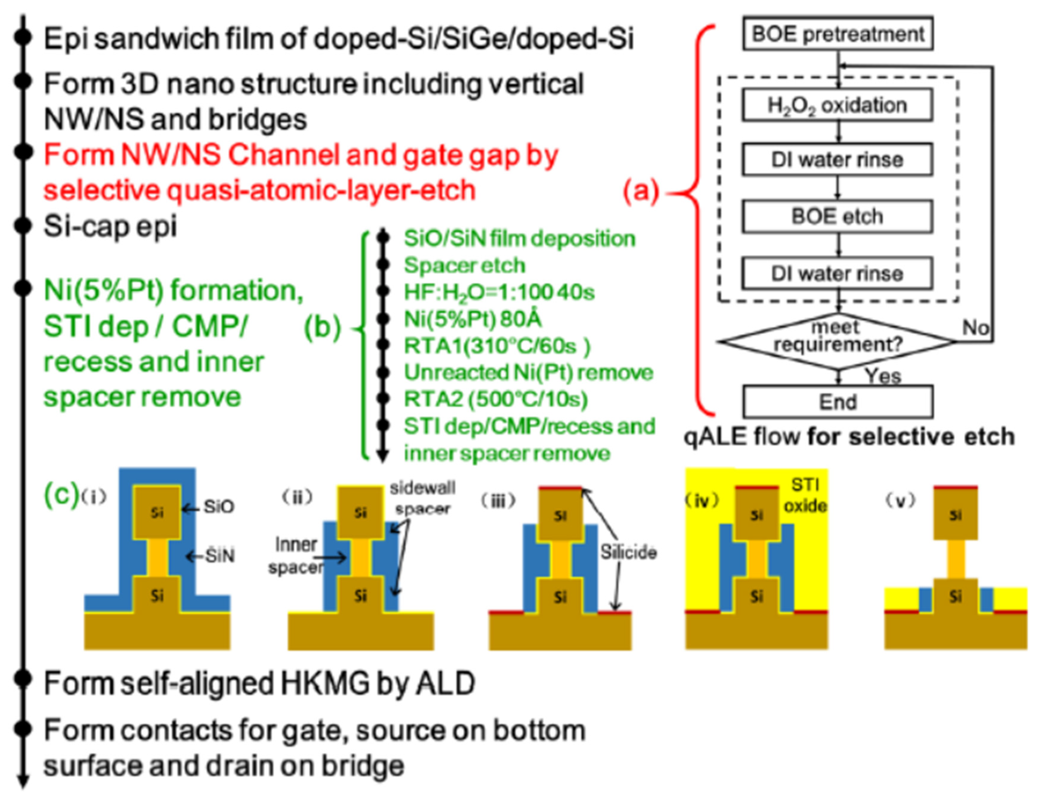
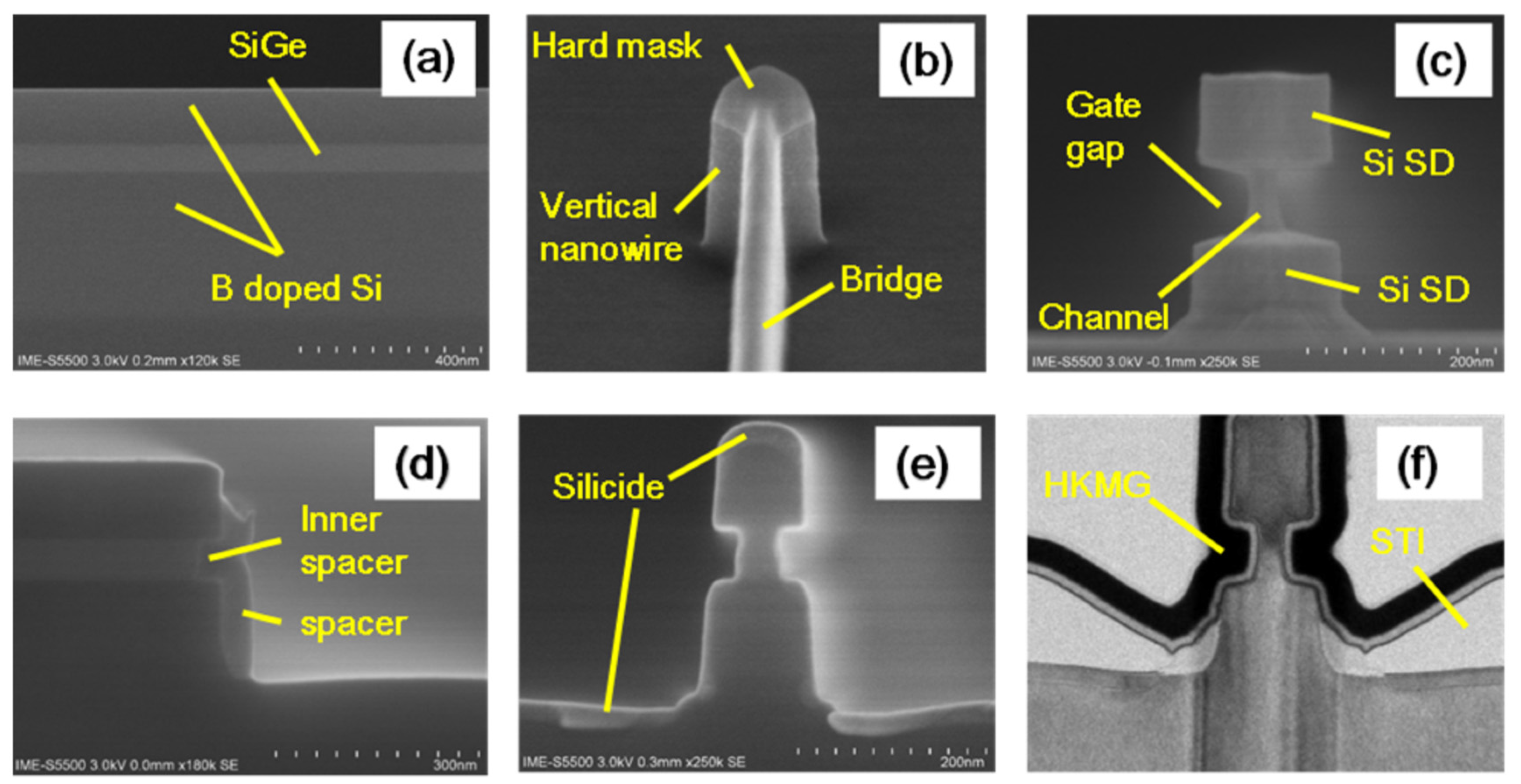
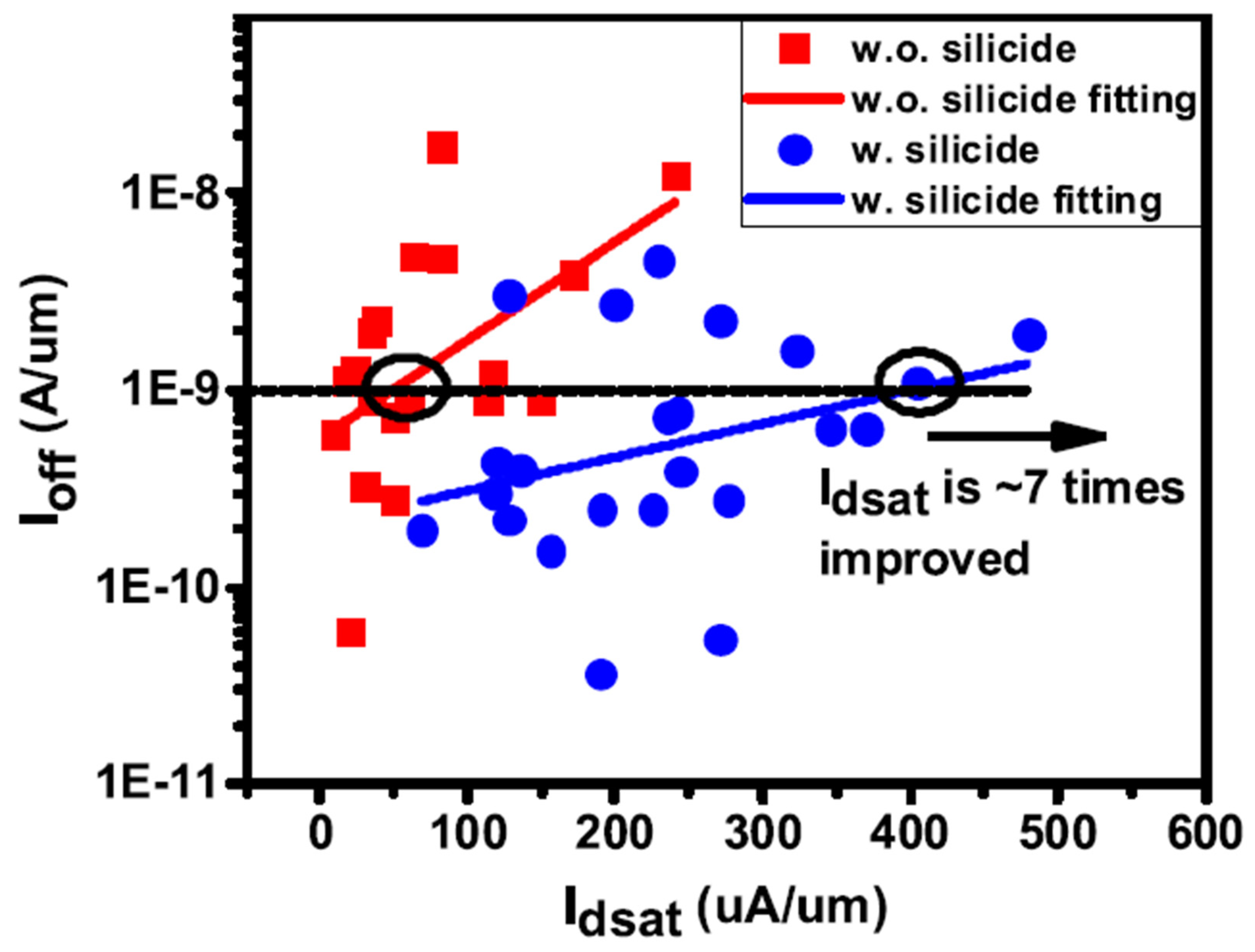
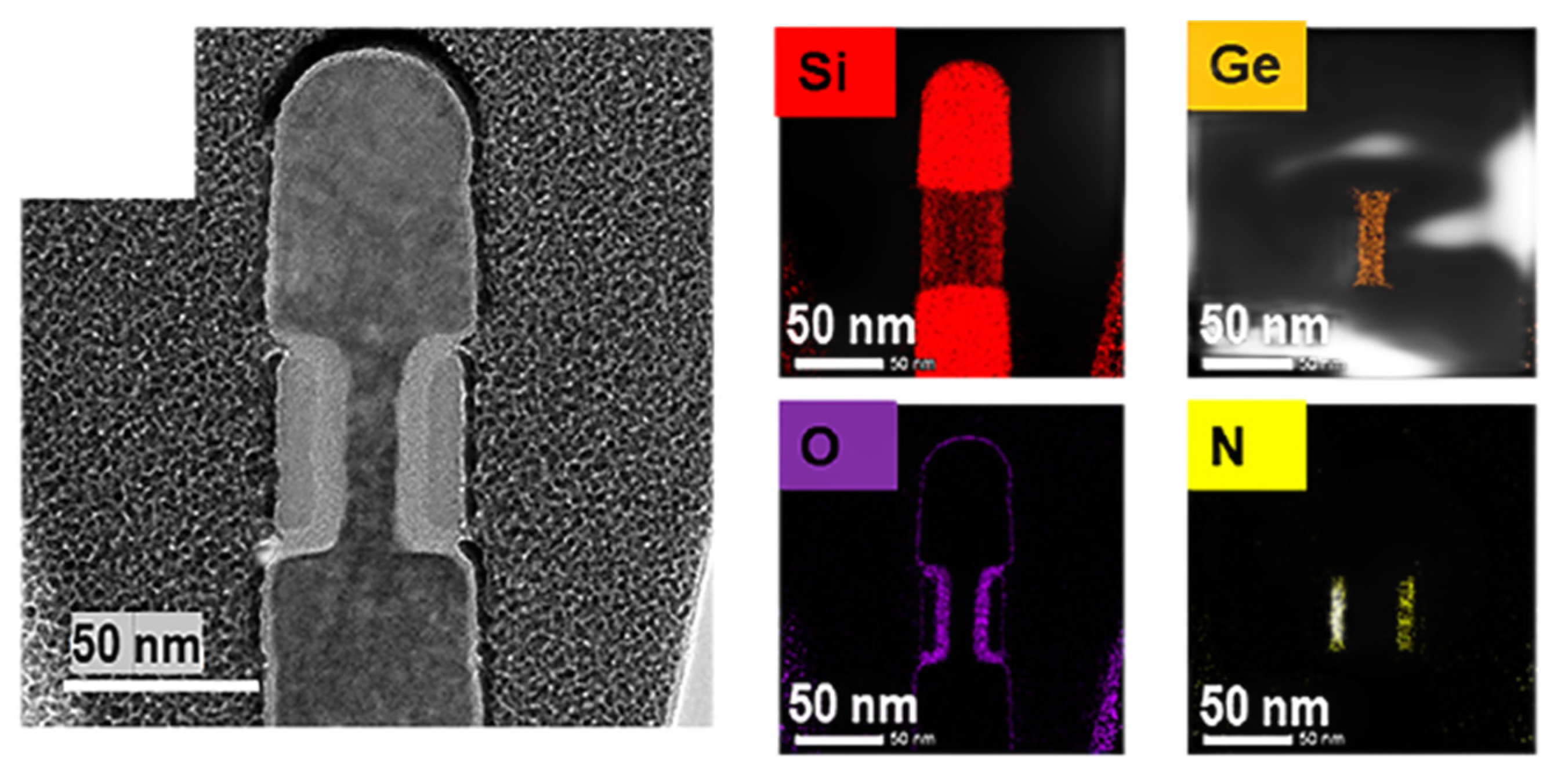
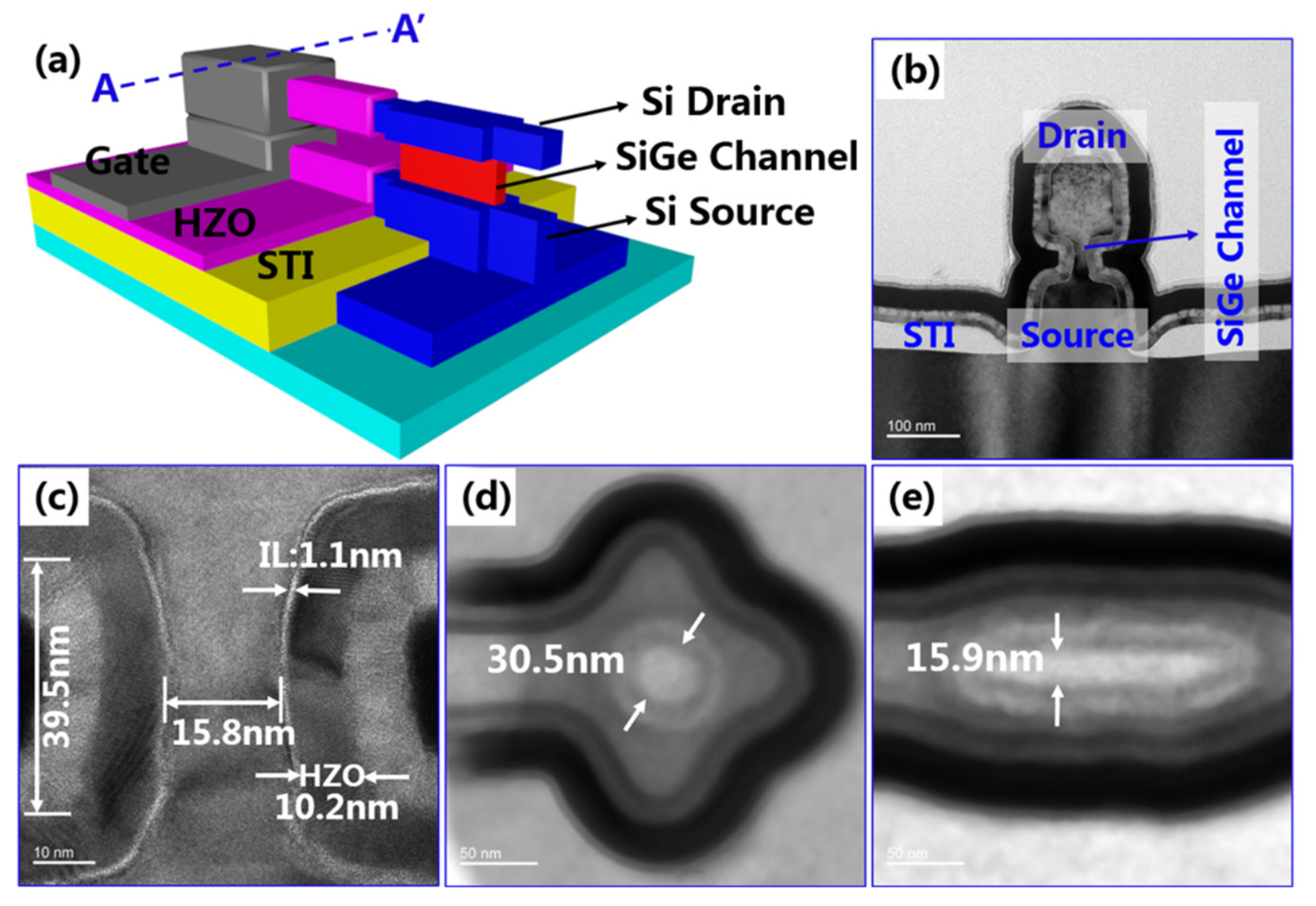
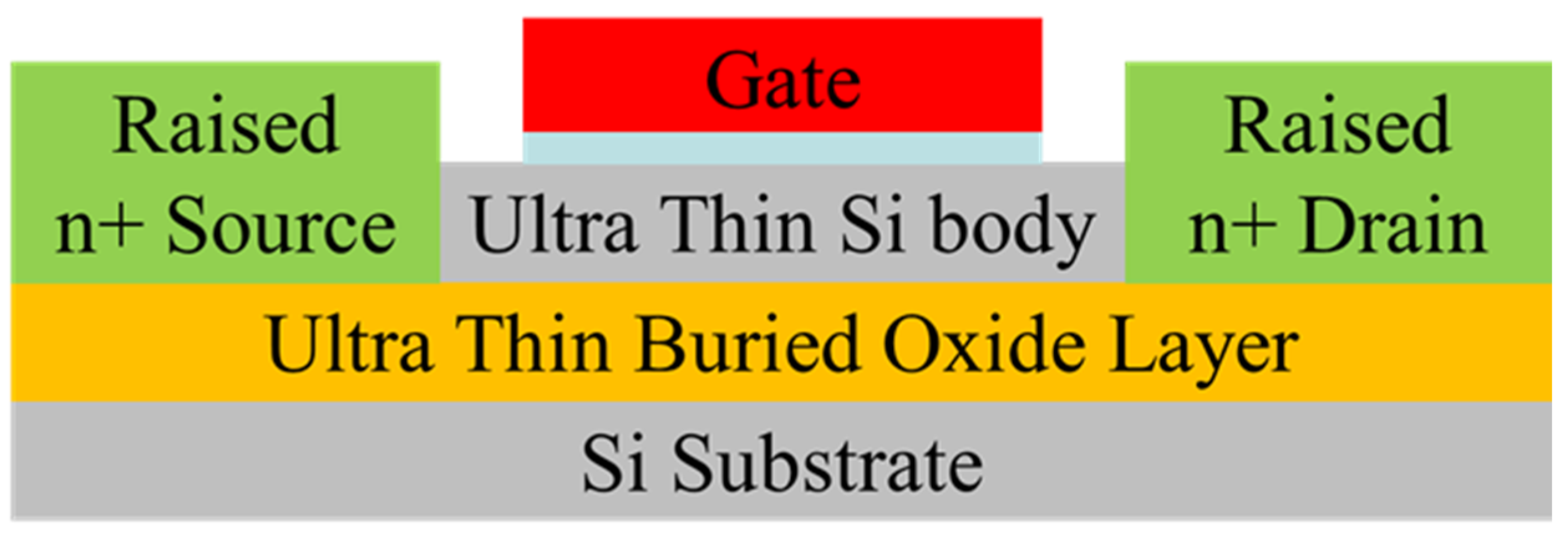
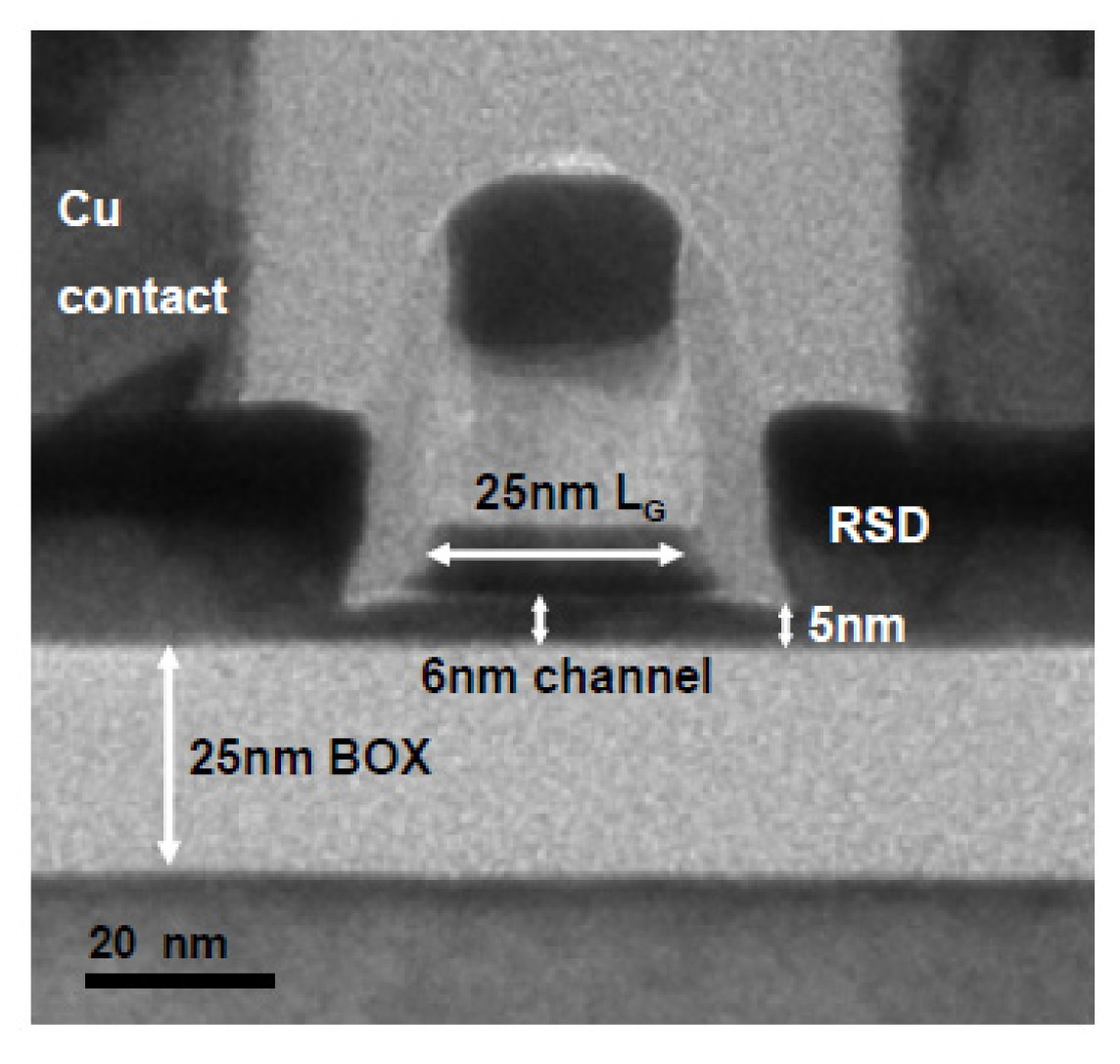

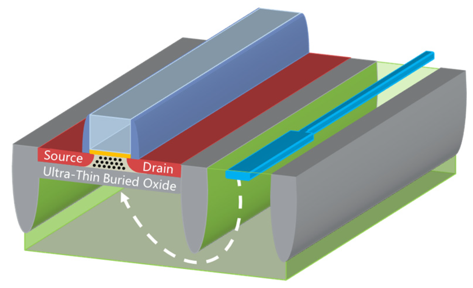
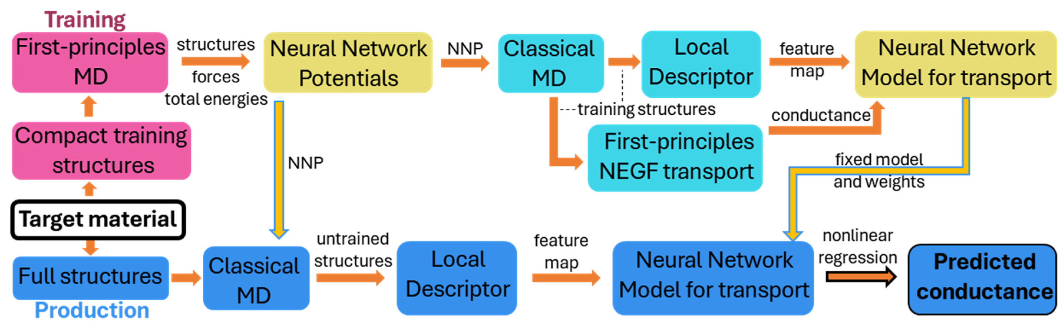
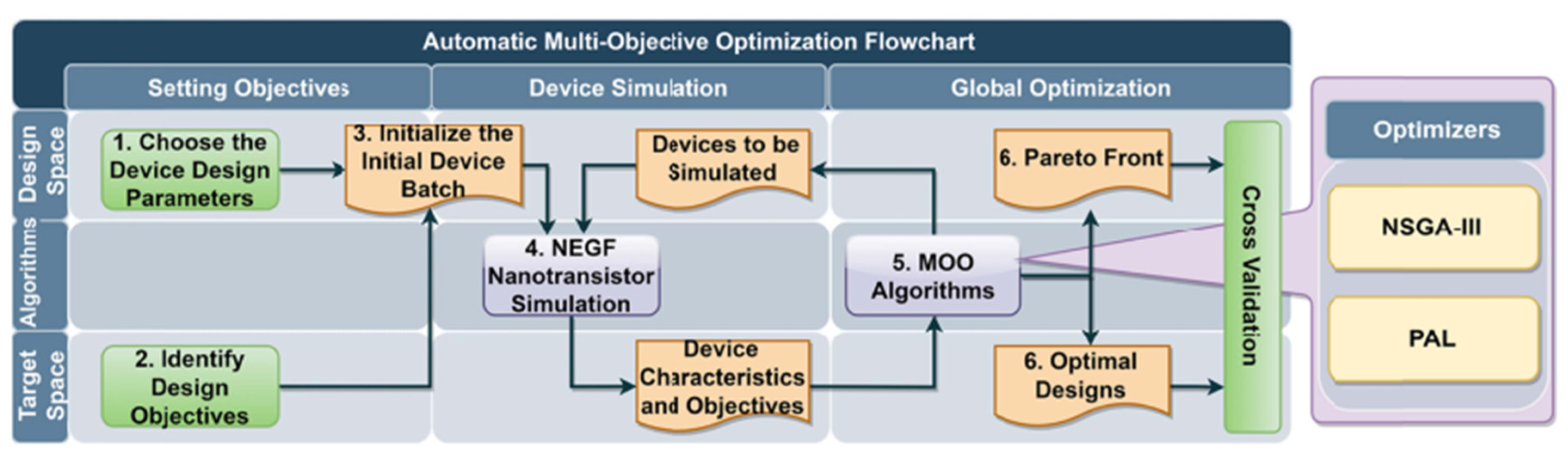
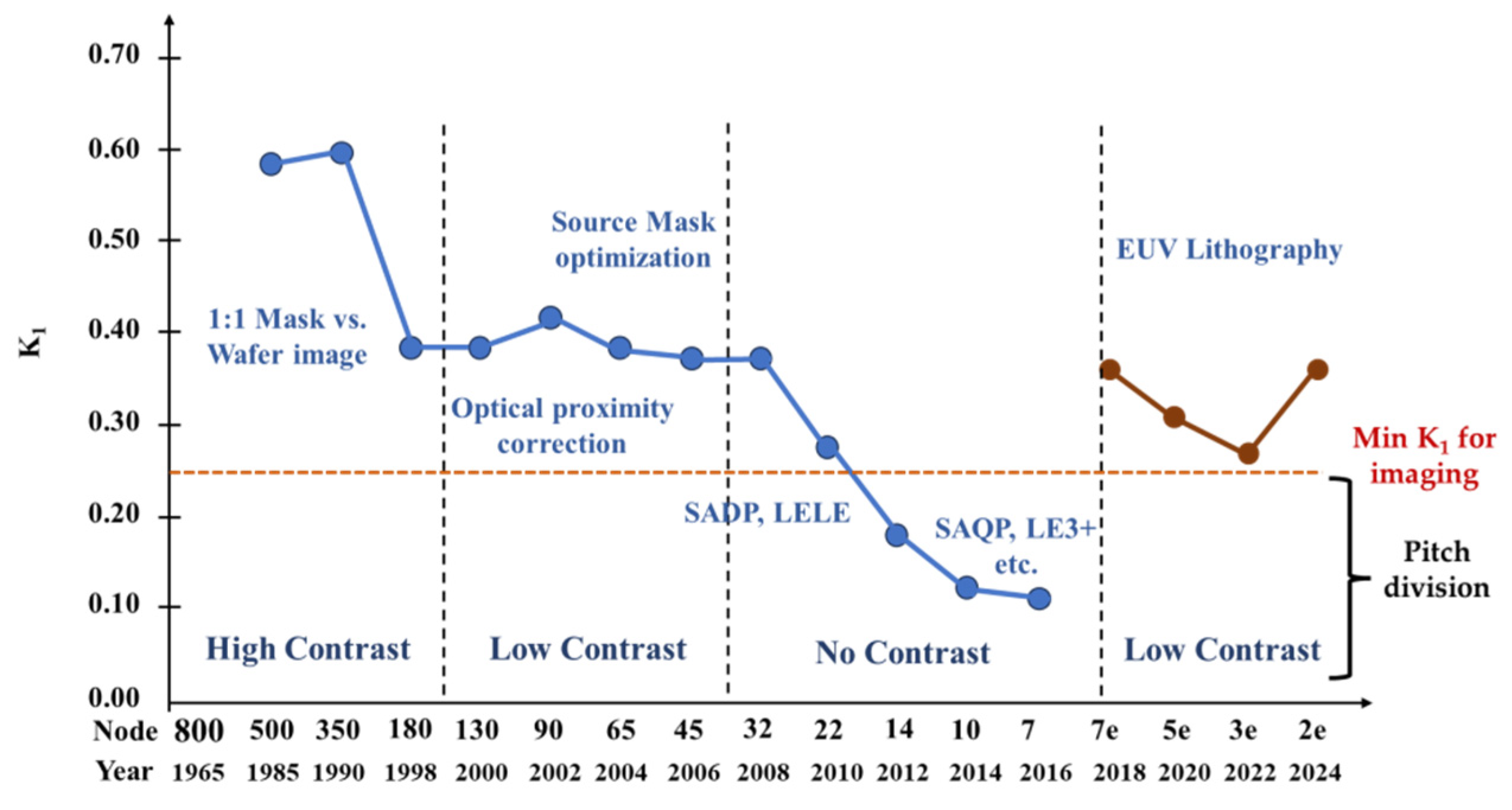

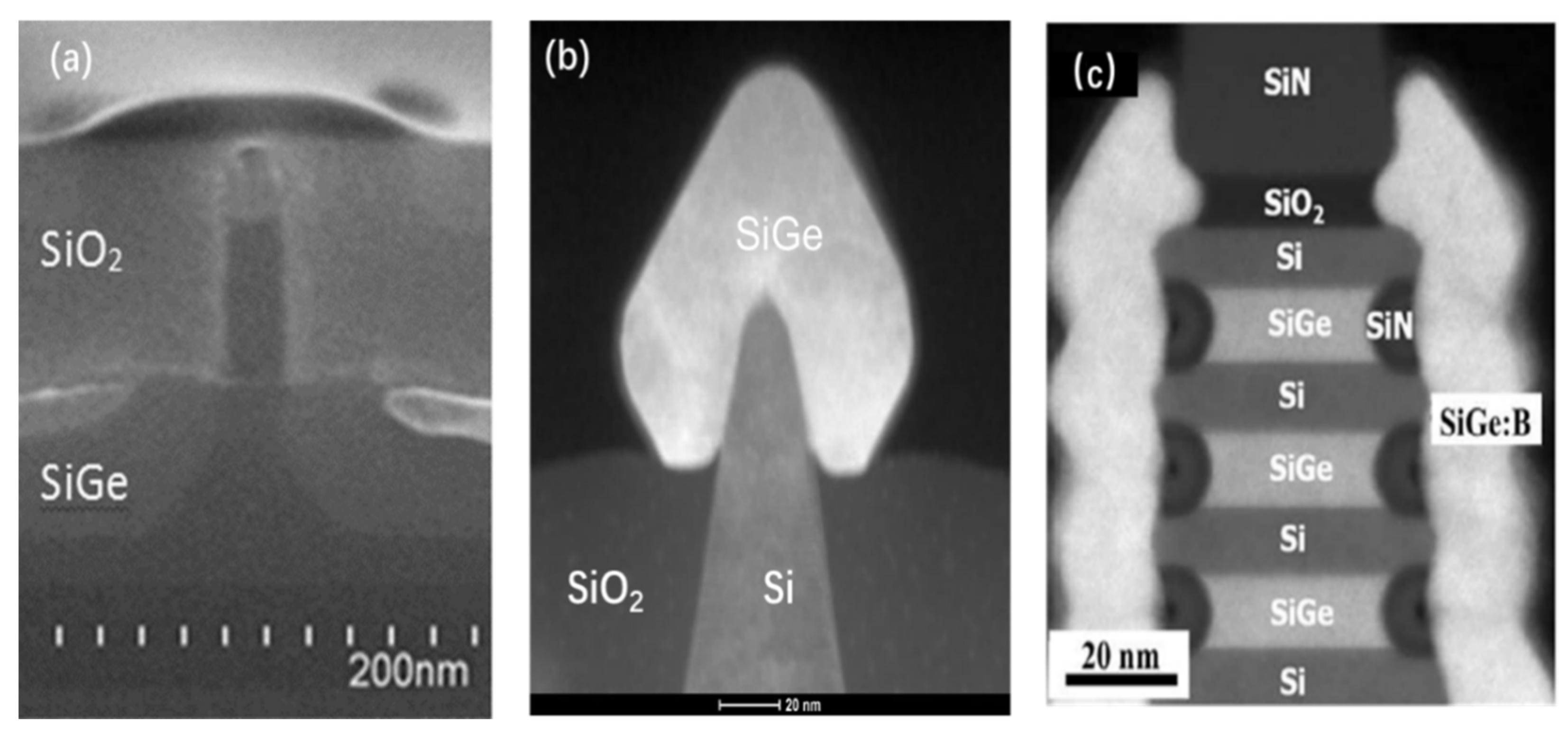
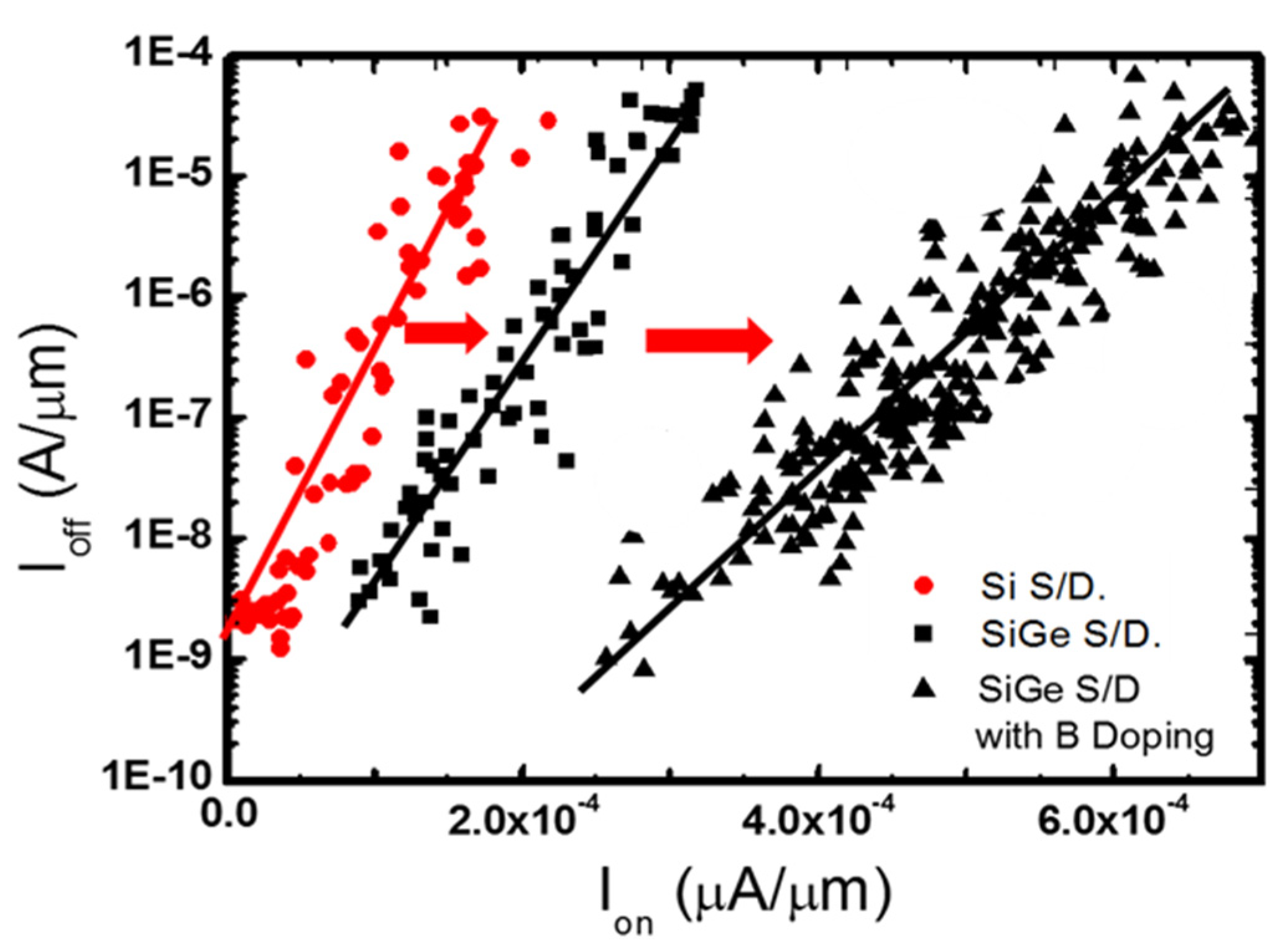
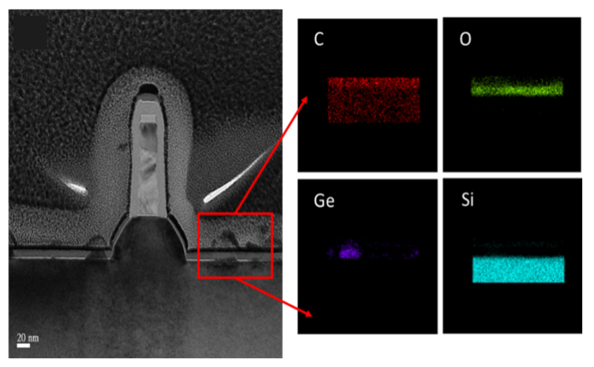
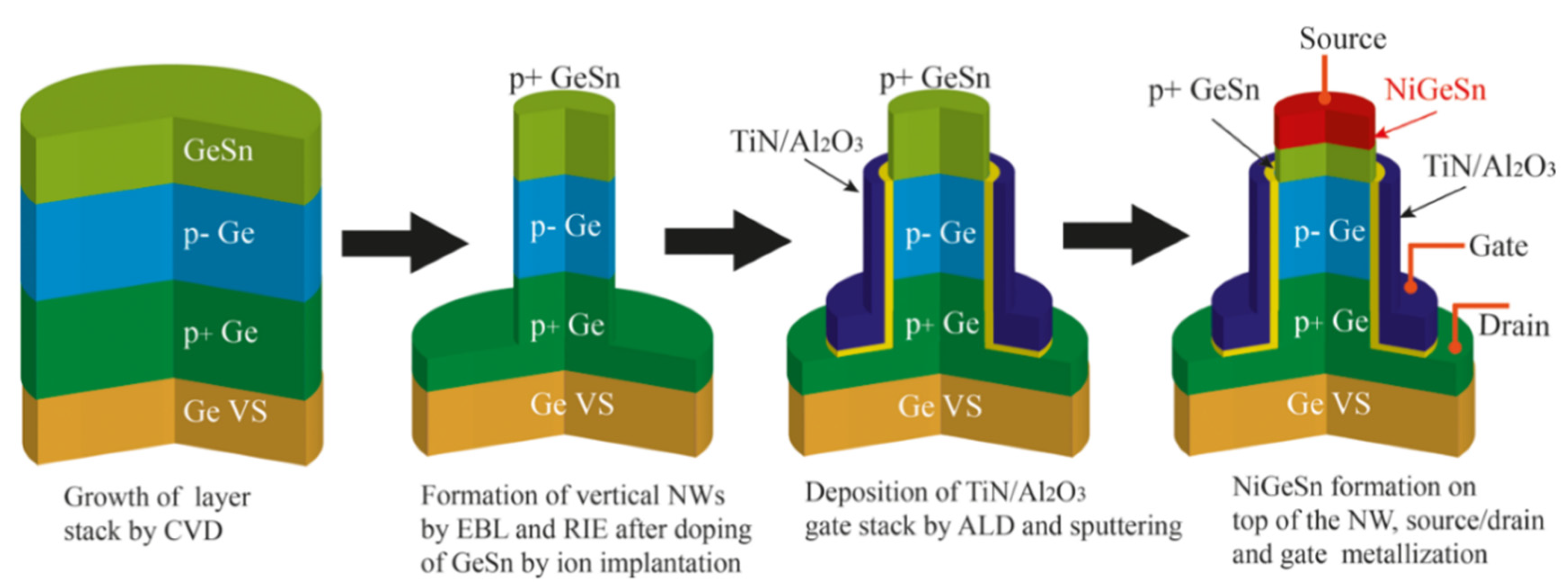

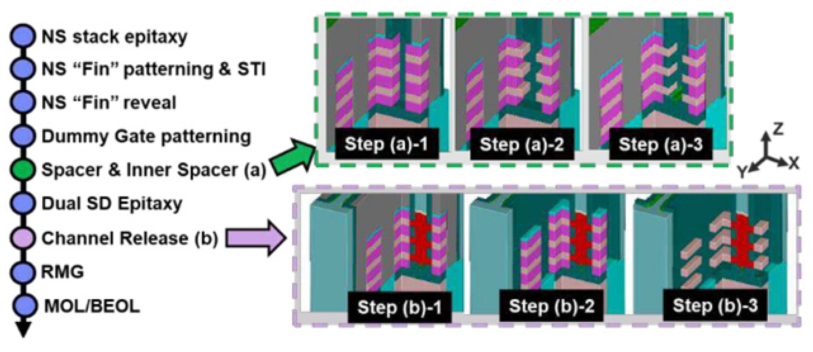
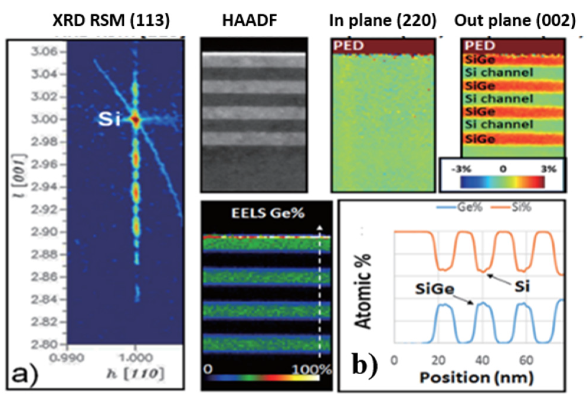
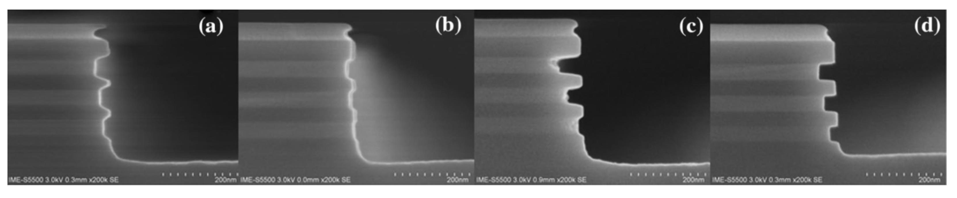
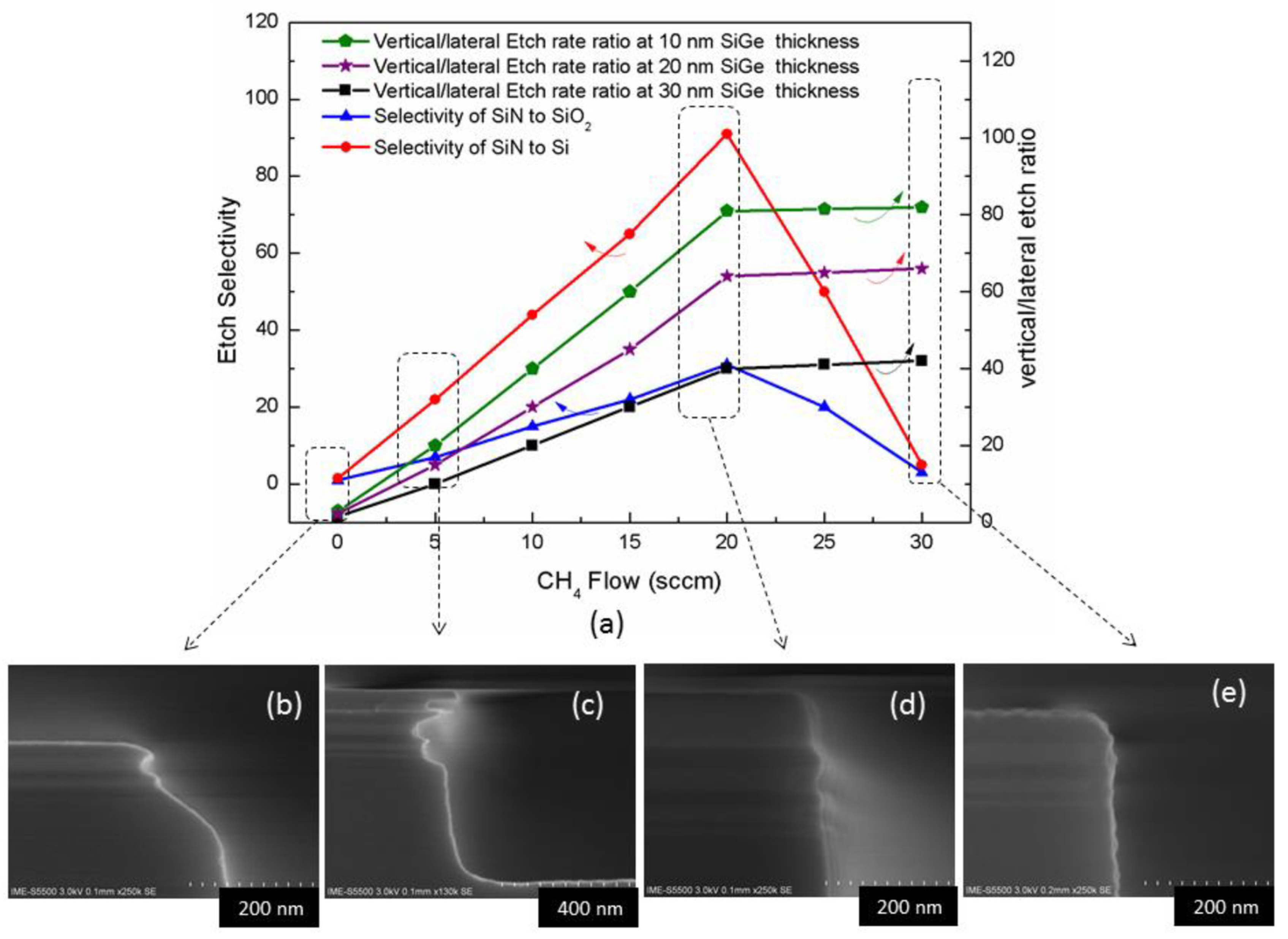

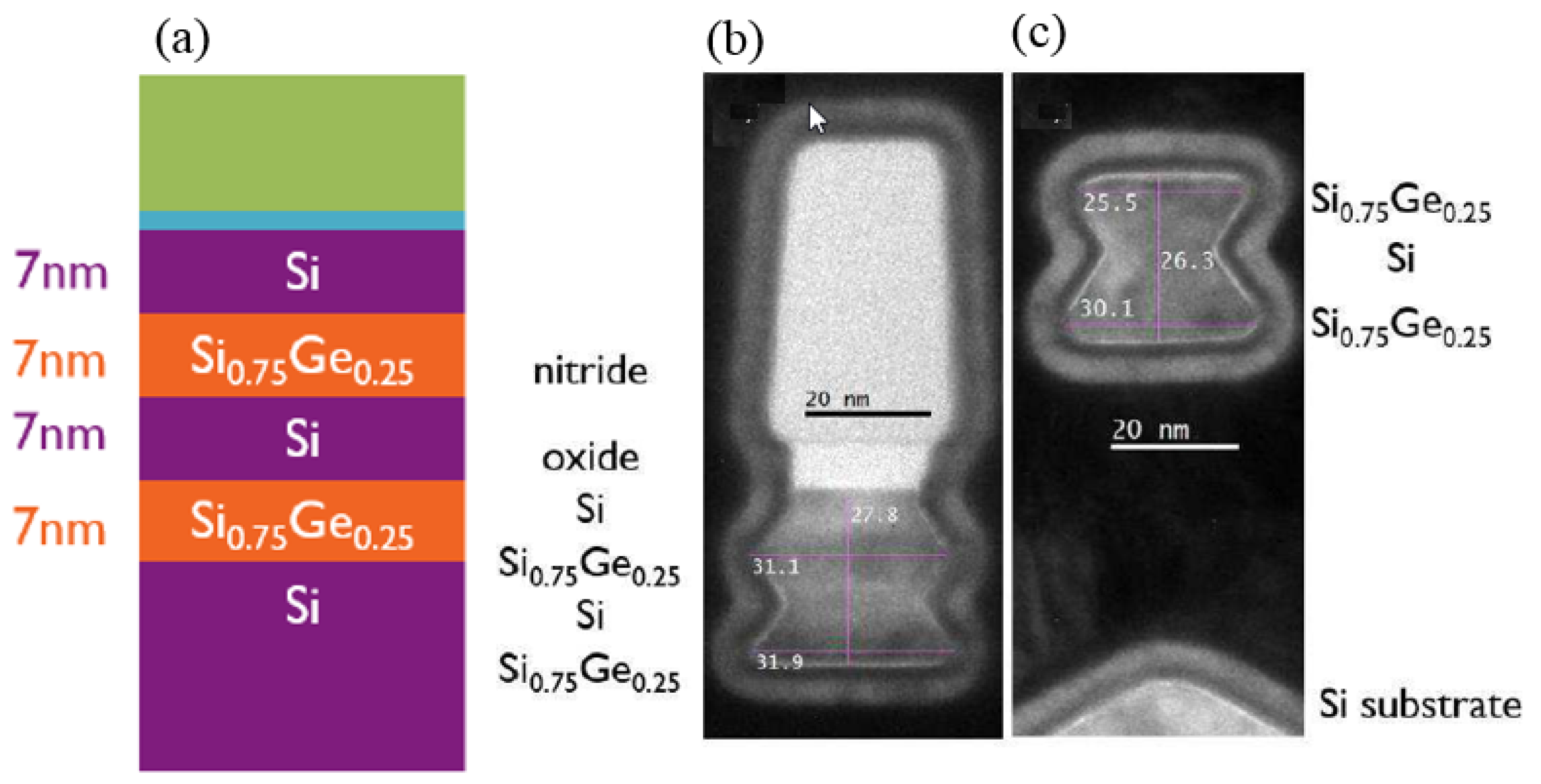
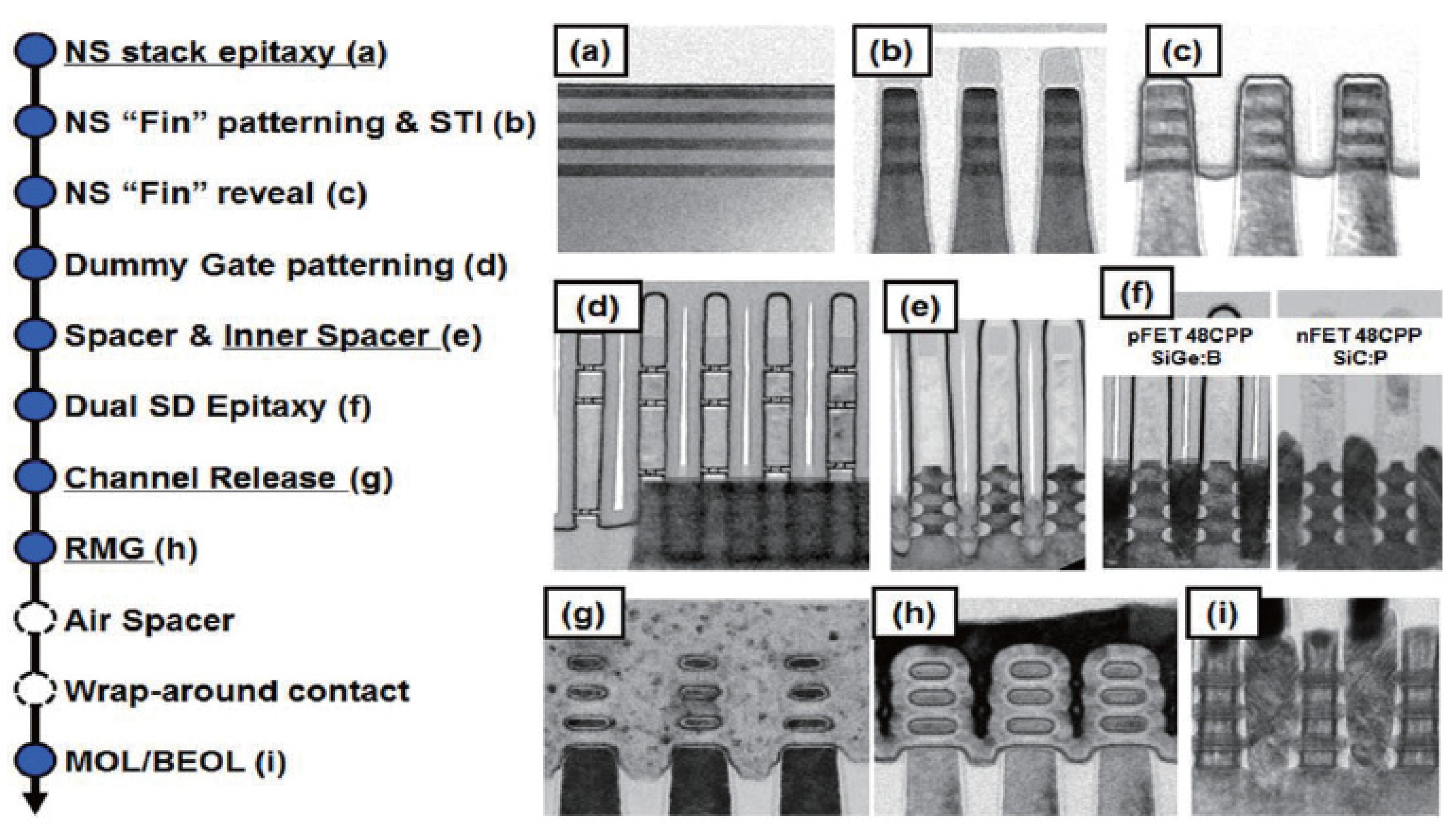
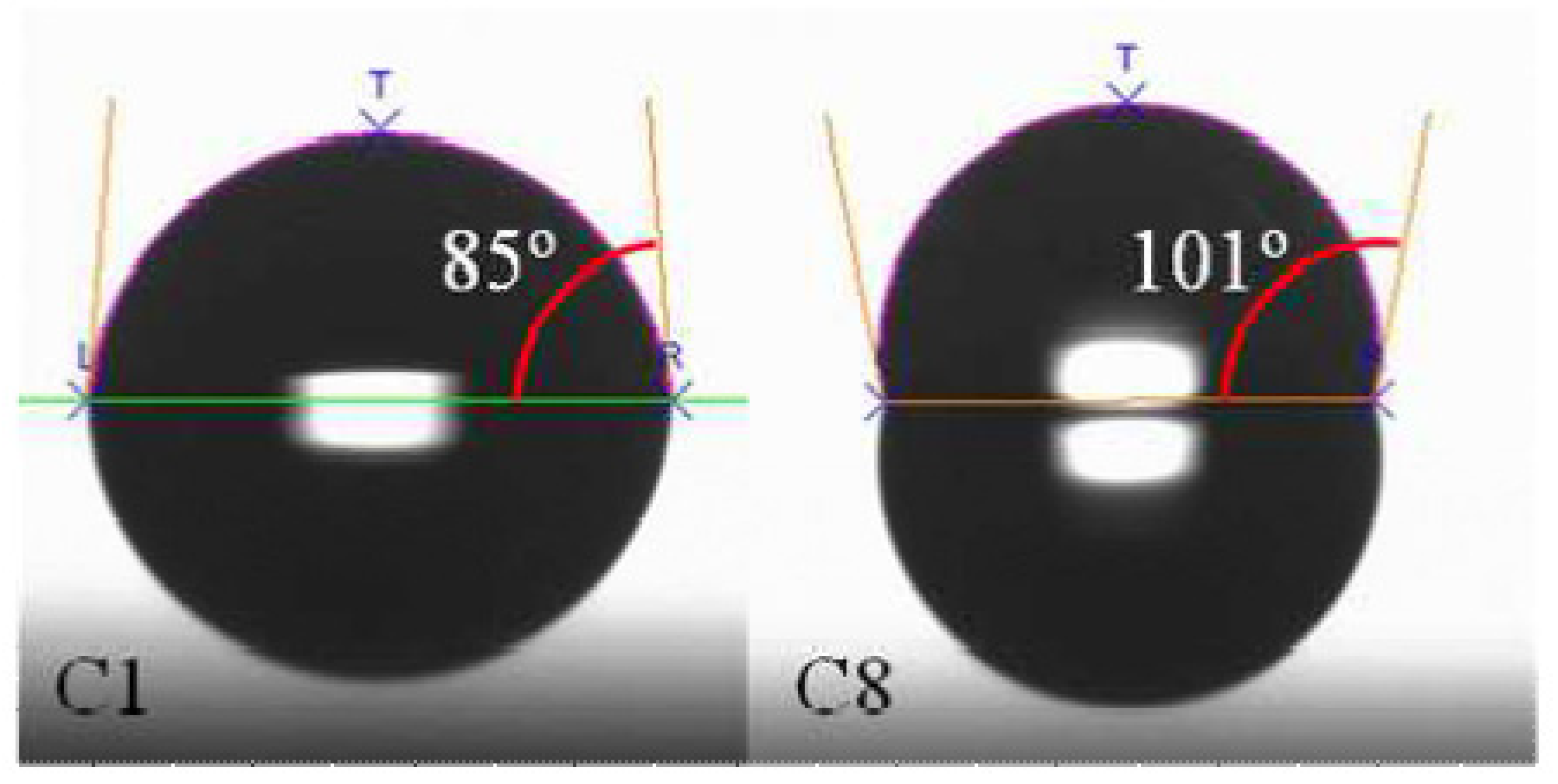

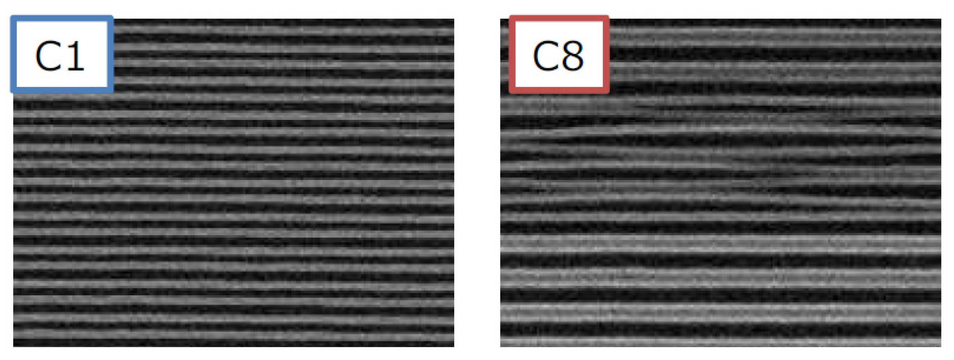
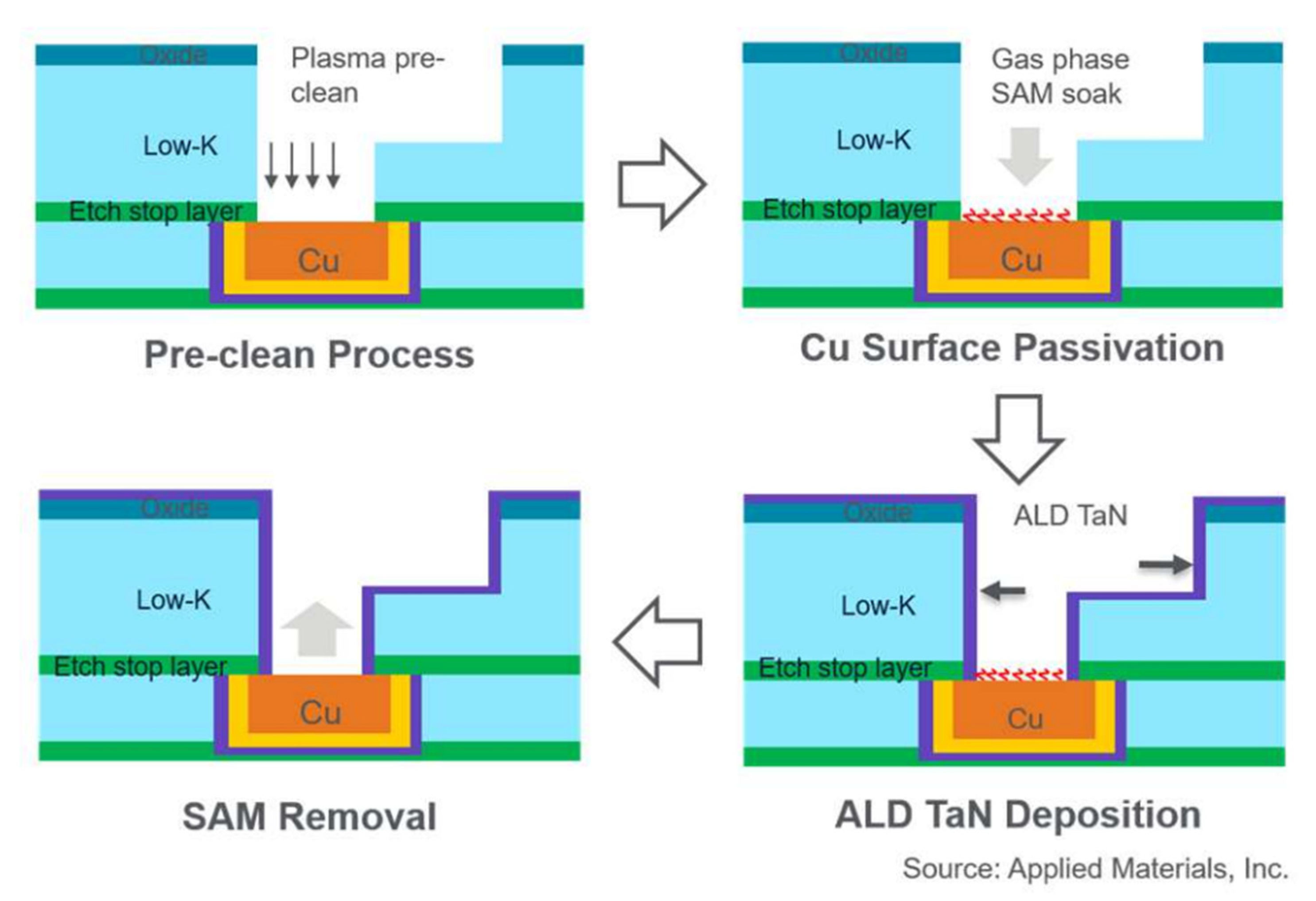
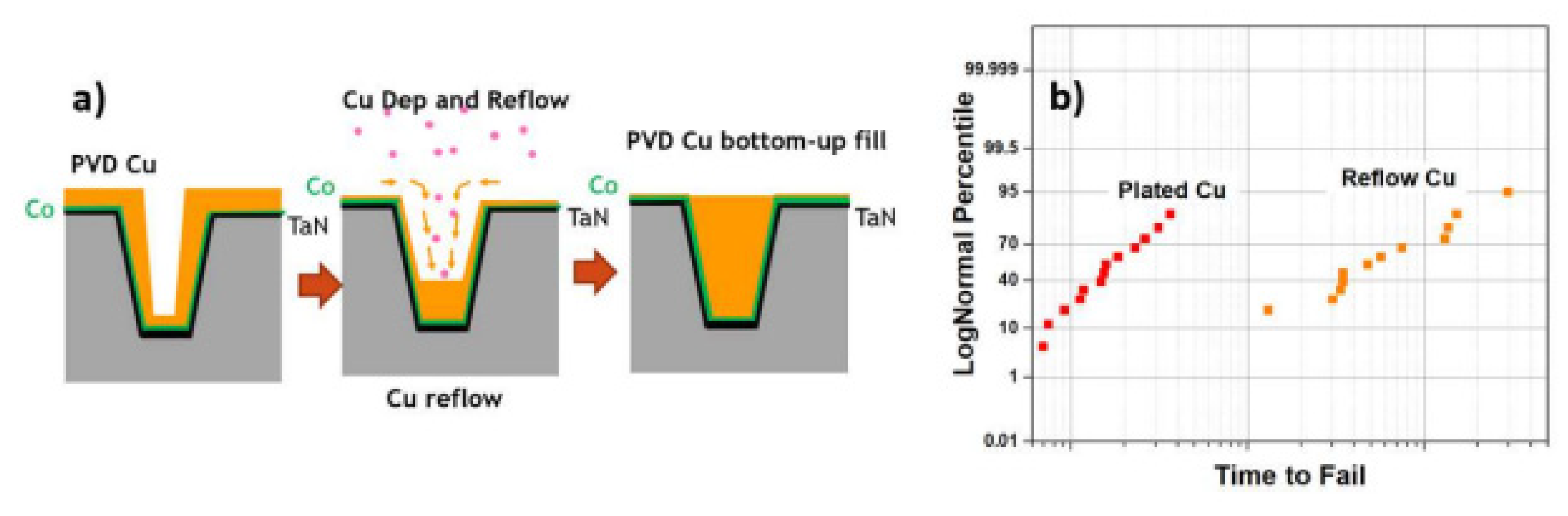
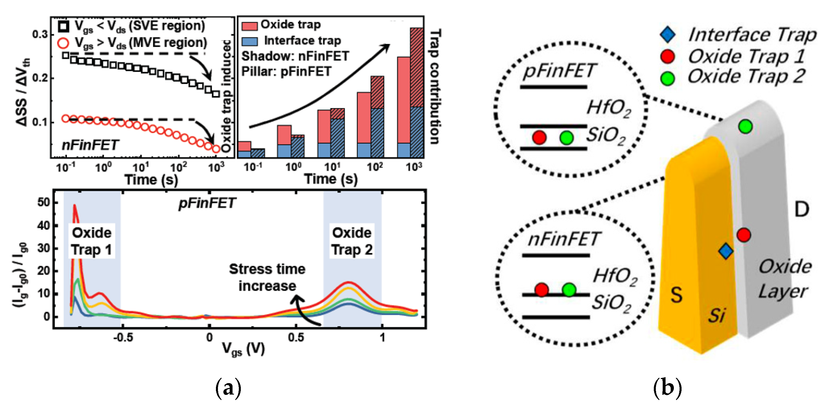
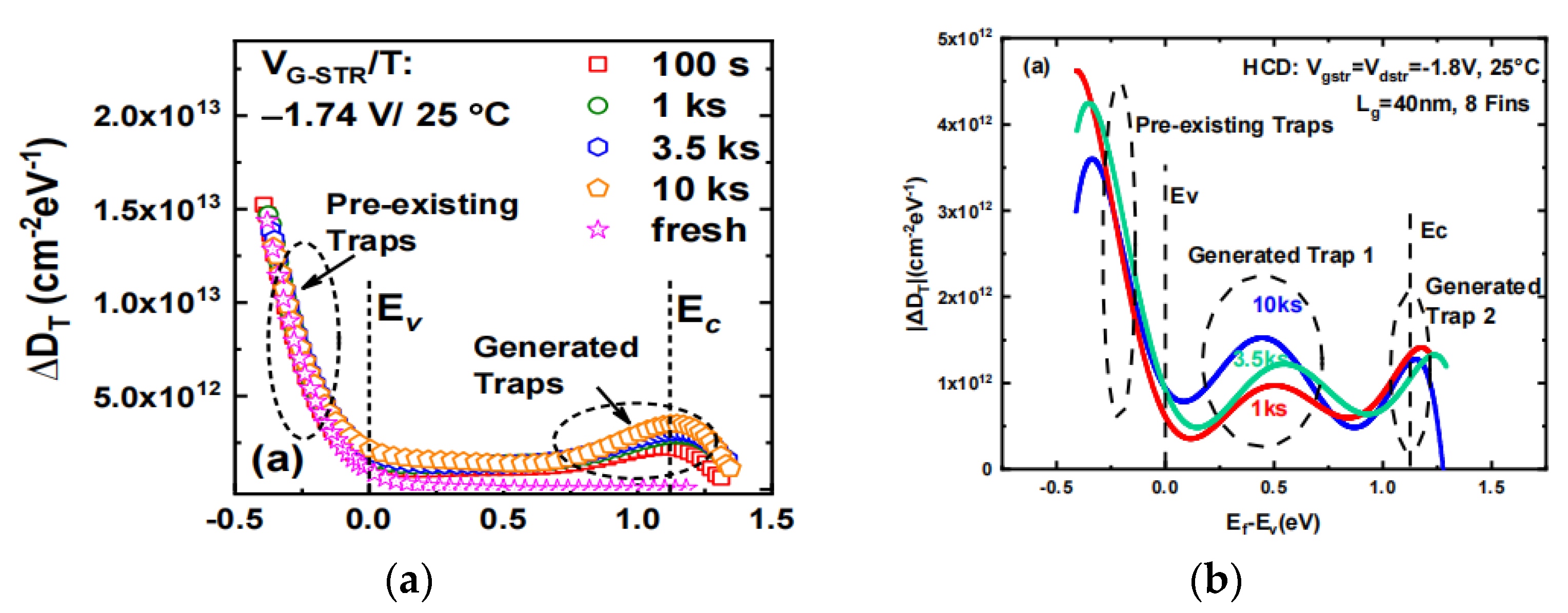
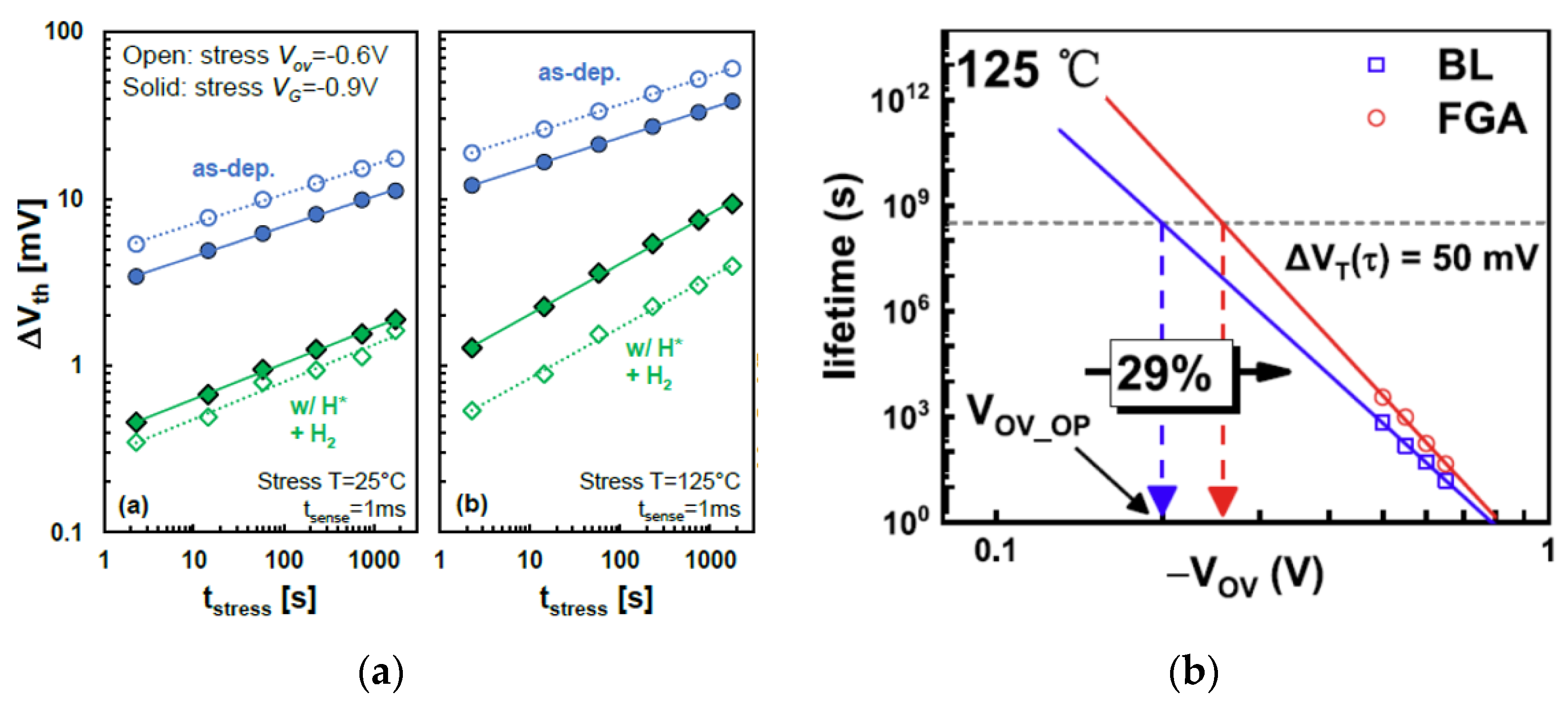
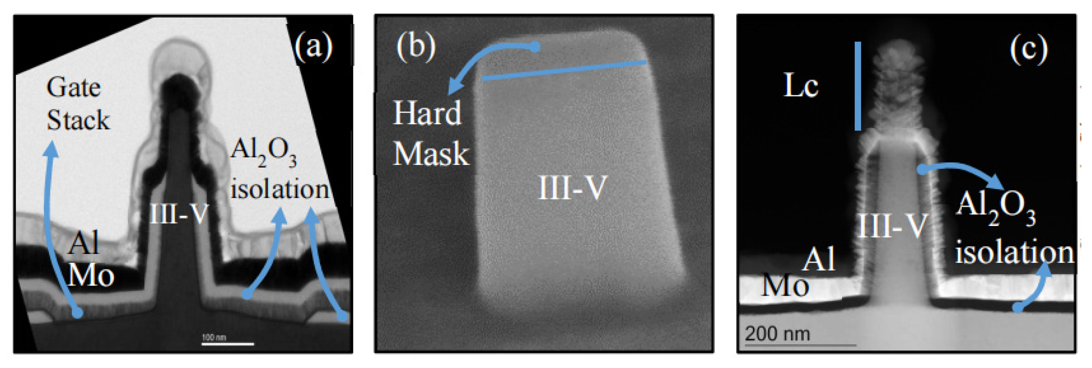
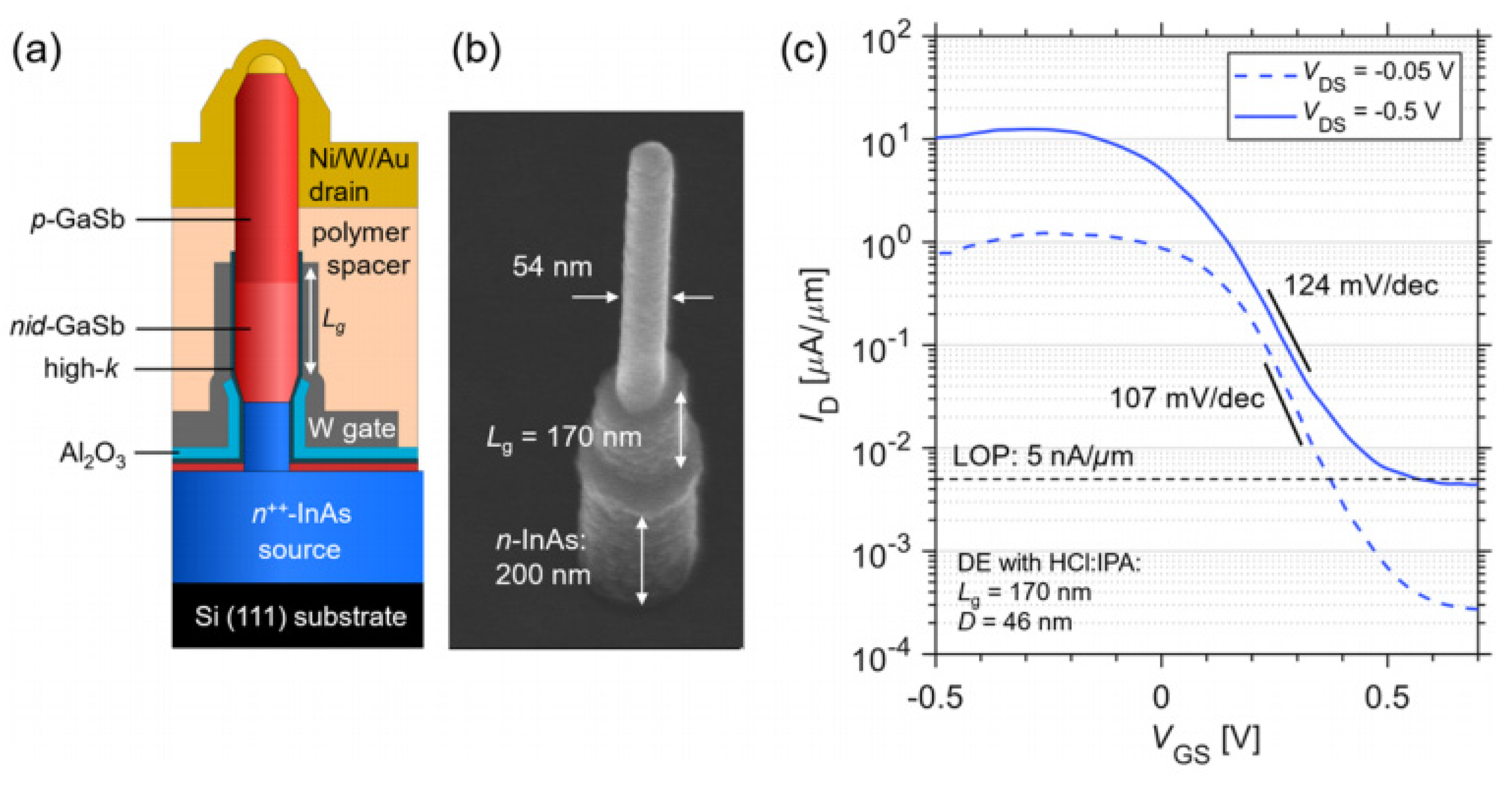
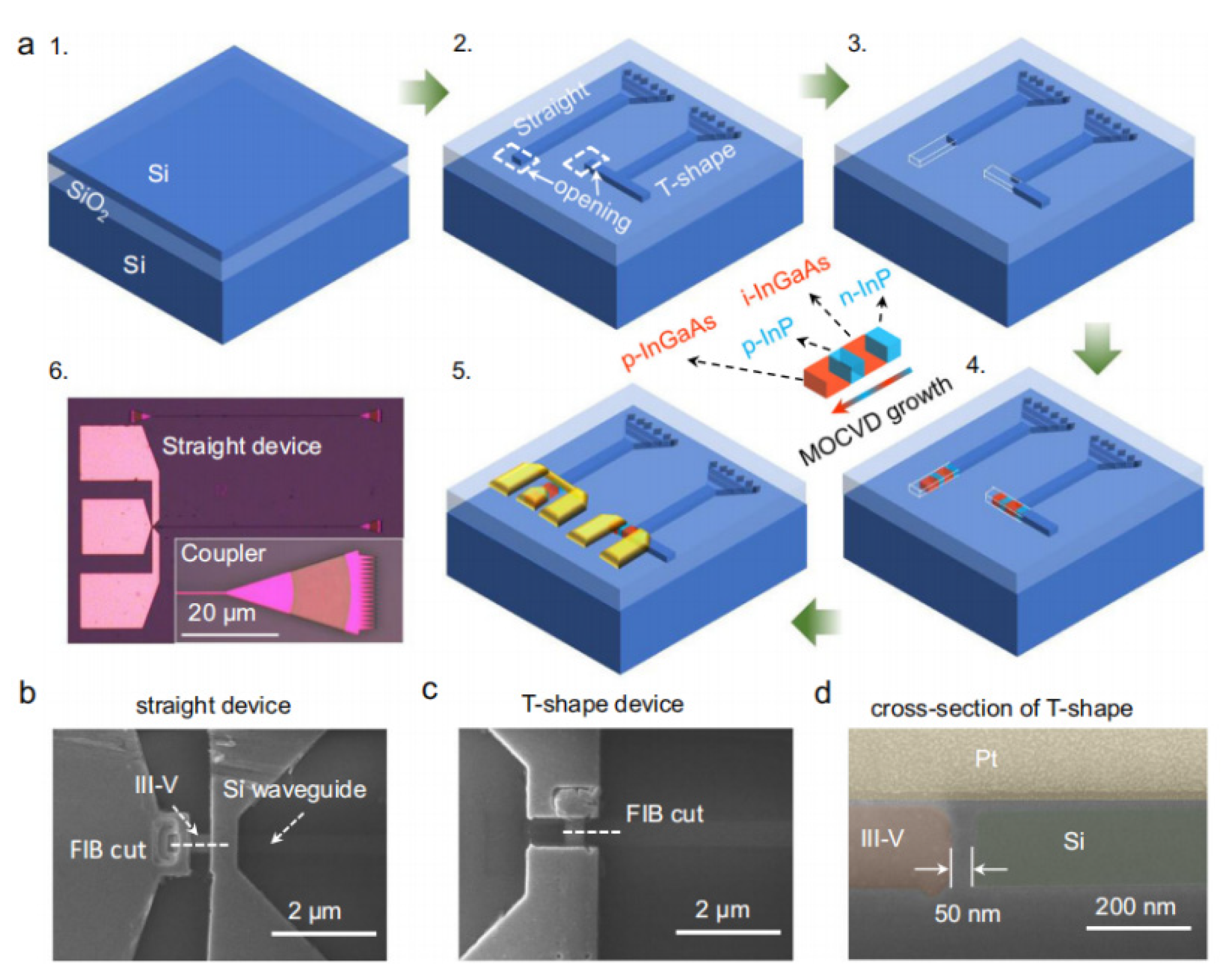
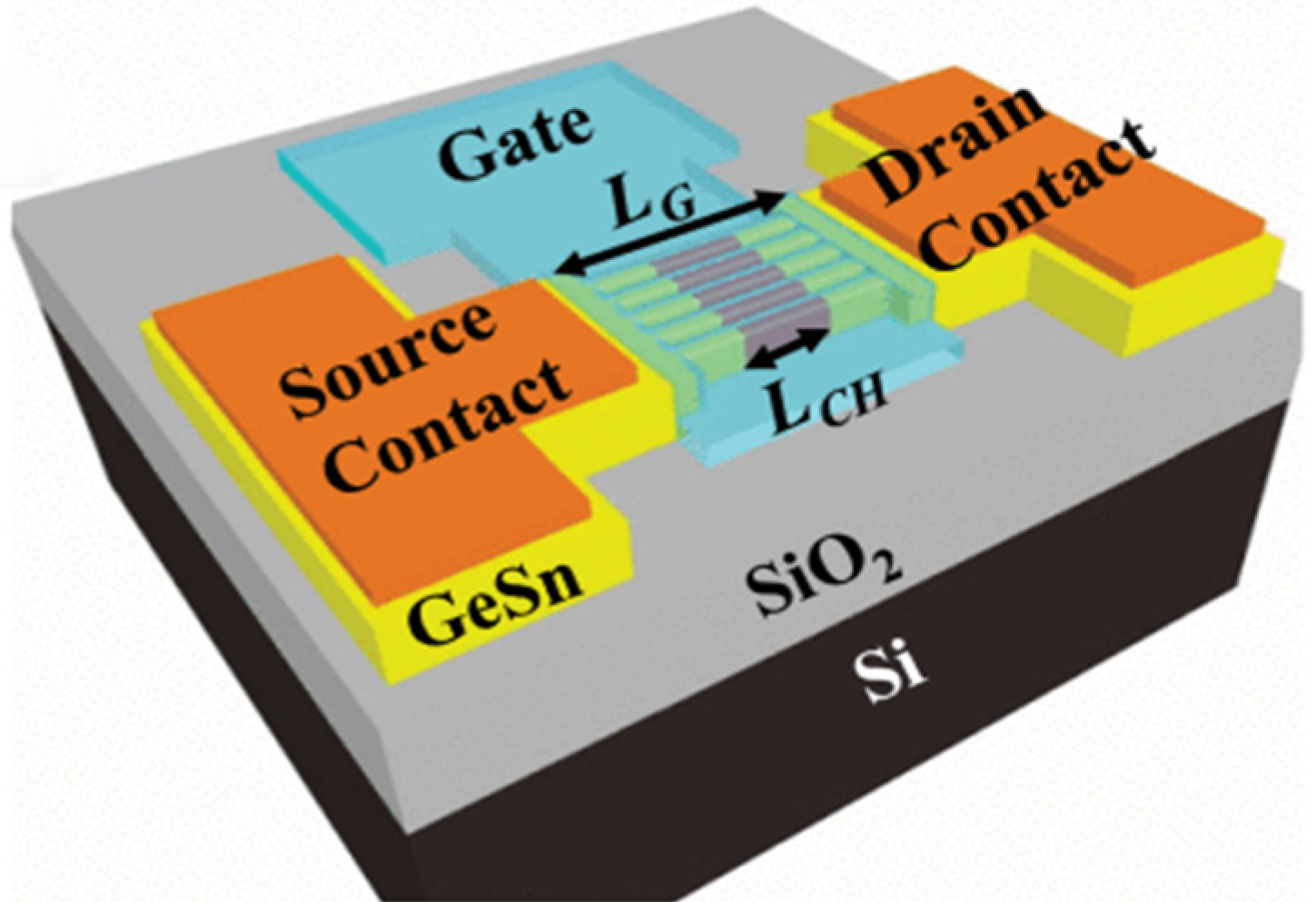

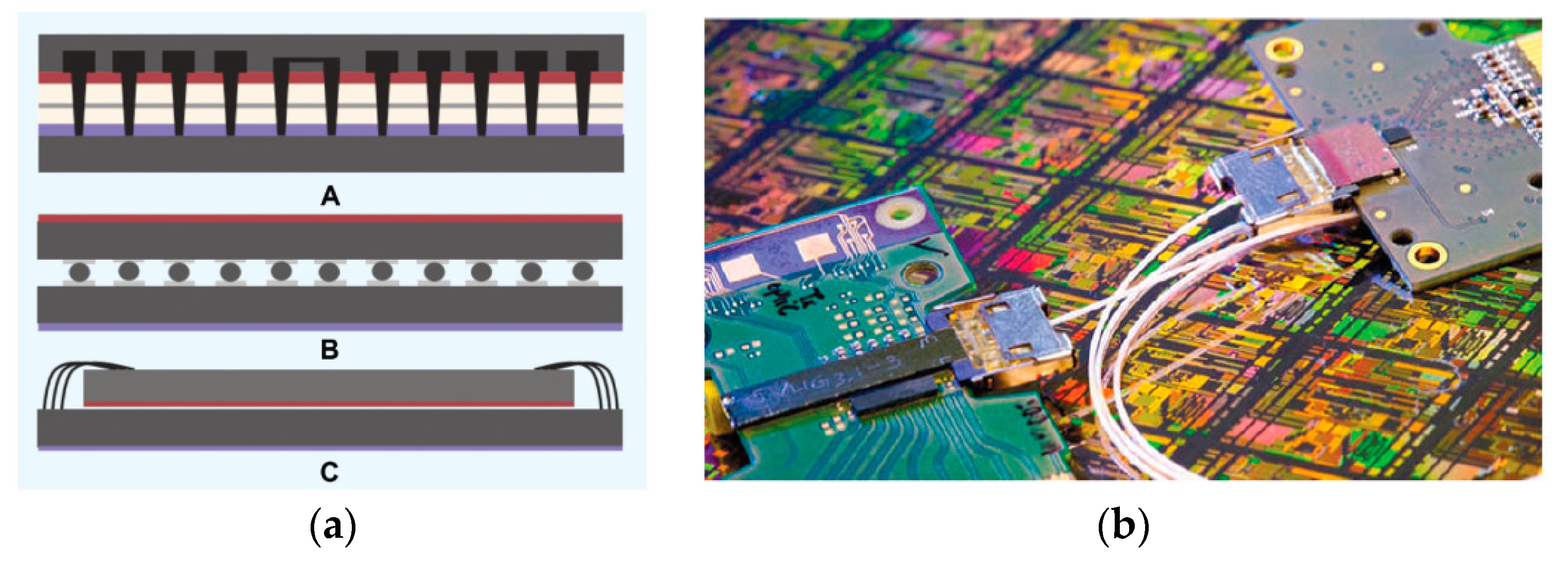
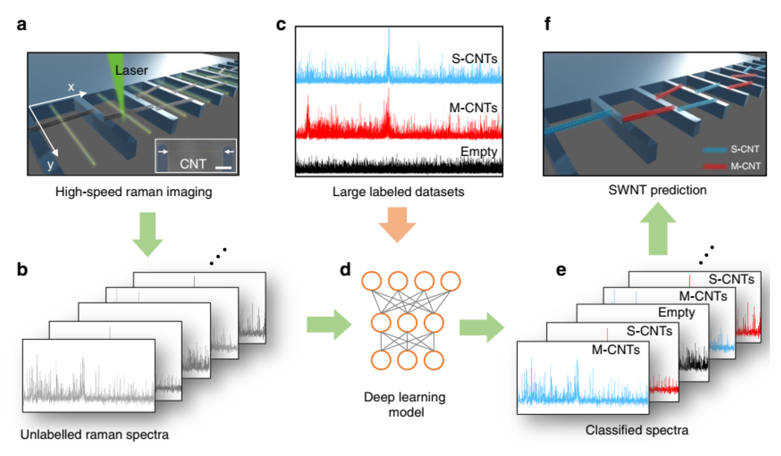

| Year | Ref. | Material System | ION [μA/μm] | ION/IOFF Ratio | SSmin [mV/dec] | <60? |
|---|---|---|---|---|---|---|
| 2007 | [38] | Si | 12.1 | 104 | ~52.8 | √ |
| 2008 | [39] | Si | <0.1 | <107 | 42 | √ |
| 2009 | [40] | Ge/Si | 0.4 | >106 | 35 | √ |
| 2010 | [41] | Si | ~2 | 108 | 46 | √ |
| 2011 | [42] | Si | <10−4 | 104 | 30 | √ |
| 2012 | [43] | Strain-Si | 0.1 | 107 | 76 | × |
| 2012 | [44] | Si | ~0.1 | 106 | 52 | √ |
| 2012 | [45] | Si | 0.15 | ~105 | 36 | √ |
| 2013 | [46] | Ge/Si | 107 | 49 | √ | |
| 2014 | [47] | Si | 39 | >105 | 69 | |
| 2014 | [48] | Si | 20 | 108 | 29 | √ |
| 2015 | [49] | Ge/strain-SOI | <1 | 107 | 29 | √ |
| 2016 | [50] | Si | <0.01 | 105 | 34 | √ |
| 2017 | [51] | Si | 2.0 | 108 | 75 | × |
| 2017 | [52] | Ge/Si | 14 | 107 | >200 | × |
| 2019 | [53] | Si | <0.01 | 104 | 17 | √ |
| 2020 | [54] | Si | 40 | ~108 | 69 | × |
| 2020 | [23] | SiGe | <0.01 | ~106 | 65.4 | × |
| Year | Ref. | Material System | ION [μA/μm] | ION/IOFF Ratio | SSmin [mV/dec] | <60? |
|---|---|---|---|---|---|---|
| 2011 | [24] | Hetero-InGaAs | 10 | 105 | 55~60 | √ |
| 2012 | [25] | GaAsSb/InGaAs | 135 | 104 | 100 | × |
| 2012 | [26] | InAs/Si | 2.4 | 106 | 150 | × |
| 2012 | [27] | InAs/GaSb | 180 | 104 | 200 | × |
| 2012 | [28] | InAs/Si | <1 | ~106 | 21 | √ |
| 2013 | [29] | InGaAs/GaAsSb | 740 | 102 | NA | × |
| 2015 | [30] | InGaAs | 1 | 106 | 64 | × |
| 2015 | [31] | InGaAs/GaAsSb | 84 | <105 | 64 | × |
| 2015 | [32] | GaAsSb/InGaAs | 275 | 105 | 55 | √ |
| 2016 | [33] | InAs/Si | 4 | 70 | × | |
| 2017 | [34] | Ge/GeSn | 2.4 | 104 | 215 | × |
| 2018 | [35] | InGaAsSb/InAs | <10 | <105 | 75 | × |
| 2018 | [36] | InGaAsSb/InAs | <0.1 | <104 | 35 | √ |
| 2019 | [37] | GaSb/InAs | <104 | 40 | √ | |
| 2021 | [22] | InGaAs/GaAsSb | <0.1 | ~103 | 42 | √ |
| Year | Institution | Sn | Channel Length | IOFF (μA/μm) | ION/IOFF Ratio | SS (mV/dec) | Stacks | Ref. |
|---|---|---|---|---|---|---|---|---|
| 2017 | National Taiwan University | 6% | 150 nm | 1400 | —— | 84 | 1–2 | [189] |
| 10% | 60 nm | 1850 | —— | |||||
| 2019 | National Taiwan University | 9% | —— | 120 | —— | 84 | 3 | [190] |
| 2020 | PGI 9 | 8% | 150 nm | —— | 3 × 10⁶ | 72 | 1 | [191] |
| 2020 | PGI 9 | 8% | —— | —— | 3 × 10⁶ | 67 | 1 | [192] |
| 2021 | National Taiwan University | 10% | 80 nm | 86 | —— | —— | 4 | [193] |
| Year | Sn Composition | GeSn Growth | Bonding Type | Strain | Direction of Wafer | Ref. |
|---|---|---|---|---|---|---|
| 2012 | 0–3% | vacuum evaporation system | Seed epitaxy | 3% | <100> | [346] |
| 2017 | 8% | CVD | DWB | −0.9% | [349] | |
| 2018 | 8% | MBE | Epitaxy | −0.9% | <111> | [353] |
| 2020 | 5.4% | 1.4% | [355] | |||
| 2022 | 7% | RP-CVD | fusion bonding | −0.32–0.47% | <100> | [357] |
| Year | Transistor Type | Gate Length/nm | Fin Width/nm | Subthreshold Slope/mV/Decade | ION/IOFF Ratio | Ref. |
|---|---|---|---|---|---|---|
| 2017 | p-FinFET | 50 | 20 | <90 | >104 | [350] |
| 2018 | p-FinFET | 4 µm | 40 | 139 | [368] | |
| 2018 | p-FinFET | 200 | 30 | 79 | >104 | [354] |
| 2018 | p-FinFET | 50 | 5 | 63 | 104 | [369] |
| 2018 | p-FinFET | 100 | 15 | 93 | >104 | [354] |
| 2019 | p-GAAFET | 60 | 15 | 74 | [371] | |
| 2019 | p-FinFET | 80 | 40 | 114 | 104 | [372] |
| 2021 | p-GAAFET | 60 | 3 | 66 | 1.2 × 10⁶ | [373] |
Disclaimer/Publisher’s Note: The statements, opinions and data contained in all publications are solely those of the individual author(s) and contributor(s) and not of MDPI and/or the editor(s). MDPI and/or the editor(s) disclaim responsibility for any injury to people or property resulting from any ideas, methods, instructions or products referred to in the content. |
© 2024 by the authors. Licensee MDPI, Basel, Switzerland. This article is an open access article distributed under the terms and conditions of the Creative Commons Attribution (CC BY) license (https://creativecommons.org/licenses/by/4.0/).
Share and Cite
Radamson, H.H.; Miao, Y.; Zhou, Z.; Wu, Z.; Kong, Z.; Gao, J.; Yang, H.; Ren, Y.; Zhang, Y.; Shi, J.; et al. CMOS Scaling for the 5 nm Node and Beyond: Device, Process and Technology. Nanomaterials 2024, 14, 837. https://doi.org/10.3390/nano14100837
Radamson HH, Miao Y, Zhou Z, Wu Z, Kong Z, Gao J, Yang H, Ren Y, Zhang Y, Shi J, et al. CMOS Scaling for the 5 nm Node and Beyond: Device, Process and Technology. Nanomaterials. 2024; 14(10):837. https://doi.org/10.3390/nano14100837
Chicago/Turabian StyleRadamson, Henry H., Yuanhao Miao, Ziwei Zhou, Zhenhua Wu, Zhenzhen Kong, Jianfeng Gao, Hong Yang, Yuhui Ren, Yongkui Zhang, Jiangliu Shi, and et al. 2024. "CMOS Scaling for the 5 nm Node and Beyond: Device, Process and Technology" Nanomaterials 14, no. 10: 837. https://doi.org/10.3390/nano14100837
APA StyleRadamson, H. H., Miao, Y., Zhou, Z., Wu, Z., Kong, Z., Gao, J., Yang, H., Ren, Y., Zhang, Y., Shi, J., Xiang, J., Cui, H., Lu, B., Li, J., Liu, J., Lin, H., Xu, H., Li, M., Cao, J., ... Wang, G. (2024). CMOS Scaling for the 5 nm Node and Beyond: Device, Process and Technology. Nanomaterials, 14(10), 837. https://doi.org/10.3390/nano14100837