Review

Advancements in Micro-LED Performance through Nanomaterials and Nanostructures: A Review

1
Key Laboratory of Optoelectronics Technology, Beijing University of Technology, Beijing 100124, China
2
School of Physics and Electronic Information, Weifang University, Weifang 261061, China
3
College of Physics and Information Engineering, Fuzhou University, Fuzhou 350100, China
4
Fujian Science and Technology Innovation Laboratory for Optoelectronic Information of China, Fuzhou 350100, China
5
Quantum Device Physics Laboratory, Department of Microtechnology and Nanoscience, Chalmers University of Technology, 41296 Gothenburg, Sweden
*
Authors to whom correspondence should be addressed.
Nanomaterials 2024, 14(11), 940; https://doi.org/10.3390/nano14110940
Submission received: 27 April 2024 / Revised: 16 May 2024 / Accepted: 18 May 2024 / Published: 27 May 2024

Abstract

:
Micro-light-emitting diodes (μLEDs), with their advantages of high response speed, long lifespan, high brightness, and reliability, are widely regarded as the core of next-generation display technology. However, due to issues such as high manufacturing costs and low external quantum efficiency (EQE), μLEDs have not yet been truly commercialized. Additionally, the color conversion efficiency (CCE) of quantum dot (QD)-μLEDs is also a major obstacle to its practical application in the display industry. In this review, we systematically summarize the recent applications of nanomaterials and nanostructures in μLEDs and discuss the practical effects of these methods on enhancing the luminous efficiency of μLEDs and the color conversion efficiency of QD-μLEDs. Finally, the challenges and future prospects for the commercialization of μLEDs are proposed.

1. Introduction

LED devices with a mesa size smaller than 100 μm are referred to as μLEDs, which have become a hotspot in optoelectronic devices in recent years. Compared to mainstream displays like LCD and OLED, μLED offers many advantages, such as higher contrast, stronger reliability, and faster response speed [1]. In particular, with the continuous development of AR/VR in recent years, μLED is poised to become the core of next-generation display technology [2]. After two decades of technological accumulation, μLED has made significant breakthroughs in luminous brightness, size effects, color conversion, and other aspects [3], laying a technical foundation for its commercialization. According to TrendForce’s latest analysis [4], although the chip output value of µLEDs used in wearable devices, mainly smartwatches, was only USD 3 million in 2023, with Apple launching μLED-equipped smartwatches and the products hitting the market, the output value is expected to rapidly expand to USD 17.2 million and USD 46.3 million in 2024 and 2025, respectively. However, the maximum output value achievable by μLED display technology is far beyond this, and there are many factors constraining its rapid and large-scale application in the market. Factors such as epitaxial transfer [5,6,7], defect management [8,9], and bonding technology [10,11] leading to high manufacturing costs are the main reasons hindering its commercialization. Among them, the low external quantum efficiency (EQE) of μLEDs [12,13,14] and achieving full-color display [15,16,17,18] are among the main factors affecting its commercialization. In this paper, we discuss the main factors affecting the low EQE and luminous efficiency of μLED, as well as the low color conversion efficiency (CCE) of quantum dot (QD)-based μLEDs. We then discuss the improvements made in recent years in the structure and materials aimed at enhancing the luminous efficiency and CCE of μLEDs, mainly focusing on nanostructures and nanomaterials, such as nanorods, nanoring structures, and metal nanoparticles (NPs). We analyze the potential of nanostructures and nanomaterials to improve μLED performance from the perspective of experimental principles and material properties while also elucidating the limitations of these technologies and the challenges μLEDs currently face.
The low luminous efficiency and EQE of μLEDs are primarily attributed to the size effects [19]. In traditional large-sized LEDs, the sidewall area accounts for a small proportion of the overall emitting area, and sidewall defects have an insignificant impact on the overall performance. However, as the mesa size shrinks, sidewall effects become significant. Defects introduced during the etching process of the mesa surface will have a significant impact on the overall performance, leading to a sudden decrease in luminous efficiency [20,21]. The EQE of traditional blue LEDs can reach 80% [22], but in practical operation, if the size of such blue LEDs is reduced to 5–10 μm, the device’s EQE will be less than 20% [23]. Moreover, due to the presence of sidewall effects, the actual power consumption of current μLEDs is more severe than expected and is even higher than OLEDs [24,25]. In addition, there are many challenges associated with GaN-based μLEDs. Due to the high refractive index of GaN (refractive index of 2.5) [26,27], the critical angle for light escape is only 23°, which means that photons generated in the active region are likely to undergo total internal reflection at the exit interface, resulting in only 4% of the light energy being extracted [28]. Furthermore, the lattice mismatch between InGaN and GaN leads to significant strain within the material, resulting in high polarization fields and quantum-confined Stark effects (QCSEs) [29,30,31]. Red μLEDs are mainly composed of AlGaInP materials, and the increased defect density due to size effects leads to a more pronounced decrease in efficiency. Additionally, phosphide materials are highly susceptible to performance degradation due to thermal effects with increasing driving current [32,33]. Therefore, the efficiency of red μLEDs faces significant challenges, which is also a hindering factor for the full-colorization of μLEDs.
In response to the aforementioned issues, researchers have made significant efforts in improving device structures and introducing nanomaterials. This paper mainly focuses on enhancing the performance of GaN-based blue and green μLEDs using nanostructures and nanomaterials, while the improvement of red LED performance mainly focuses on the utilization of QD materials. Additionally, some QD-based nanostructures and nanomaterials are introduced to enhance the CCE and luminous efficiency of QD-μLEDs, replacing traditional red LEDs primarily composed of AlGaInP materials. In recent years, new structures applied to LEDs include nanorods, nanoholes, nanorings, etc., and the localized surface plasmon resonance (LSPR) coupling effect induced by metal NPs has also been introduced into research aimed at improving μLED luminous efficiency. The improvement of CCE for QD-based μLEDs is mainly based on non-radiative energy transfer (NRET) mechanisms and LSPR effects. We will discuss the efforts made by researchers in recent years to improve the luminous efficiency and CCE of μLEDs from the perspective of nanostructures and nanomaterials, as shown in Figure 1.
In the research on improving the luminous efficiency and color conversion efficiency of μLEDs using nanostructures and nanomaterials, many studies involve LSPR and NRET. Therefore, in this section, we introduce these two fundamental concepts.

2. Principle

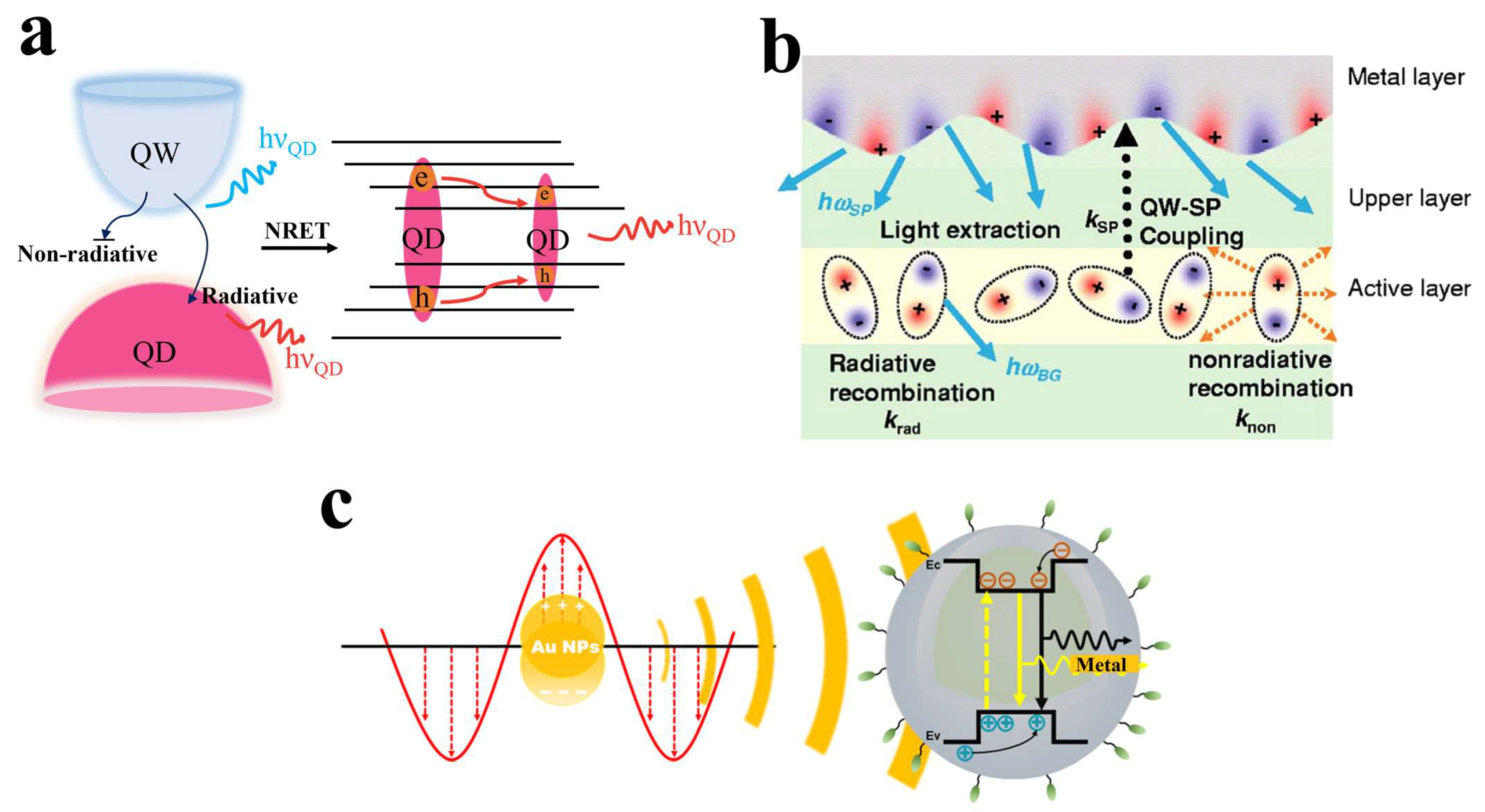
2.1. Non-Radiative Energy Transfer (NRET)

In the traditional process of QD excitation in quantum well (QW) luminescence, light is emitted from the QW, irradiating the QDs. The QDs absorb the photon energy for radiative transitions and emit low-frequency photons. This energy transfer process through light excitation is termed radiative energy transfer. Due to total internal reflection and dispersion of photons during the escape process, the number of photons emitted to the external world is very small, and QDs cannot absorb all the incident photons when absorbing light. Hence, this process results in some waste, leading to a small effective utilization of photons during absorption conversion and, ultimately, low CCE. Therefore, the NRET mechanism is introduced into QD-LEDs to increase CCE [46,47,48,49,50].
Figure 2a illustrates the basic process of NRET between QWs and QDs. The NRET process does not involve the absorption and emission of photons; instead, QDs directly absorb and relax the carrier energy from the QW within the band [51,52]. Thus, NRET reduces the absorption and re-emission of photons, significantly reducing the energy loss caused by these processes, thereby enhancing the color conversion efficiency and the quantum yield (QY) of QDs. However, NRET highly depends on the distance between QDs and the excitation light source, and the efficiency of energy transfer can be determined by the following equation [53,54,55]:
E N R E T = 1 / [ 1 + ( r / r 0 ) 4 ]
Here, ‘r’ represents the distance between the donor and acceptor, while ‘r0’ denotes the distance between the donor and acceptor when the energy transfer efficiency is 50%. For a specific system, the value of r0 remains constant. Therefore, shortening the distance between the QWs and QDs is crucial for enhancing the energy transfer rate and fully exploiting NRET.

2.2. Localized Surface Plasmon Resonance (LSPR)

When the size of metallic materials is much smaller than the wavelength of incident light, the electron cloud on the surface of the particles undergoes displacement relative to the atomic nucleus under the influence of the electric field of the light wave, forming localized plasmon resonances [56,57,58,59]. These resonances, matching the frequency of the incident light, result in a significant enhancement of the electromagnetic field on and near the metal surface. When the emitting materials (quantum wells and quantum dots) are close to metal NPs, their luminescence intensity and efficiency can be enhanced through LSPR, as illustrated in Figure 2b [44,57]. The electric field generated by localized surface plasmons (LSPs) is a transient field, decaying exponentially with increasing distance of field propagation [59,60]. In other words, the closer the material is to the light source, the stronger the coupling. Therefore, in μLEDs, shortening the distance between the QW and the metallic material is crucial for enhancing the efficiency of LSPR coupling.

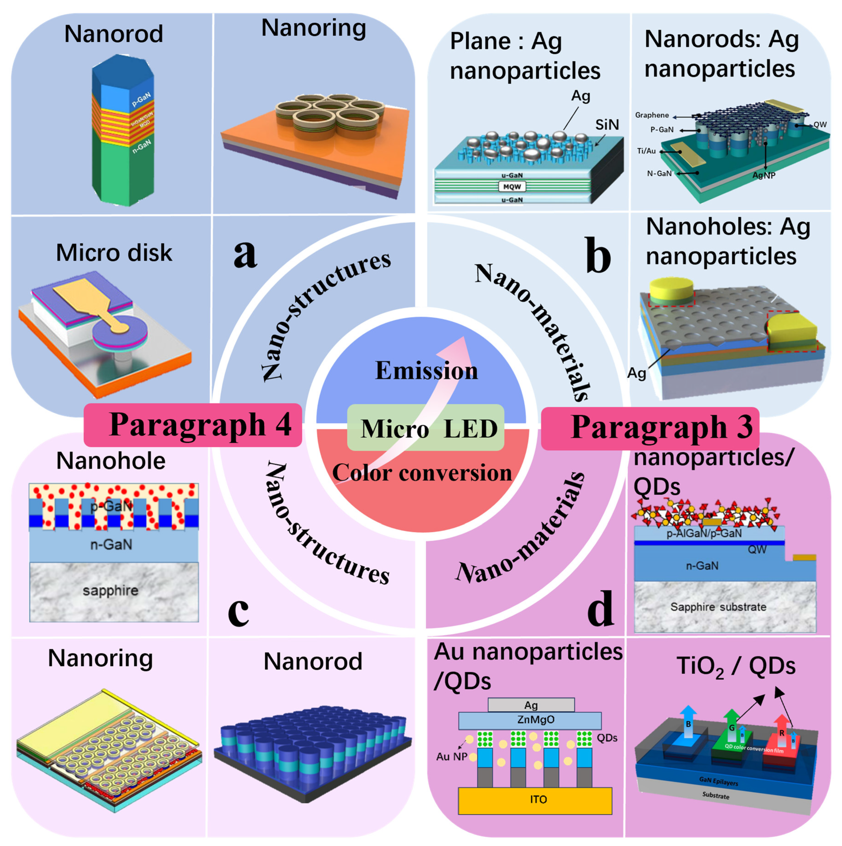
3. Using Nanomaterials to Enhance μLED Luminous Efficiency and Color Conversion Efficiency

Introducing specific nanomaterials into LEDs can increase light scattering and enhance the light extraction efficiency of LEDs. Many researchers have placed materials such as metal NPs [61,62] or polystyrene [63,64] on the surface of LEDs to act as LSPs or scattering agents to improve the light-emitting performance of LEDs. QDs are also nanomaterials that can absorb high-frequency photons and emit low-frequency photons, playing an important role in the full colorization of μLEDs. In this section, we will mainly introduce the recent applications of some nanomaterials in LEDs, such as metal NPs, colloidal QDs, and TiO2 NPs.

3.1. Metal Nanoparticles (NPs)

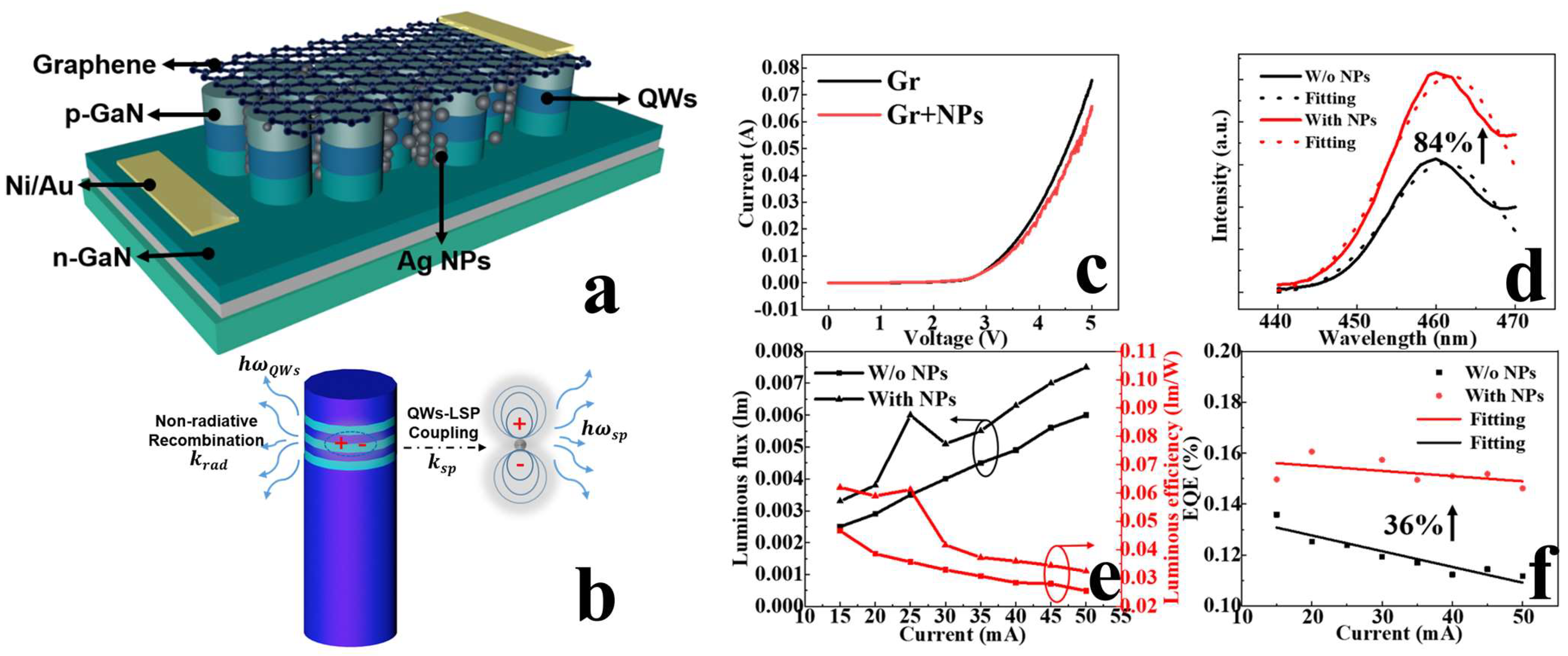
3.1.1. Using Ag NPs to Enhance Luminous Efficiency

Applying spin-coated Ag NPs on the surface and sidewalls of LEDs, matching the absorption resonance peak with the LED emission wavelength, and utilizing LSP resonance to enhance μLED luminous efficiency is a relatively simple method of using nanomaterials to improve device performance. In 2024, Sun et al. designed μLEDs of different sizes and spin coated Ag NPs on the top and sidewalls of these μLEDs [65]. Experimental results showed that for larger-sized devices, the electroluminescence (EL) intensity decreased after the addition of Ag NPs. This decrease was attributed to the fact that the Ag NPs on the surface of the μLED were too far away from the QW, exceeding 150 nm. This distance greatly exceeded the decay field range of LSPs; so, these Ag NPs only obstructed light emission and could not effectively couple with the emitting centers.
Meanwhile, in larger-sized devices, the proportion of sidewall area is relatively small, and the enhancement of luminous efficiency brought by LSP coupling at the sidewalls is not enough to compensate for the loss of light extraction caused by surface coverage. Therefore, there is a noticeable decrease in EL intensity. As the size of the μLED continues to shrink, the proportion of sidewall emission gradually increases, and the emitting area on the top surface gradually decreases. The benefits of suppressing non-radiative recombination through localized surface plasmon coupling slowly outweigh the reduction in light extraction caused by surface coverage. This is manifested in the increase in electroluminescence intensity. As shown in Figure 3d,e, as the mesa size decreases, the enhancement effect of LSPs on device emission intensity and EQE becomes more pronounced. In μLEDs with a mesa size of 20 × 20 μm2, compared to μLED samples without LSP coupling, EQE increased by approximately 8% under a high current density of 20,000 A/cm2. This study provides a valuable reference for the application of LSPs in enhancing the luminous performance of μLEDs.

3.1.2. Using Ag NPs to Enhance Color Conversion Efficiency

Enhancing the absorption efficiency of QDs for the excitation light source is a key aspect of applying QDs in full-color displays using μLEDs. Mixing metal NPs with QDs can enhance the energy conversion efficiency of QDs. In 2019, the Yang group coated different types and sizes of metal NPs mixed with QDs on the LED surface [43]; the absorption spectra of different types of metal NPs are shown in Figure 4b. The research results showed that Ag NPs, whose absorption resonance peak matches the QW emission wavelength, can enhance the emission intensity of QWs through QW-LSP coupling, thereby enhancing the emission intensity of QDs, as shown in Figure 4c.
The time-resolved photoluminescence (TRPL) of different devices is shown in Table 1, indicating that Ag NPs with absorption resonance peaks matching the QW emission wavelength can simultaneously increase the carrier decay rates of both QWs and QDs, leading to an overall improvement in energy conversion efficiency. This study fully demonstrates the positive role of LSP resonance in the emission of QDs. However, this experiment requires a sufficiently thin P-GaN layer to meet the requirements of LSP resonance for distance, which may have a significant impact on the performance of the LED [66].

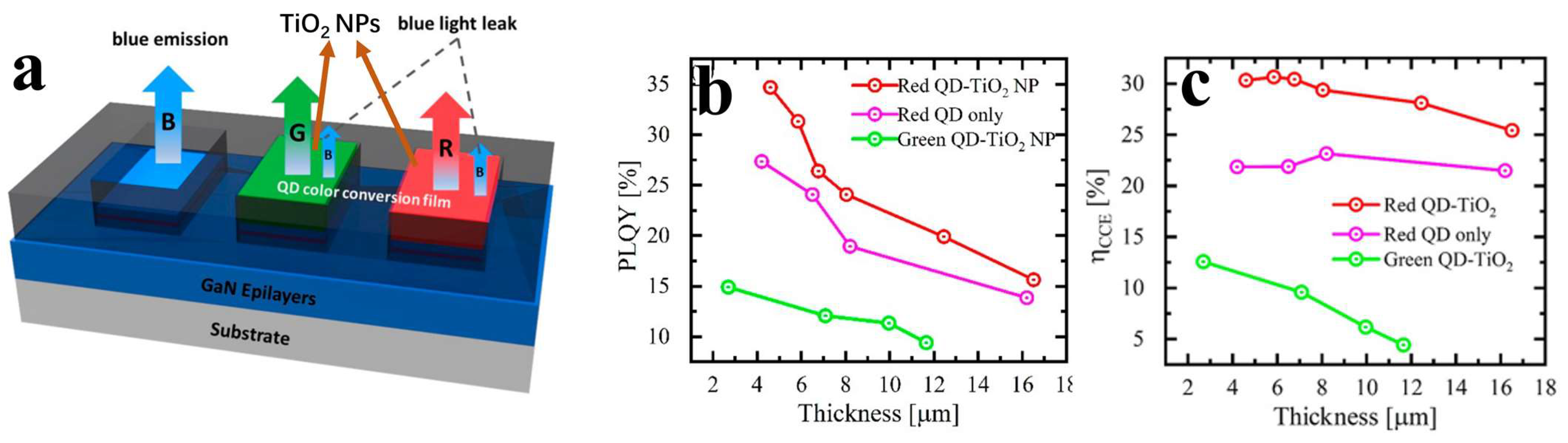
3.2. TiO2 Nanoparticles

In 2021, Kuo’s group added TiO2 NPs to red and green QDs [45], as shown in Figure 5a. Unlike LSPR, TiO2 enhances the scattering effect [67]; so, there is no need to deliberately thin the P-GaN layer. The experimental results showed that the scattering effect of TiO2 NPs enhanced the luminous intensity by more than 10%. Figure 5b shows the QY of two types of QDs, indicating a significant improvement in the QY of QDs after adding TiO2. The same change is also reflected in Figure 5c. This study suggests that the combination of QDs with other nanomaterials may enhance their QY and achieve better color conversion effects.
Numerous research results indicate that nanomaterials such as Ag NPs, polystyrene, metal oxide NPs, and others have a positive impact on enhancing the light-emitting performance of LEDs [68,69,70,71]. However, constrained by the LED’s own structure, these nanomaterials may not fully exert their maximum potential. Therefore, combining nanostructures with nanomaterials will provide greater assistance in improving the luminous efficiency and CCE of LEDs.

4. Using Nanostructures to Enhance μLED Luminous Efficiency and Color Conversion Efficiency

The nanostructures discussed in this review include nanorods, nanoholes, and nanorings. Nanorod structures can be formed by self-assembling nanospheres as etching hard masks or by molecular beam epitaxy (MBE). Nanohole structures are formed by a combination of nanoimprinting and inductively coupled plasma reactive ion etching (ICP-RIE). Nanoring structures can be prepared by using self-assembled nanospheres as etching hard masks or by a combination of electron beam lithography and ICP-RIE. Detailed fabrication processes are described in the following sections.

4.1. Nanoring Structures

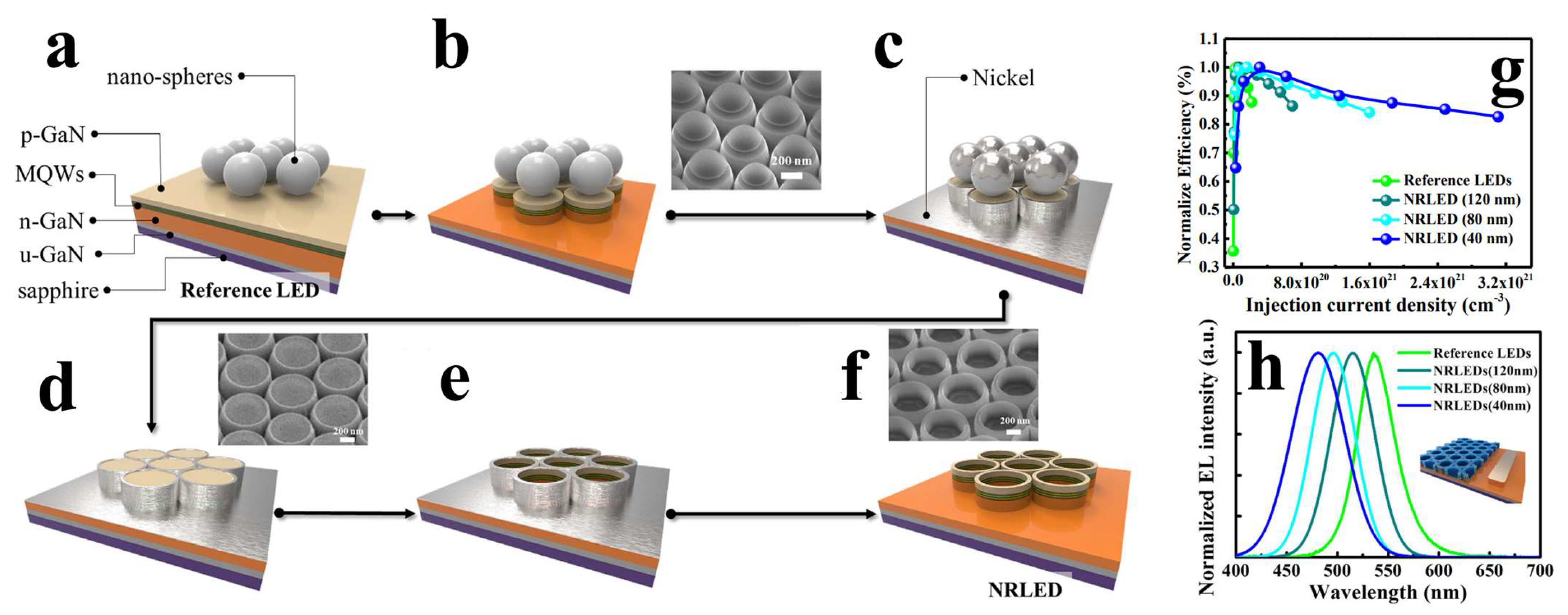
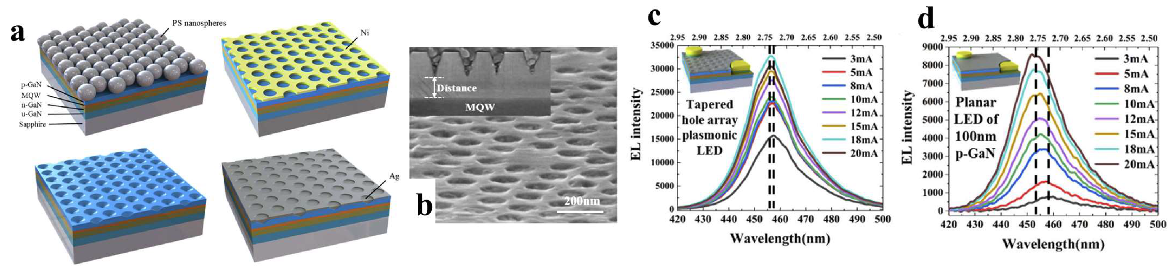
4.1.1. Using Nanorings to Enhance Luminous Efficiency

Introducing nanostructures into InGaN/GaN multiple quantum wells (MQWs) can significantly reduce the material’s strain relaxation, thereby improving QCSEs. Applying this concept to μLEDs can enhance the device’s luminous efficiency. Additionally, due to changes in the internal polarization field of the QWs, the emission wavelength of the QWs can be blueshifted. Precise control of the nanostructure size allows for accurate modulation of the emission wavelength range [29,72,73,74,75,76,77,78]. Based on this concept, in 2017, the Kuo research group fabricated nanoring arrays on LED epitaxial wafers by depositing nickel on the surface and etching out nanorings with an outer diameter of 800 nm and an inner diameter of approximately 700 nm [35], the fabrication process is illustrated in Figure 6a–f. The nanoring structure improved the strain inside the material, resulting in nanoring LEDs with higher internal quantum efficiency (IQE) than traditional LEDs. More importantly, by adjusting the width of the nanorings, they precisely modulated the emission wavelength of the nanoring LEDs and achieved emission in four different colors on the same epitaxial wafer. This successful practice not only addresses the decrease in IQE caused by improving the LED epitaxial internal polarization field but also provides new insights for achieving full-color μLEDs.

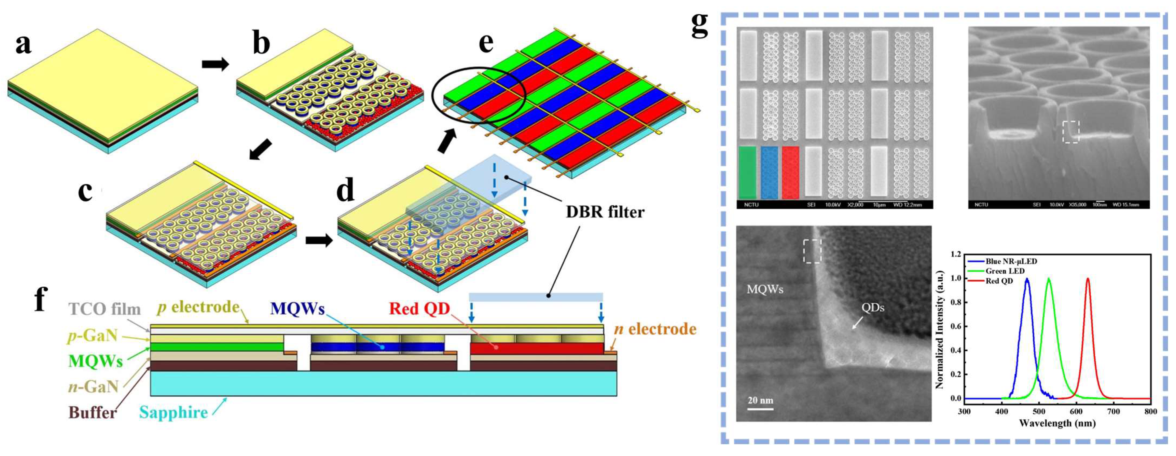
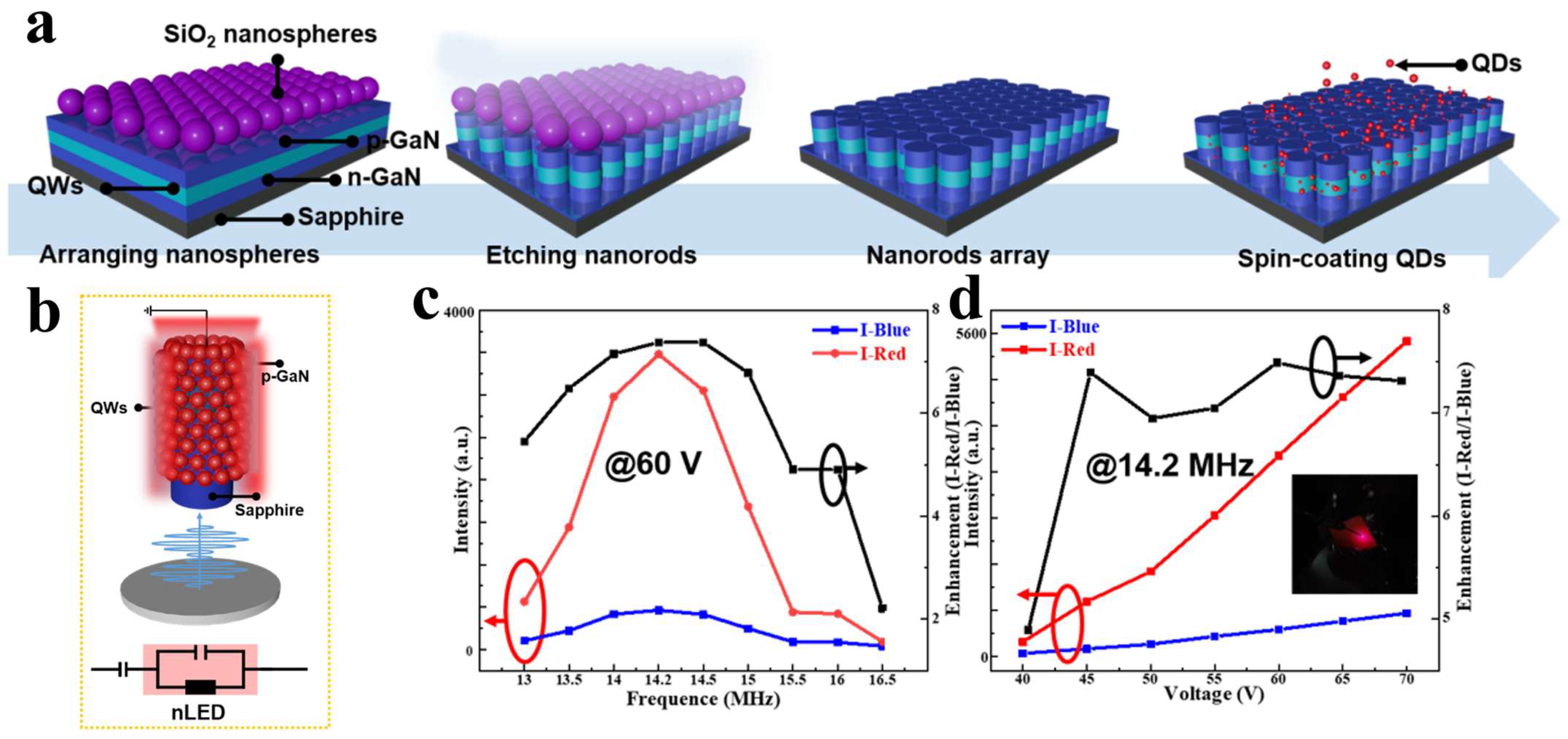
4.1.2. Using Nanorings to Enhance Color Conversion Efficiency

Based on the nanoring structure, LED emission wavelength can be precisely controlled, and the nanoring structure has significant advantages in shortening the distance between QDs and QWs. In 2019, Kuo’s research group etched nanoring arrays on GaN-based green LED epitaxial wafers and achieved single-chip integration of RGB μLEDs by adding red QDs to blue nanoring LEDs [41]. Figure 7a–f illustrates the process of achieving RGB using nanoring LEDs and QDs. In the experiment, the distance between the nanorings and QDs was small enough (as shown in Figure 7g), allowing full utilization of the advantages of NRET. This approach not only achieved full colorization but also enhanced the CCE, as demonstrated by the EL spectra of RGB sub-pixels shown in Figure 7g. It can be seen that combining nanoring structures with QDs effectively enables single-chip RGB emission on a homogeneous substrate.
Although nanoring structures can effectively alleviate internal strain and suppress QCSEs, their combination with QDs enables RGB emission in μLEDs. However, nanoring structures sacrifice a considerable amount of active area, resulting in low light intensity, and their fabrication process is relatively complex, making them difficult to apply to large-area full-color displays. These are the main factors constraining their further development [9].

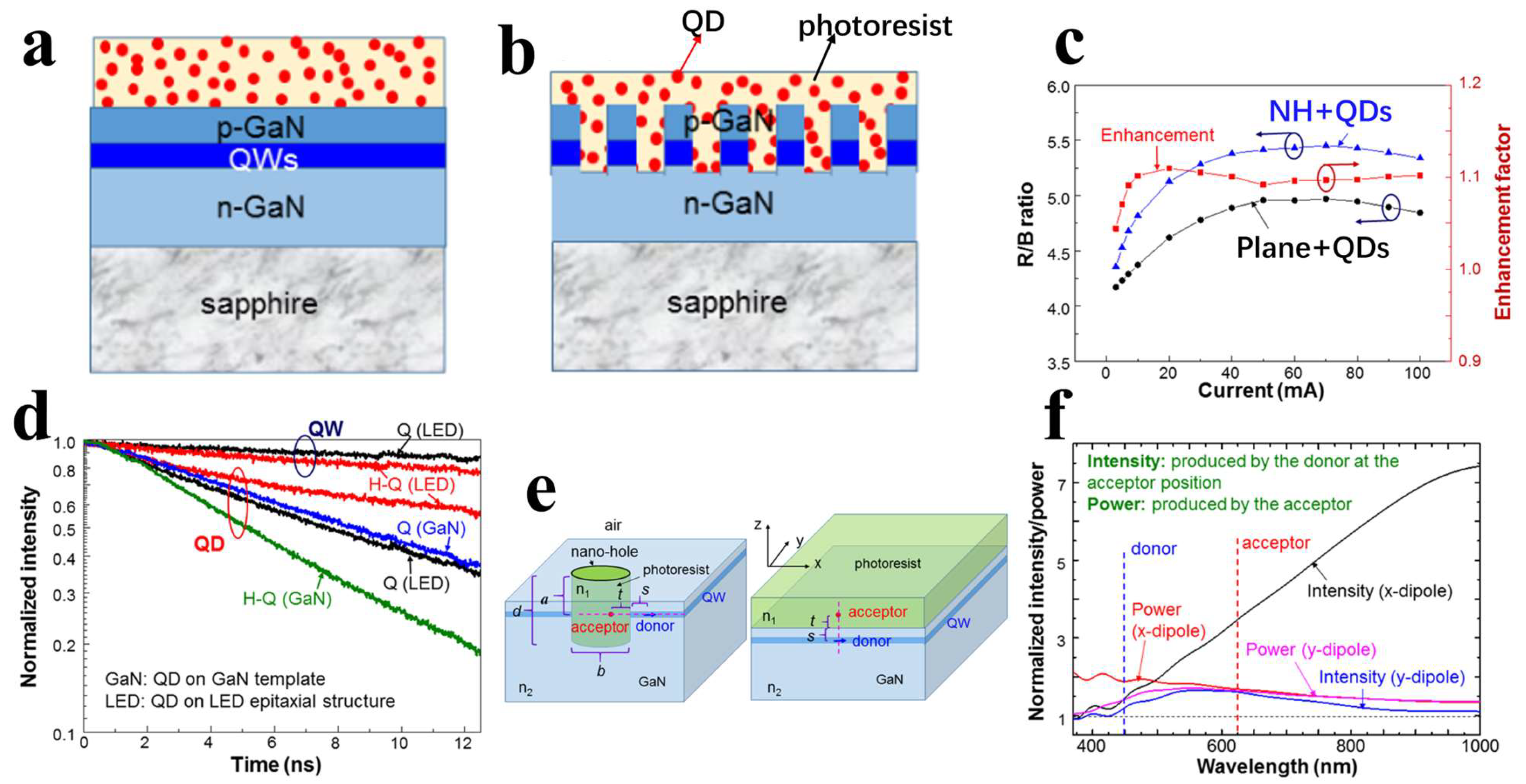
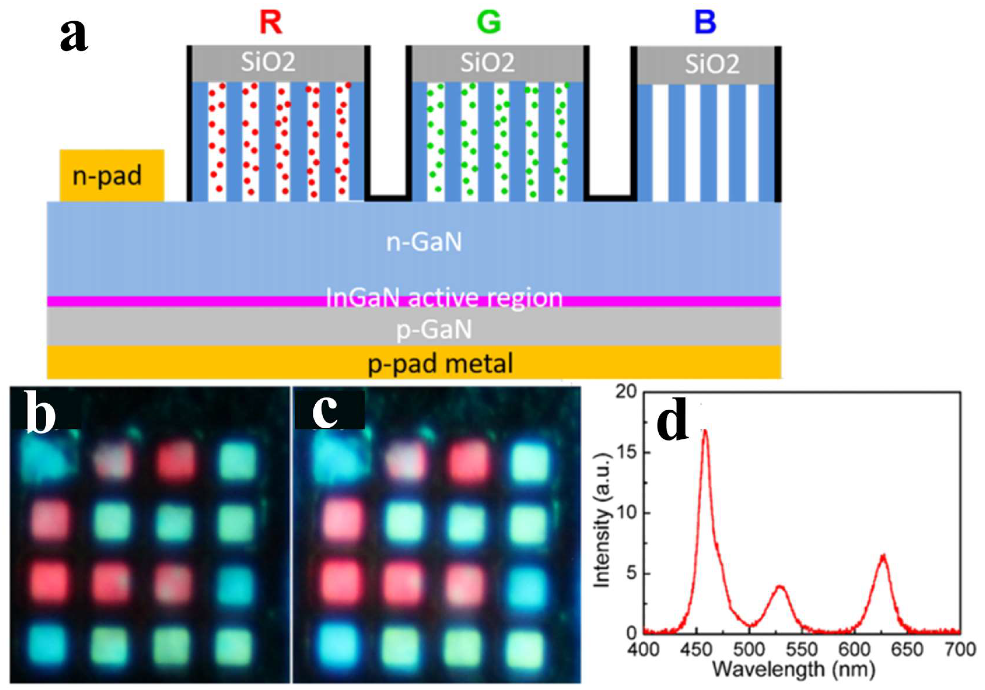
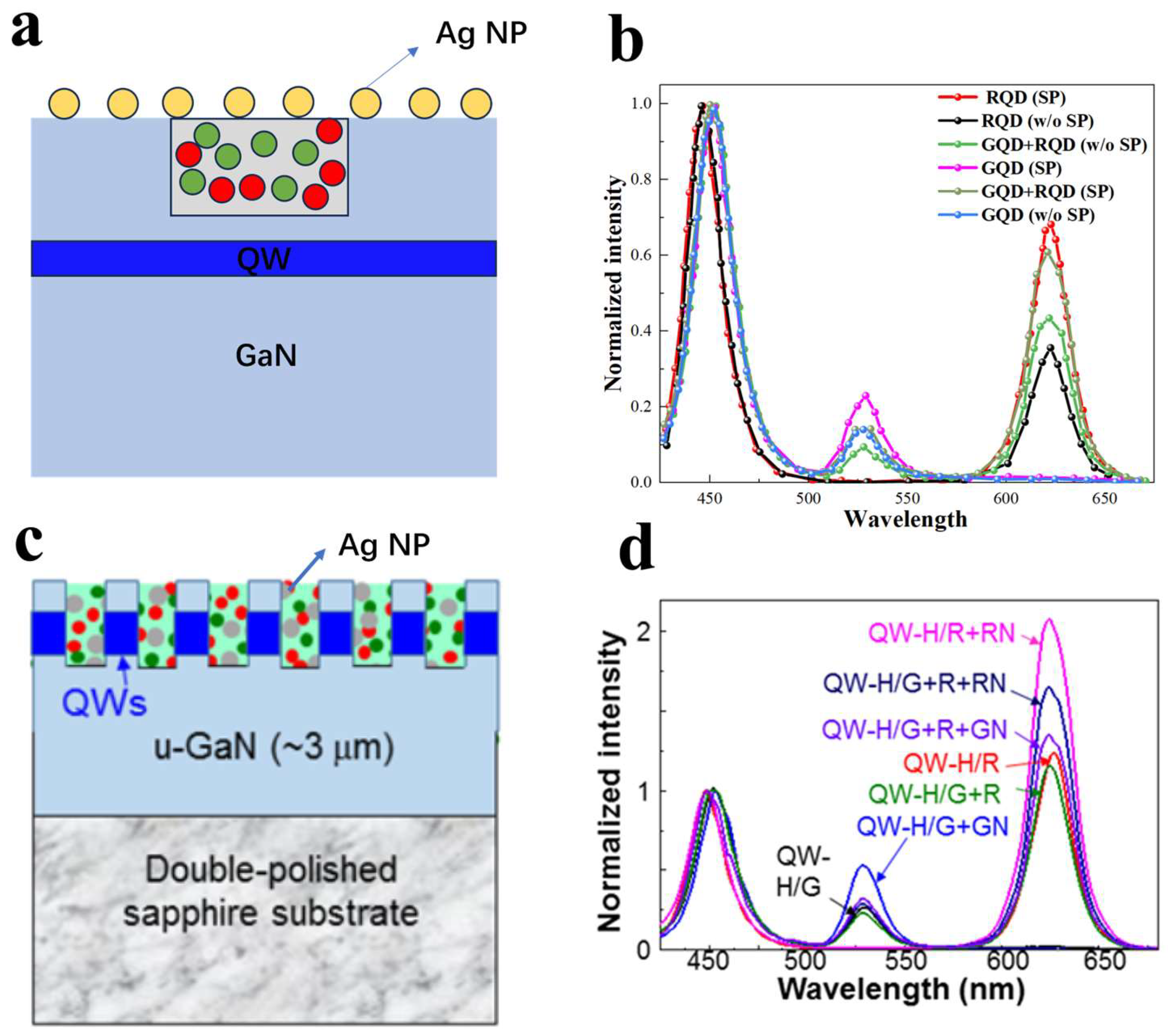
4.2. Nanohole Structure

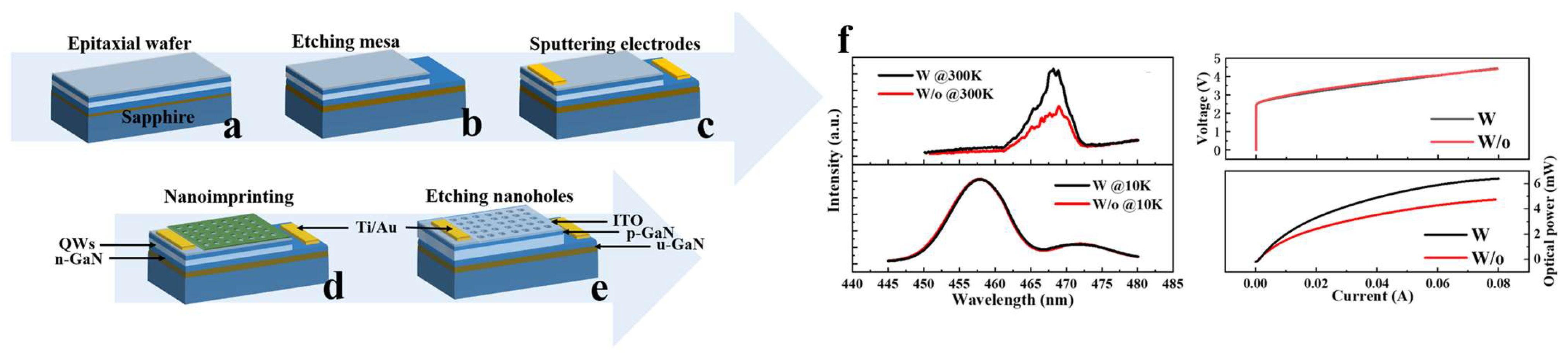
4.2.1. Using Nanoholes to Enhance Luminous Efficiency

Shortening the distance between QDs or metal NPs and MQWs is a primary approach for the application of NRET and LSPR in LEDs. Etching nanohole arrays on the LED surface to the active region allows for effective contact between QDs or metal NPs and MQWs, and the introduction of nanoholes enhances emission through the cavity effect [49,79,80,81]. Moreover, these nanohole arrays do not affect the conductivity of the P-GaN surface and can be used to prepare metal electrodes using traditional methods. In this section, we will mainly discuss the combination of nanohole arrays and nanomaterials to enhance the light emission efficiency and CCE of μLEDs.
In 2020, Yun et al. fabricated plasmon-enhanced LEDs with conical nanohole structures [39], as illustrated in Figure 8a. Figure 8b shows the surface and cross-sectional SEM images of the device, indicating that the conical nanohole structure shortened the distance between Ag and the MQW, significantly improving the plasmon coupling efficiency. Figure 8c,d displays the EL spectra of planar LEDs and conical-nanohole LSP-enhanced LEDs. Compared to traditional planar LEDs, the EL intensity increased by 16 times. The enhancement in long-range coupling efficiency stems from the accumulation of LSP energy at the apex of the metal cone and momentum loss provided by the ripple surface. Therefore, even with a thick p-GaN layer, LSP-enhanced LEDs with conical Ag structures can maintain high light emission efficiency. Additionally, due to the compensation of the polarization-induced electric field in the MQW by QW-LSP coupling, the efficiency of carrier recombination in the MQW is enhanced [82,83], and the reduction in QCSEs resulting from the decrease in internal stress in the LED material [84,85] significantly reduces the blue shift of the EL emission peak in LSP-enhanced LEDs. Consequently, with increasing current, LSP-enhanced LEDs with conical Ag structures can maintain higher light emission efficiency and a more stable operating state.
In 2022, the Guo and Sun research groups achieved surface plasmon-enhanced nanohole μLEDs (NH-μLED) using nanoimprint lithography [86]. The fabrication process is illustrated in Figure 9a–e. In contrast to the conical nanohole structures mentioned above, they etched nanoholes into the N-GaN layer. This deep nanohole structure allows direct contact between Ag and the MQW, thereby achieving more effective LSP–QWs coupling. The optical and electrical properties of the device are shown in Figure 9f. The IQE of NH-μLEDs filled with silver NPs increased by 12%, resulting in an overall enhancement in light output power.

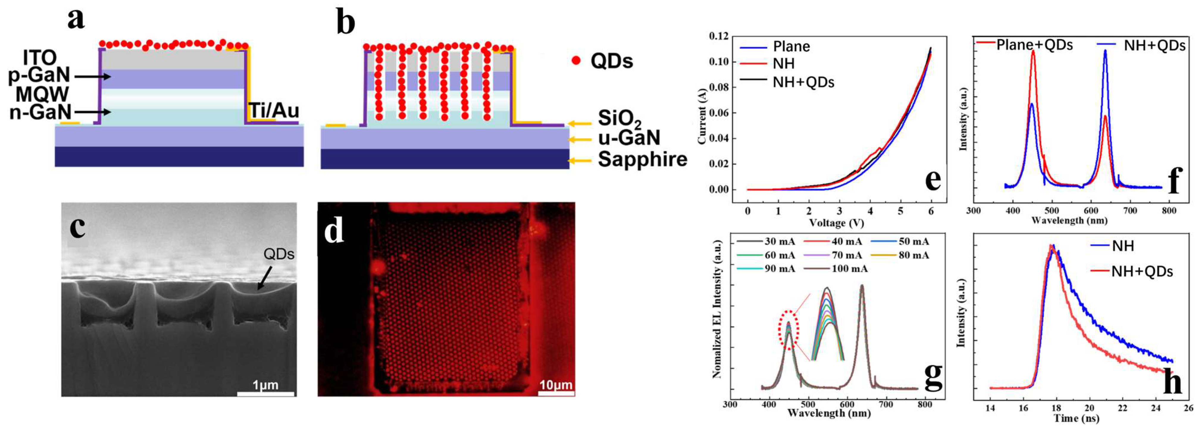
4.2.2. Using Nanoholes to Enhance Color Conversion Efficiency

Considering that NRET also heavily depends on the distance between QDs and QWs, the research group combined the nanohole structure with QDs to fabricate NH-QD-μLEDs [87]. Compared to conventional planar QD-μLEDs where QDs are spin coated on the surface (Figure 10a), the NH-QD-μLEDs (Figure 10b) exhibit similar electrical properties but demonstrate superior color conversion characteristics, with a CCE improvement of 118%. Additionally, as shown by the TRPL data in Figure 10g, the introduction of QDs into the nanoholes leads to a significant decrease in the carrier lifetime of the QWs. However, the deposition of QDs does not alter the intrinsic carrier dynamics of the QWs, indicating that the NH + QD structure provides an additional relaxation pathway for carriers in the QW, namely NRET.
In 2022, Yang’s research group utilized photolithography to encapsulate QDs within nanoholes, enabling the use of lithography techniques to design spatial QD distribution patterns on LED samples [40]; the planar structure and nanohole structure are shown in Figure 11a and Figure 11b, respectively. In addition to enhancing the efficiency of NRET between QWs and QDs, the nanohole structure introduced a nanoscale cavity effect representing a near-field Purcell effect. Through TRPL studies on QDs inserted into nanoholes within undoped GaN template structures, it was found that the emission efficiency of the inserted QDs significantly increased due to the nanoscale cavity effect. Figure 11e,f depicts the simulation results of the nanohole cavity effect, indicating a significant enhancement in the emission intensity of the emitting source with the nanohole structure, and this effect could also enhance NRET efficiency, especially for radiative dipoles in QWs perpendicular to the nanohole sidewalls. This research suggests that introducing nanostructures in LEDs not only enhances NRET efficiency but also modifies the radiative behavior of QDs through the Purcell effect [79], making their far-field emission stronger.
Incorporating nanohole structures into full-color displays can also demonstrate excellent performance. In 2021, Song et al. embedded multi-color QDs in nanoholes to achieve different emission colors and manufactured RGB μLED arrays with pixel sizes of approximately 35 × 35 μm2 [88]; the structure is shown in Figure 12a. Although the nanoholes were not etched into the active region, thus not inducing NRET between QWs and QDs, the nanoholes could induce strong light scattering effects, significantly increasing the optical transmission path for blue light [89,90]. This enhanced absorption and re-emission within the nanoholes, resulting in CCEs of 98% and 63% for the embedded red and green QDs, respectively.
If both LSPR and NRET can be utilized simultaneously, it would provide greater assistance in enhancing the performance of LEDs [91]. Yang’s research group designed two structures and characterized them using PL. The first structure, as shown in Figure 13a, involves nanoholes etched to a depth not exceeding the thickness of the P-GaN layer, filled with red and green QDs and covered with a layer of Ag serving as LSP [92]. PL testing (shown in Figure 13b) indicates that both red and green PL intensities are enhanced by the SP coupling, clearly demonstrating the enhanced color conversion from QWs to QDs. Furthermore, the research group etched nanoholes into the N-GaN layer and filled them with QDs and Ag (shown in Figure 13c) [93], allowing for closer contact and coupling between QWs, QDs, and LSPs. The PL spectra of different samples, as shown in Figure 13d, indicate that when only one type of QD is present, the LSP matching the emission wavelength of the current QD significantly enhances its emission intensity. When both red and green QDs are present, the LSP matching the emission wavelength of the red QD contributes more prominently to the overall CCE.

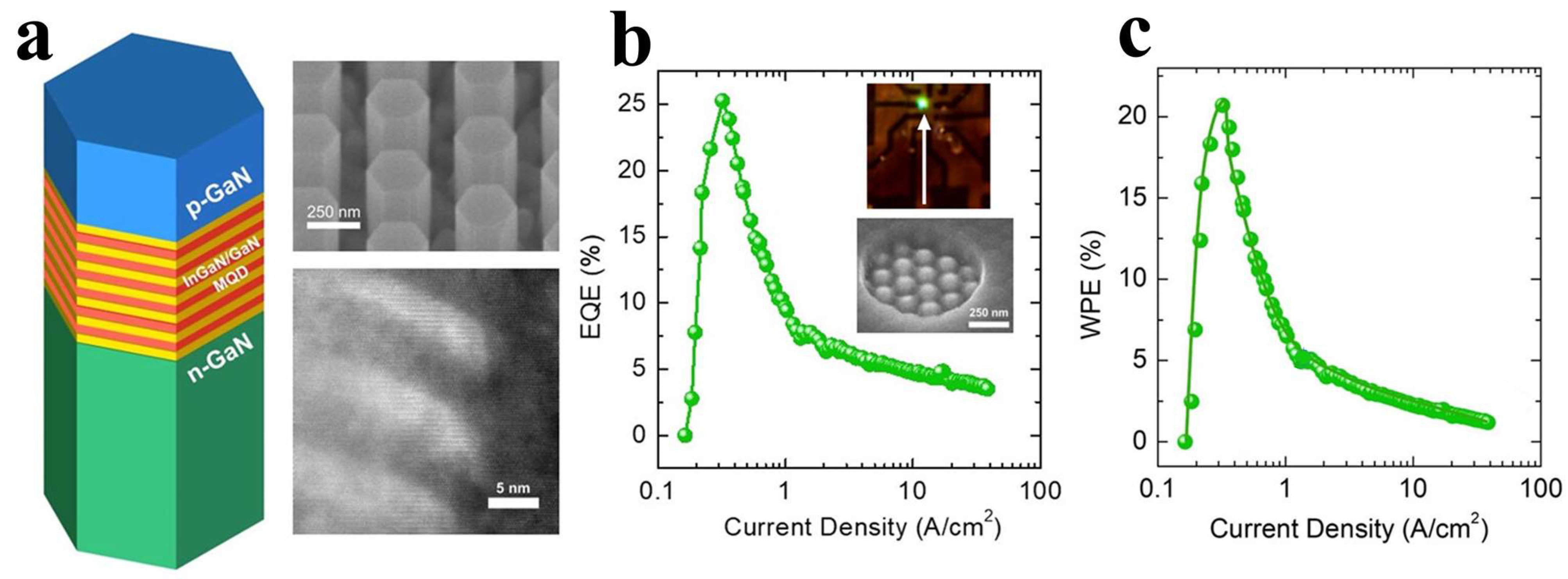
4.3. Nanorod Structure

4.3.1. Using Nanorods to Enhance Luminous Efficiency

The nanorod structure can also play a similar role as nanoholes and nanorings. Moreover, compared to other nanostructures, nanorod structures can save more active area. Additionally, nanorods provide more escape paths for photons, similar to the effect of photonic crystals, thereby the enhancing light extraction efficiency of LEDs [94,95,96,97]. In recent years, many researchers have combined nanomaterials with nanorod structures to enhance the performance of μLEDs.
In 2023, the Mi research group demonstrated a submicron-sized green LED, and based on this, fabricated a μLED based on a nanorod array [34]. The individual nanorod structure and nanorod array are shown in Figure 14a, Figure 14b and Figure 14c demonstrate their EQE and wall-plug efficiency (WPE), which are 25.2% and 20.7%, respectively. The enhanced performance of the LED in this study is attributed to the nanorod structure achieving strain relaxation, utilizing semi-polar planes to minimize polarization effects and forming nanoscale quantum confinement to enhance electron–hole wavefunction overlap.
The combination of nanorod structures with nanomaterials can significantly enhance the light emission efficiency of μLEDs. Guo and Sun’s research groups achieved improvements in both the light emission efficiency and CCE of μLEDs by integrating nanorod structures with Ag NPs [38] and QDs [42], respectively.
The research groups filled the gaps between nanorods with Ag NPs, ensuring full contact between Ag NPs and the sidewalls of nanorods. They then transferred a layer of graphene as a transparent conductive layer to connect independent nanorods, thereby utilizing the coupling between LSPs and QWs and the high conductivity and high transmittance of graphene to prepare an LSP-enhanced μLED [38]. Figure 15a illustrates the device structure, while Figure 15b depicts the schematic of the coupling between nanorods and LSPR. At room temperature, the PL intensity of the nanorod-µLED structure assisted by LSPs (before graphene transfer) increased by approximately 84%, and the EQE of the nanorod-μLED after graphene transfer remained 36% higher. This study applied LSPs and graphene to nanorod LEDs, enhancing the light emission efficiency of μLEDs and addressing the issue of non-contiguous nanorods, thereby opening up prospects for the application of LSPs in nanorod LEDs.

4.3.2. Using Nanorods to Enhance Color Conversion Efficiency

The combination of nanostructures and nanomaterials not only enhances the luminous efficiency of μLEDs, but also enables efficient color conversion when combined with QDs [98]. Figure 16a illustrates the fabrication process of the device. In this study, silica nanospheres were utilized as self-assembled masks for etching, resulting in the formation of uniformly distributed nanorods. Subsequently, QDs were filled into the nanorods, achieving ultra-high color conversion efficiency through NRET [42]. The schematic diagram of the driving circuit for QD-NR structure is shown in Figure 16b, unlike traditional direct current driving methods, a single-side contact alternating current driving method was adopted, eliminating electrode growth and simplifying the fabrication process. Test results demonstrated that maximum electroluminescent intensity and CCE were achieved when applying an alternating current with a frequency of 14.2 MHz, as shown in Figure 16c and Figure 16d. Under the conditions of 60 V and 14.2 MHz, the color conversion efficiency of the QD-based nanorod LED (nLED) used in this work was approximately 86.67%. This research confirms that the nanorod structure exposes more QWs for contact with QDs, thereby enabling the NRET mechanism between QDs and QWs to play a significant role in color conversion for μLEDs. Furthermore, the single-side contact alternating current driving method adopted in this experiment simplifies the fabrication process of μLEDs. Through the principle of special carrier injection, it can improve the crosstalk between μLED pixels and enhance the luminous efficiency of μLEDs [99,100,101,102].
Although nanorod arrays can release stress to the maximum extent and increase LEE by sacrificing fewer active regions and combining them with certain nanomaterials can enhance LED performance, the discontinuity between nanorod arrays presents challenges for current spreading and electrode fabrication. Single-side contact alternating current driving is not practical for actual production. Currently, there are two main methods for growing nanorod electrodes. One method involves spin coating glass or filling nanorod gaps with silica for planarization before electrode growth [29,72,75,103], while the other method involves directly transferring graphene as a transparent conductive layer, followed by metal electrode sputtering [28,38,74,104]. Regardless of the method used, it undoubtedly increases production costs, which is a major reason why nanorod structures are difficult to apply in actual production.

5. Challenges and Prospects

μLED undoubtedly represents a new display technology for the future; yet, true commercialization remains unrealized due to issues such as luminous brightness, full colorization, and mass transfer. The application of nanomaterials and nanostructures in LEDs presents a pathway to addressing these challenges. Based on the aforementioned studies, nanomaterials such as metal NPs, TiO2 NPs, and QDs can assist μLEDs in achieving high-brightness emission and provide new avenues for full colorization. By designing and introducing nanostructures, the optical, electrical, and thermal properties of LED devices can be altered, thereby improving their luminous efficiency, color conversion efficiency, and stability.
For instance, the utilization of nanostructures such as nanorods, nanoholes, and nanorings can enhance LEE, reduce internal reflection and refraction losses, release epitaxial stress, suppress QCSEs, and enhance luminous efficiency. Additionally, nanostructures can reduce the distance between nanomaterials and MQWs, introducing LSP coupling and NRET mechanisms, thereby reducing energy loss and maximizing the enhancement effects of nanomaterials on LED performance.
Although the application of nanomaterials and nanostructures in LEDs can enhance luminous efficiency and CCE, there are also several drawbacks. Metal NPs are prone to oxidation, and if they aggregate in large quantities, they can cause charge energy transfer, leading to overall fluorescence quenching [57]. QDs, as color conversion materials, have poor thermal stability and reliability. Prolonged use in full-color arrays can result in a decrease in CCE [105,106,107].
Similarly, the aforementioned nanostructures also have their own limitations. Nanoring and nanohole structures sacrifice a significant active area, which may lead to a decrease in overall luminous efficiency. Moreover, nanorings and nanorods are discontinuous, posing challenges for the fabrication of metal electrodes. These factors constrain the industrial application of these structures.
As μLED display technology continues to evolve, there are still many core technologies for achieving full-color displays, such as mass transfer [108] and three-color stacking [109,110]. Arrays produced using these methods are more reliable and suitable for large-scale production. The future development of μLED display technology will likely revolve around these two techniques.
Beyond display applications, μLEDs hold enormous potential in the visible light domain due to their ultra-fast light pulses and extremely high modulation bandwidth [111,112,113]. In particular, with the continuous development of 5G and 6G networks in recent years, μLED visible light communication (VLS) is poised to have a significant application market. The nanomaterials and nanostructures discussed in this review can also be applied in μLED VLS to further increase its modulation bandwidth and transmission rate or to realize optical communication at different wavelengths.

Author Contributions

Conceptualization, A.F. and W.G.; validation, J.S., W.G. and A.F.; formal analysis, A.F.; investigation, A.F. and J.L.; resources, J.S.; data curation, Z.D.; writing—original draft preparation, A.F.; writing—review and editing, A.F.; visualization, H.X.; supervision, P.T.; project administration, W.G.; funding acquisition, J.S. All authors have read and agreed to the published version of the manuscript.

Funding

This research was funded by National Key Research and Development Program of China (Nos. 2023YFB3608703 and 2023YFB3608700), Fujian Science & Technology Innovation Laboratory for Optoelectronic Information of China (Nos. 2021ZZ122 and 2020ZZ110), and Fujian provincial projects (Nos. 2021HZ0114 and 2021J01583).

Data Availability Statement

Not applicable.

Conflicts of Interest

The authors declare no conflicts of interest.

References

  1. Lee, T.-Y.; Chen, L.-Y.; Lo, Y.-Y.; Swayamprabha, S.S.; Kumar, A.; Huang, Y.-M.; Chen, S.-C.; Zan, H.-W.; Chen, F.-C.; Horng, R.-H.; et al. Technology and Applications of Micro-LEDs: Their Characteristics, Fabrication, Advancement, and Challenges. ACS Photonics 2022, 9, 3017–3026. [Google Scholar] [CrossRef]
  2. Ding, K.; Avrutin, V.; Izyumskaya, N.; Özgür, Ü.; Morkoç, H. Micro-LEDs, a Manufacturability Perspective. Appl. Sci. 2019, 9, 1206. [Google Scholar] [CrossRef]
  3. Parbrook, P.J.; Corbett, B.; Han, J.; Seong, T.-Y.; Amano, H. Micro-Light Emitting Diode: From Chips to Applications. Laser Photonics Rev. 2021, 15, 2000133. [Google Scholar] [CrossRef]
  4. Chiou, E. TrendForce 2023 Micro LED Market Trend and Technology Cost Analysis; TrendForce: Taipei City, China, 2023; Available online: https://www.trendforce.com/research/download/RP231130BR (accessed on 30 November 2023).
  5. Zhou, X.; Tian, P.; Sher, C.-W.; Wu, J.; Liu, H.; Liu, R.; Kuo, H.-C. Growth, transfer printing and colour conversion techniques towards full-colour micro-LED display. Prog. Quantum Electron. 2020, 71, 100263. [Google Scholar] [CrossRef]
  6. Park, S.-C.; Fang, J.; Biswas, S.; Mozafari, M.; Stauden, T.; Jacobs, H.O. A First Implementation of an Automated Reel-to-Reel Fluidic Self-Assembly Machine. Adv. Mater. 2014, 26, 5942–5949. [Google Scholar] [CrossRef]
  7. Yoon, J.; Lee, S.-M.; Kang, D.; Meitl, M.A.; Bower, C.A.; Rogers, J.A. Heterogeneously Integrated Optoelectronic Devices Enabled by Micro-Transfer Printing. Adv. Opt. Mater. 2015, 3, 1313–1335. [Google Scholar] [CrossRef]
  8. Gandrothula, S.; Kamikawa, T.; Shapturenka, P.; Anderson, R.; Wong, M.; Zhang, H.; Speck, J.S.; Nakamura, S.; Denbaars, S.P. Optical and electrical characterizations of micro-LEDs grown on lower defect density epitaxial layers. Appl. Phys. Lett. 2021, 119, 142103. [Google Scholar] [CrossRef]
  9. Olivier, F.; Tirano, S.; Dupré, L.; Aventurier, B.; Largeron, C.; Templier, F. Influence of size-reduction on the performances of GaN-based micro-LEDs for display application. J. Lumin. 2017, 191, 112–116. [Google Scholar] [CrossRef]
  10. Liou, J.C.; Yang, C.F. Design and fabrication of micro-LED array with application-specific integrated circuits (ASICs) light emitting display. Microsyst. Technol. 2018, 24, 4089–4099. [Google Scholar] [CrossRef]
  11. Horng, R.-H.; Chen, Y.-F.; Wang, C.-H.; Chen, H.-Y. Development of Metal Bonding for Passive Matrix Micro-LED Display Applications. IEEE Electron Device Lett. 2021, 42, 1017–1020. [Google Scholar] [CrossRef]
  12. Li, P.; Zhang, X.; Qi, L.; Lau, K.M. Full-color micro-display by heterogeneous integration of InGaN blue/green dual-wavelength and AlGaInP red LEDs. Opt. Express 2022, 30, 23499–23510. [Google Scholar] [CrossRef] [PubMed]
  13. Ahmed, K. Micro LED Display: Technology and Manufacturing Challenges. SPIE Proc. 2021, 11610, 1161003. [Google Scholar] [CrossRef]
  14. Hang, S.; Chuang, C.-M.; Zhang, Y.; Chu, C.; Tian, K.; Zheng, Q.; Wu, T.; Liu, Z.; Zhang, Z.-H.; Li, Q.; et al. A review on the low external quantum efficiency and the remedies for GaN-based micro-LEDs. J. Phys. D Appl. Phys. 2021, 54, 153002. [Google Scholar] [CrossRef]
  15. Xu, F.; Tao, T.; Zhang, D.; Zhang, Y.; Sang, Y.; Yu, J.; Zhi, T.; Zhuang, Z.; Xie, Z.; Zhang, R.; et al. Wafer-Scale Monolithic Integration of Blue Micro-Light-Emitting Diodes and Green/Red Quantum Dots for Full-Color Displays. IEEE Electron Device Lett. 2023, 44, 1320–1323. [Google Scholar] [CrossRef]
  16. Han, L.; Ogier, S.; Li, J.; Sharkey, D.; Yin, X.; Baker, A.; Carreras, A.; Chang, F.; Cheng, K.; Guo, X. Wafer-scale organic-on-III-V monolithic heterogeneous integration for active-matrix micro-LED displays. Nat. Commun. 2023, 14, 6985. [Google Scholar] [CrossRef] [PubMed]
  17. Qi, L.; Li, P.; Zhang, X.; Wong, K.M.; Lau, K.M. Monolithic full-color active-matrix micro-LED micro-display using InGaN/AlGaInP heterogeneous integration. Light. Sci. Appl. 2023, 12, 258. [Google Scholar] [CrossRef] [PubMed]
  18. Han, H.-V.; Lin, H.-Y.; Lin, C.-C.; Chong, W.-C.; Li, J.-R.; Chen, K.-J.; Yu, P.; Chen, T.-M.; Chen, H.-M.; Lau, K.-M.; et al. Resonant-enhanced full-color emission of quantum-dot-based μLED display technology. Opt. Express 2015, 23, 32504–32515. [Google Scholar] [CrossRef]
  19. Kou, J.; Shen, C.C.; Shao, H.; Che, J.; Hou, X.; Chu, C.; Tian, K.; Zhang, Y.; Zhang, Z.H.; Kuo, H.C. Impact of the surface recombination on InGaN/GaN-based blue micro-light emitting diodes. Opt. Express 2019, 27, A643–A653. [Google Scholar] [CrossRef] [PubMed]
  20. Horng, R.-H.; Ye, C.-X.; Chen, P.-W.; Iida, D.; Ohkawa, K.; Wu, Y.-R.; Wuu, D.-S. Study on the effect of size on InGaN red micro-LEDs. Sci. Rep. 2022, 12, 1324. [Google Scholar] [CrossRef]
  21. Wang, X.; Zhao, X.; Takahashi, T.; Ohori, D.; Samukawa, S. 3.5 × 3.5 μm2 GaN blue micro-light-emitting diodes with negligible sidewall surface nonradiative recombination. Nat. Commun. 2023, 14, 7569. [Google Scholar] [CrossRef]
  22. Bulashevich, K.A.; Kulik, A.V.; Karpov, S.Y. Optimal ways of colour mixing for high-quality white-light LED sources. Phys. Status Solidi A 2015, 212, 914–919. [Google Scholar] [CrossRef]
  23. Hwang, D.; Mughal, A.; Pynn, C.D.; Nakamura, S.; DenBaars, S.P. Sustained high external quantum efficiency in ultrasmall blue III–nitride micro-LEDs. Appl. Phys. Express 2017, 10, 032101. [Google Scholar] [CrossRef]
  24. Hou, M.; Wang, H.; Miao, Y.; Xu, H.; Guo, Z.; Chen, Z.; Liao, X.; Li, L.; Li, J.; Guo, K. Highly Efficient Deep-Blue Electroluminescence from a A−π–D−π–A Structure Based Fluoresence Material with Exciton Utilizing Efficiency above 25%. ACS Appl. Energy Mater. 2018, 1, 3243–3254. [Google Scholar] [CrossRef]
  25. Huang, Y.; Hsiang, E.-L.; Deng, M.-Y.; Wu, S.-T. Mini-LED, Micro-LED and OLED displays: Present status and future perspectives. Light. Sci. Appl. 2020, 9, 105. [Google Scholar] [CrossRef]
  26. Ponce, F.; Bour, D. Nitride-based semiconductors for blue and green light-emitting devices. Nature 1997, 386, 351–359. [Google Scholar] [CrossRef]
  27. Fujii, T.; Gao, Y.; Sharma, R.; Hu, E.L.; DenBaars, S.P.; Nakamura, S. Increase in the extraction efficiency of GaN-based light-emitting diodes via surface roughening. Appl. Phys. Lett. 2004, 84, 855–857. [Google Scholar] [CrossRef]
  28. Xu, K.; Xu, C.; Xie, Y.; Deng, J.; Zhu, Y.; Guo, W.; Mao, M.; Xun, M.; Chen, M.; Zheng, L.; et al. GaN nanorod light emitting diodes with suspended graphene transparent electrodes grown by rapid chemical vapor deposition. Appl. Phys. Lett. 2013, 103, 222105. [Google Scholar] [CrossRef]
  29. Ke, M.-Y.; Wang, C.-Y.; Chen, L.-Y.; Chen, H.-H.; Chiang, H.-L.; Cheng, Y.-W.; Hsieh, M.-Y.; Chen, C.-P.; Huang, J.-J. Application of Nanosphere Lithography to LED Surface Texturing and to the Fabrication of Nanorod LED Arrays. IEEE J. Sel. Top. Quantum Electron. 2009, 15, 1242–1249. [Google Scholar] [CrossRef]
  30. Tsai, S.-C.; Lu, C.-H.; Liu, C.-P. Piezoelectric effect on compensation of the quantum-confined Stark effect in InGaN/GaN multiple quantum wells based green light-emitting diodes. Nano Energy 2016, 28, 373–379. [Google Scholar] [CrossRef]
  31. Chan, C.C.S.; Reid, B.P.L.; Taylor, R.A.; Zhuang, Y.; Shields, P.A.; Allsopp, D.W.E.; Jia, W. Optical studies of the surface effects from the luminescence of single GaN/InGaN nanorod light emitting diodes fabricated on a wafer scale. Appl. Phys. Lett. 2013, 102, 129–2214. [Google Scholar] [CrossRef]
  32. Zhang, S.; Zhang, J.; Gao, J.; Wang, X.; Zheng, C.; Zhang, M.; Wu, X.; Xu, L.; Ding, J.; Quan, Z.; et al. Efficient emission of InGaN-based light-emitting diodes: Toward orange and red. Photon. Res. 2020, 8, 1671–1675. [Google Scholar] [CrossRef]
  33. Fan, K.; Tao, J.; Zhao, Y.; Li, P.; Sun, W.; Zhu, L.; Lv, J.; Qin, Y.; Wang, Q.; Liang, J.; et al. Size effects of AlGaInP red vertical micro-LEDs on silicon substrate. Results Phys. 2022, 36, 105449. [Google Scholar] [CrossRef]
  34. Pandey, A.; Min, J.; Reddeppa, M.; Malhotra, Y.; Xiao, Y.; Wu, Y.; Sun, K.; Mi, Z. An Ultrahigh Efficiency Excitonic Micro-LED. Nano Lett. 2023, 23, 1680–1687. [Google Scholar] [CrossRef] [PubMed]
  35. Wang, S.W.; Hong, K.B.; Tsai, Y.L.; Teng, C.H.; Tzou, A.J.; Chu, Y.C.; Lee, P.T.; Ku, P.C.; Lin, C.C.; Kuo, H.C. Wavelength tunable InGaN/GaN nano-ring LEDs via nano-sphere lithography. Sci. Rep. 2017, 7, 42962. [Google Scholar] [CrossRef] [PubMed]
  36. Mei, Y.; Xie, M.; Yang, T.; Hou, X.; Ou, W.; Long, H.; Ying, L.; Liu, Y.; Weng, G.; Chen, S.; et al. Improvement of the Emission Intensity of GaN-Based Micro-Light Emitting Diodes by a Suspended Structure. ACS Photonics 2022, 9, 3967–3973. [Google Scholar] [CrossRef]
  37. Fadila, A.; Ou, Y.; Iida, D.; Kamiyama, S.; Petersen, P.M.; Ou, H. Combining surface plasmonic and light extraction enhancement on InGaN quantum-well light-emitters. Nanoscale 2016, 8, 16340. [Google Scholar] [CrossRef] [PubMed]
  38. Du, Z.; Feng, H.; Liu, Y.; Tang, P.; Qian, F.; Sun, J.; Guo, W.; Song, J.; Chen, E.; Guo, T.; et al. Localized surface plasmon coupling nanorods with graphene as a transparent conductive electrode for micro light-emitting diodes. IEEE Electron Device Lett. 2022, 43, 2133–2136. [Google Scholar] [CrossRef]
  39. Wang, X.; Tian, Z.; Zhang, M.; Li, Q.; Su, X.; Zhang, Y.; Hu, P.; Li, Y.; Yun, F. Enhanced coupling efficiency and electrical property in surface plasmon-enhanced light-emitting diodes with the tapered Ag structure. Opt. Express 2020, 28, 35708–35715. [Google Scholar] [CrossRef]
  40. Huang, Y.-Y.; Li, Z.-H.; Lai, Y.-C.; Chen, J.-C.; Wu, S.-H.; Yang, S.; Kuo, Y.; Yang, C.-C.; Hsu, T.-C.; Lee, C.-L. Nanoscale-cavity enhancement of color conversion with colloidal quantum dots embedded in the surface nano-holes of a blue-emitting light-emitting diode. Opt. Express 2022, 30, 31322–31335. [Google Scholar] [CrossRef]
  41. Chen, H.; Shen, C.; Wu, T.; Liao, Z.; Chen, L.; Zhou, J.; Lee, C.; Lin, C.; Lin, C.; Sher, C.; et al. Full-color monolithic hybrid quantum dot nanoring micro light-emitting diodes with improved efficiency using atomic layer deposition and nonradiative resonant energy transfer. Photonics Res. 2019, 7, 416–422. [Google Scholar] [CrossRef]
  42. Du, Z.; Wang, K.; Sun, J.; Guo, W.; Wu, C.; Lin, C.; Yan, Q. Ultrahigh color conversion efficiency nano-light-emitting diode with single electrical contact. IEEE Trans. Electron Devices 2023, 70, 1156–1161. [Google Scholar] [CrossRef]
  43. Wang, Y.-T.; Liu, C.-W.; Chen, P.-Y.; Wu, R.-N.; Ni, C.-C.; Cai, C.-J.; Kiang, Y.-W.; Yang, C.C. Color conversion efficiency enhancement of colloidal quantum dot through its linkage with synthesized metal nanoparticle on a blue light-emitting diode. Opt. Lett. 2019, 44, 5691–5694. [Google Scholar] [CrossRef]
  44. Zhang, X.; Hu, H.; Qie, Y.; Lin, L.; Guo, T.; Li, F. Boosting the Efficiency of High-Resolution Quantum Dot Light-Emitting Devices Based on Localized Surface Plasmon Resonance. ACS Appl. Mater. Interfaces 2024, 16, 13219–13224. [Google Scholar] [CrossRef] [PubMed]
  45. Hyun, B.-R.; Sher, C.-W.; Chang, Y.-W.; Lin, Y.; Liu, Z.; Kuo, H.-C. Dual Role of Quantum Dots as Color Conversion Layer and Suppression of Input Light for Full-Color Micro-LED Displays. J. Phys. Chem. Lett. 2021, 12, 6946–6954. [Google Scholar] [CrossRef] [PubMed]
  46. Achermann, M.; Petruska, M.; Kos, S.; Smith, D.L.; Koleske, D.D.; Klimov, V.I. Energy-transfer pumping of semiconductor nanocrystals using an epitaxial quantum well. Nature 2004, 429, 642–646. [Google Scholar] [CrossRef]
  47. Chanyawadee, S.; Lagoudakis, P.G.; Harley, R.T.; Charlton, M.D.B.; Talapin, D.V.; Huang, H.W.; Lin, C.-H. Increased Color-Conversion Efficiency in Hybrid Light-Emitting Diodes utilizing Non-Radiative Energy Transfer. Adv. Mater. 2010, 22, 602–606. [Google Scholar] [CrossRef] [PubMed]
  48. Achermann, M.; Petruska, M.A.; Koleske, D.D.; Crawford, M.H.; Klimov, V.I. Nanocrystal-Based Light-Emitting Diodes Utilizing High-Efficiency Nonradiative Energy Transfer for Color Conversion. Nano Lett. 2006, 6, 1396–1400. [Google Scholar] [CrossRef]
  49. Krishnan, C.; Brossard, M.; Lee, K.-Y.; Huang, J.-K.; Lin, C.-H.; Kuo, H.-C.; Charlton, M.D.B.; Lagoudakis, P.G. Hybrid photonic crystal light-emitting diode renders 123% color conversion effective quantum yield. Optica 2016, 3, 503–509. [Google Scholar] [CrossRef]
  50. Ghataora, S.; Smith, R.M.; Athanasiou, M.; Wang, T. Electrically Injected Hybrid Organic/Inorganic III-Nitride White Light-Emitting Diodes with Nonradiative Förster Resonance Energy Transfer. ACS Photonics 2018, 5, 642–647. [Google Scholar] [CrossRef]
  51. Zhang, F.; Liu, J.; You, G.; Zhang, C.; Mohney, S.E.; Park, M.J.; Kwak, J.S.; Wang, Y.; Koleske, D.D.; Xu, J. Nonradiative energy transfer between colloidal quantum dot-phosphors and nanopillar nitride LEDs. Opt. Express 2012, 20, A333–A339. [Google Scholar] [CrossRef]
  52. Zhuang, Z.; Guo, X.; Liu, B.; Hu, F.; Li, Y.; Tao, T.; Dai, J.; Zhi, T.; Xie, Z.; Chen, P.; et al. High Color Rendering Index Hybrid III-Nitride/Nanocrystals White Light-Emitting Diodes. Adv. Funct. Mater. 2016, 26, 36–43. [Google Scholar] [CrossRef]
  53. Pons, T.; Medintz, I.L.; Sapsford, K.E.; Higashiya, S.; Grimes, A.F.; English, D.S.; Mattoussi, H. On the Quenching of Semi-conductor Quantum Dot Photoluminescence by Proximal Gold Nanoparticles. Nano Lett. 2007, 7, 3157–3164. [Google Scholar] [CrossRef] [PubMed]
  54. Sahoo, H. Förster resonance energy transfer–A spectroscopic nanoruler: Principle and applications. J. Photochem. Photobiol. C Photochem. Rev. 2011, 12, 20–30. [Google Scholar] [CrossRef]
  55. Krishnan, C.; Mercier, T.; Rahman, T.; Piana, G.; Brossard, M.; Yagafarov, T.; To, A.; Pollard, M.E.; Shaw, P.; Bagnall, D.M. Efficient light harvesting in hybrid quantum dot–interdigitated back contact solar cells via resonant energy transfer and luminescent downshifting. Nanoscale 2019, 11, 18837–18844. [Google Scholar] [CrossRef] [PubMed]
  56. Okamoto, K.; Niki, I.; Scherer, A.; Narukawa, Y.; Mukai, T.; Kawakami, Y. Surface plasmon enhanced spontaneous emission rate of quantum wells probed by time-resolved photoluminescence spectroscopy. Appl. Phys. Lett. 2005, 87, 071102. [Google Scholar] [CrossRef]
  57. Gao, N.; Huang, K.; Li, J.; Li, S.; Yang, X.; Kang, J. Surface-plasmon-enhanced deep-UV light emitting diodes based on AlGaN multi-quantum wells. Sci. Rep. 2012, 2, 816. [Google Scholar] [CrossRef] [PubMed]
  58. Shi, Z.; Li, Y.; Li, S.; Li, X.; Wu, D.; Xu, T.; Tian, Y.; Chen, Y.; Zhang, Y.; Zhang, B.; et al. Localized Surface Plasmon Enhanced All-Inorganic Perovskite Quantum Dot Light-Emitting Diodes Based on Coaxial Core/Shell Heterojunction Architecture. Adv. Funct. Mater. 2018, 28, 1707031. [Google Scholar] [CrossRef]
  59. Sanz, J.M.; Ortiz, D.; Osa, R.A.; Saiz, J.M.; González, F.; Brown, A.S.; Losurdo, M.; Everitt, H.O.; Moreno, F. UV Plasmonic Behavior of Various Metal Nanoparticles in the Near- and Far-Field Regimes: Geometry and Substrate Effects. J. Phys. Chem. C 2013, 117, 19606–19615. [Google Scholar] [CrossRef]
  60. Barnes, W.L. Turning the Tables on Surface Plasmons. Nature 2004, 3, 588–589. [Google Scholar] [CrossRef]
  61. Zhang, S.; He, R.; Duo, Y.; Chen, R.; Wang, L.; Wang, J.; Wei, T. Plasmon-enhanced deep ultraviolet Micro-LED arrays for solar-blind communications. Opt. Lett. 2023, 48, 3841–3844. [Google Scholar] [CrossRef]
  62. Jiang, N.; Chen, Y.; Lv, B.; Jiang, K.; Zhang, S.; Lu, S.; Li, S.; Tao, T.; Sun, X.; Li, D. Plasmonic-enhanced efficiency of AlGaN-based deep ultraviolet LED by graphene/Al nanoparticles/graphene hybrid structure. Opt. Lett. 2023, 48, 3175–3178. [Google Scholar] [CrossRef] [PubMed]
  63. Cheng, W.C.; Huang, S.Y.; Chen, Y.J.; Wang, C.S.; Lin, H.Y.; Wu, T.M.; Horng, R.H. AlGaInP red LEDs with hollow hemi-spherical polystyrene arrays. Sci. Rep. 2018, 8, 911. [Google Scholar] [CrossRef] [PubMed]
  64. Zhan-Xu, C.; Wei, W.; Ying-Ji, H.; Geng-Yan, C.; Yong-Zhu, C. Light-extraction enhancement of GaN-based LEDs by closely-packed nanospheres monolayer. Acta Phys. Sin. 2015, 64, 148502. [Google Scholar] [CrossRef]
  65. Du, Z.; Sun, J.; Feng, H.; Tang, P.; Guo, W.; Han, K.; Chen, E.; Guo, T.; Song, J.; Yan, Q. Efficiency enhancement of micro-light-emitting diode with shrinking size by localized surface plasmons coupling. Appl. Phys. B 2024, 130, 36. [Google Scholar] [CrossRef]
  66. Chang, W.-M.; Huang, J.-J.; Yao, Y.-F.; Kiang, Y.-W.; Yang, C.-C. Emission Efficiency Dependence on the p-GaN Thickness in a High Indium InGaN/GaN Quantum-Well Light-Emitting Diode. IEEE Photon. Technol. Lett. 2011, 23, 1757–1759. [Google Scholar] [CrossRef]
  67. Cho, I.S.; Chen, Z.; Forman, A.J.; Kim, D.R.; Rao, P.M.; Jaramillo, T.F.; Zheng, X. Branched TiO2 Nanorods for Photoelectrochemical Hydrogen Production. Nano Lett. 2011, 11, 4978–4984. [Google Scholar] [CrossRef] [PubMed]
  68. Hossain, M.K.; Kitahama, Y.; Huang, G.G.; Han, X.; Ozaki, Y. Surface-enhanced Raman scattering: Realization of localized surface plasmon resonance using unique substrates and methods. Anal. Bioanal. Chem. 2009, 394, 1747–1760. [Google Scholar] [CrossRef] [PubMed]
  69. Kim, S.-K.; Lee, S.-H.; Yoon, S.-Y.; Jo, D.-Y.; Kim, H.-M.; Kim, Y.; Park, S.M.; Yang, H. Localized surface plasmon-enhanced blue electroluminescent device based on ZnSeTe quantum dots and AuAg nanoparticles. Inorg. Chem. Front. 2022, 9, 3138–3147. [Google Scholar] [CrossRef]
  70. Wang, B.Z.; Chua, S.J. Enhanced light output from light emitting diodes with two-dimensional cone-shape nanostructured surface. J. Vac. Sci. Technol. B 2013, 31, 032205. [Google Scholar] [CrossRef]
  71. Yang, Y.; Zheng, Y.; Cao, W.; Titov, A.; Hyvonen, J.; Manders, J.R.; Xue, J.; Holloway, P.H.; Qian, L. High-efficiency light-emitting devices based on quantum dots with tailored nanostructures. Nat. Photon. 2015, 9, 259–266. [Google Scholar] [CrossRef]
  72. Kim, H.-M.; Cho, Y.-H.; Lee, H.; Kim, S.I.; Ryu, S.R.; Kim, D.Y.; Kang, T.W.; Chung, K.S. High-Brightness Light Emitting Diodes Using Dislocation-Free Indium Gallium Nitride/Gallium Nitride Multiquantum-Well Nanorod Arrays. Nano Lett. 2004, 4, 1059–1062. [Google Scholar] [CrossRef]
  73. Chen, H.-S.; Yeh, D.-M.; Lu, Y.-C.; Chen, C.-Y.; Huang, C.-F.; Tang, T.-Y.; Yang, C.C.; Wu, C.-S.; Chen, C.-D. Strain relaxation and quantum confinement in InGaN/GaN nanoposts. Nanotechnology 2006, 17, 1454–1458. [Google Scholar] [CrossRef]
  74. Li, Z.; Kang, J.; Zhang, Y.; Liu, Z.; Wang, L.; Lee, X.; Li, X.; Yi, X.; Zhu, H.; Wang, G. The fabrication of GaN-based nanorod light-emitting diodes with multilayer graphene transparent electrodes. J. Appl. Phys. 2013, 113, 234302. [Google Scholar] [CrossRef]
  75. Chen, L.-Y.; Huang, Y.-Y.; Chang, C.-H.; Sun, Y.-H.; Cheng, Y.-W.; Ke, M.-Y.; Chen, C.-P.; Huang, J. High performance InGaN/GaN nanorod light emitting diode arrays fabricated by nanosphere lithography and chemical mechanical polishing processes. Opt. Express 2010, 18, 7664–7669. [Google Scholar] [CrossRef] [PubMed]
  76. Li, Q.; Westlake, K.R.; Crawford, M.H.; Lee, S.R.; Koleske, D.D.; Figiel, J.J.; Cross, K.C.; Fathololoumi, S.; Mi, Z.; Wang, G.T. Optical performance of top-down fabricated InGaN/GaN nanorod light emitting diode arrays. Opt. Express 2011, 19, 25528–25534. [Google Scholar] [CrossRef] [PubMed]
  77. Bae, S.-Y.; Kong, D.-J.; Lee, J.-Y.; Seo, D.-J.; Lee, D.-S. Size-controlled InGaN/GaN nanorod array fabrication and optical characterization. Opt. Express 2013, 21, 16854–16862. [Google Scholar] [CrossRef] [PubMed]
  78. Nakashima, S.; Sugioka, K.; Ito, T.; Takai, H.; Midorikawa, K. Fabrication of periodic nano-hole array on GaN surface by fs laser for improvement of extraction efficiency in blue LED. Phys. Procedia 2010, 5A, 203–211. [Google Scholar] [CrossRef]
  79. Kuo, Y.; Yang, C.C. Theoretical/Numerical Studies of the Nanoscale-Cavity Effects on Dipole Emission, Förster Resonance Energy Transfer, and Surface Plasmon Coupling. Plasmonics 2024, 19, 273–285. [Google Scholar] [CrossRef]
  80. Poirier-Richard, H.-P.; Couture, M.; Brule, T.; Masson, J.-F. Metal-enhanced fluorescence and FRET on nanohole arrays excited at angled incidence. Analyst 2015, 140, 4792–4798. [Google Scholar] [CrossRef]
  81. Purcell, E.M. Spontaneous Emission Probabilities at Radio Frequencies. In Confined Electrons and Photons; Burstein, E., Weisbuch, C., Eds.; NATO ASI Series; Springer: Boston, MA, USA, 1995; Volume 340, Chapter 40. [Google Scholar] [CrossRef]
  82. Qi, Y.D.; Liang, H.; Wang, D.; Lu, Z.D.; Tang, W.; Lau, K.M. Comparison of blue and green InGaN/GaN multiple-quantum-well light-emitting diodes grown by metalorganic vapor phase epitaxy. Appl. Phys. Lett. 2005, 86, 101903. [Google Scholar] [CrossRef]
  83. Tateishi, K.; Wang, P.; Ryuzaki, S.; Funato, M.; Kawakami, Y.; Okamoto, K.; Tamada, K. Micro-photoluminescence mapping of surface plasmon enhanced light emissions from InGaN/GaN quantum wells. Appl. Phys. Lett. 2017, 111, 172105. [Google Scholar] [CrossRef]
  84. Sun, L.; Zhang, S.; Liu, F.; Han, M. Influence of localized surface plasmons on carrier dynamics in InGaN/GaN quantum wells covered with Ag nanoparticles for enhanced photoluminescence. Superlattices Microstruct. 2015, 86, 418–424. [Google Scholar] [CrossRef]
  85. Cho, C.-Y.; Park, S.-J. Enhanced optical output and reduction of the quantum-confined Stark effect in surface plasmon-enhanced green light-emitting diodes with gold nanoparticles. Opt. Express 2016, 24, 7488. [Google Scholar] [CrossRef] [PubMed]
  86. Du, Z.; Chen, E.; Feng, H.; Qian, F.; Xiong, F.; Tang, P.; Guo, W.; Song, J.; Yan, Q.; Guo, T.; et al. Efficiency improvement of GaN-based micro-light-emitting diodes embedded with Ag NPs into a periodic arrangement of nano-hole channel structure by ultra close range localized surface plasmon coupling. Nanotechnology 2022, 33, 495202. [Google Scholar] [CrossRef] [PubMed]
  87. Du, Z.; Li, D.; Guo, W.; Xiong, F.; Tang, P.; Zhou, X.; Zhang, Y.; Guo, T.; Yan, Q.; Sun, J. Quantum Dot Color Conversion Efficiency Enhancement in Micro-Light-Emitting Diodes by Non-Radiative Energy Transfer. IEEE Electron Device Lett. 2021, 42, 1184–1187. [Google Scholar] [CrossRef]
  88. Song, J.; Kang, J.-h.; Han, J. Monolithic RGB Micro-Light-Emitting Diodes Fabricated with Quantum Dots Embedded inside Nanoporous GaN. ACS Appl. Electron. Mater. 2021, 3, 4877–4881. [Google Scholar] [CrossRef]
  89. Muskens, O.L.; Rivas, J.G.; Algra, R.E.; Bakkers, E.P.A.M.; Lagendijk, A. Design of Light Scattering in Nanowire Materials for Photovoltaic Applications. Nano Lett. 2008, 8, 2638–2642. [Google Scholar] [CrossRef]
  90. Muskens, O.L.; Diedenhofen, S.L.; Kaas, B.C.; Algra, R.E.; Bakkers, E.P.A.M.; Gómez Rivas, J.; Lagendijk, A. Large Photonic Strength of Highly Tunable Resonant Nanowire Materials. Nano Lett. 2009, 9, 930–934. [Google Scholar] [CrossRef] [PubMed]
  91. Zhuang, Z.; Li, C.; Zhang, Y.; Liu, B.; Zhang, X.; Fan, A.; Chen, S.; Lu, L.; Cui, Y. Influence of plasmonic resonant wavelength on energy transfer from an InGaN quantum well to quantum dots. Appl. Phys. Lett. 2021, 118, 202103. [Google Scholar] [CrossRef]
  92. Yang, S.; Lai, Y.-C.; Feng, H.-Y.; Lee, Y.-C.; Li, Z.-H.; Wu, S.-H.; Lin, Y.-S.; Hsieh, H.-Y.; Chu, C.-J.; Chen, W.-C.; et al. Enhanced Color Conversion of Quantum Dots Located in the Hot Spot of Surface Plasmon Coupling. IEEE Photonics Technol. Lett. 2023, 35, 273–276. [Google Scholar] [CrossRef]
  93. Chen, C.-H.; Kuo, S.-Y.; Feng, H.-Y.; Li, Z.-H.; Yang, S.; Wu, S.-H.; Hsieh, H.-Y.; Lin, Y.-S.; Lee, Y.-C.; Chen, W.-C.; et al. Photon color conversion enhancement of colloidal quantum dots inserted into a subsurface laterally-extended GaN nano-porous structure in an InGaN/GaN quantum-well template. Opt. Express 2023, 31, 6327–6341. [Google Scholar] [CrossRef] [PubMed]
  94. Bavencove, A.-L.; Tourbot, G.; Garcia, J.; Désières, Y.; Gilet, P.; Levy, F.; André, B.; Gayral, B.; Daudin, B.; Dang, L.S. Submicrometre resolved optical characterization of green nanowire-based light emitting diodes. Nanotechnology 2011, 22, 345705. [Google Scholar] [CrossRef] [PubMed]
  95. Yu, Z.-G.; Zhao, L.-X.; Wei, X.-C.; Wang, J.-X.; Li, J.-M. Influence of SiO2 or SiNx passivation on the electrical properties of GaN-based nanorod LEDs. In Proceedings of the 2013 10th China International Forum on Solid State Lighting (ChinaSSL), Beijing, China, 10–12 November 2013; pp. 291–294. [Google Scholar] [CrossRef]
  96. Bavencove, A.-L.; Tourbot, G.; Pougeoise, E.; Garcia, J.; Gilet, P.; Levy, F.; André, B.; Feuillet, G.; Gayral, B.; Daudin, B.; et al. GaN-based nanowires: From nanometric-scale characterization to light emitting diodes. Phys. Stat. Sol. A 2010, 207, 1425–1427. [Google Scholar] [CrossRef]
  97. Kim, S.-U.; Um, D.-Y.; Oh, J.-K.; Chandran, B.; Lee, C.-R.; Ra, Y.-H. Structural Engineering in a Microscale Laser Diode with InGaN Tunnel-Junction Nanorods. ACS Photonics 2023, 10, 1053–1059. [Google Scholar] [CrossRef]
  98. Kotlyar, K.P.; Morozov, I.A.; Shubina, K.Y.; Berezovskaya, T.N.; Dragunova, A.S.; Kryzhanovskaya, N.V.; Kudryashov, D.A.; Lihachev, A.I.; Nashchekin, A.V.; Soshnikov, I.P.; et al. InGaN/GaN QDs nanorods for light emitters: Processing and properties. AIP Conf. Proc. 2019, 2064, 030006. [Google Scholar] [CrossRef]
  99. Wang, K.; Liu, Y.; Chen, R.; Wu, C.; Zhou, X.; Zhang, Y.; Liu, Z.; Guo, T. Light-Pulse Splitting from Nano-Light-Emitting Diodes Operating in Noncarrier Injection Mode. IEEE Electron Device Lett. 2021, 42, 1033–1036. [Google Scholar] [CrossRef]
  100. Wang, K.; Chen, P.; Chen, J.; Liu, Y.; Wu, C.; Sun, J.; Zhou, X.; Zhang, Y.; Guo, T. Alternating current electroluminescence from GaN-based nanorod light-emitting diodes. Opt. Laser Technol. 2021, 140, 107044. [Google Scholar] [CrossRef]
  101. Zhang, D.; Xu, F.; Sang, Y.; Yu, J.; Tao, T.; Zhuang, Z.; Zhi, T.; Yan, Y.; Liu, B.; Zhang, R.; et al. Dominant Mechanism of GaN-Based Single Contact Micro-LED Driven by AC Power. IEEE Electron Device Lett. 2023, 44, 468–471. [Google Scholar] [CrossRef]
  102. Wang, K.; Li, W.; Chen, R.; Zhang, Y.; Zhou, X.; Ye, Y.; Guo, T.; Wu, C. High-Density LED Array Based on Epitaxial Slice Damage-Free Process and Its Single-Contact Operation Mode with Low Crosstalk. IEEE Electron Device Lett. 2023, 44, 1865–1868. [Google Scholar] [CrossRef]
  103. Koester, R.; Sager, D.; Quitsch, W.-A.; Pfingsten, O.; Poloczek, A.; Blumenthal, S.; Keller, G.; Prost, W.; Bacher, G.; Tegude, F.-J. High-Speed GaN/GaInN Nanowire Array Light-Emitting Diode on Silicon(111). Nano Lett. 2015, 15, 2318–2323. [Google Scholar] [CrossRef]
  104. Jeon, D.; Choi, W.M.; Shin, H.; Yoon, S.; Choi, J.; Jang, L.; Lee, I. Nanopillar InGaN/GaN light emitting diodes integrated with homogeneous multilayer graphene electrodes. J. Mater. Chem. 2011, 21, 17688. [Google Scholar] [CrossRef]
  105. Li, Z.-T.; Song, C.-J.; Du, X.-W.; Xuan, J.; Li, J.-S.; Tang, Y. Study on the Photoluminescence Intensity, Thermal Performance, and Color Purity of Quantum Dot Light-Emitting Diodes Using a Pumping-Light Absorber. IEEE Trans. Electron. Devices 2020, 67, 2418–2424. [Google Scholar] [CrossRef]
  106. Elahi, A.M.N.; Pei, Z.; Yu, P.; Xu, J. Thermal and Photochemical Stability Studies of Color-Converted MicroLED Microdisplay Panels. IEEE Photonics J. 2023, 15, 1–6. [Google Scholar] [CrossRef]
  107. Huang, Y.-M.; Singh, K.J.; Liu, A.-C.; Lin, C.-C.; Chen, Z.; Wang, K.; Lin, Y.; Liu, Z.; Wu, T.; Kuo, H.-C. Advances in Quantum-Dot-Based Displays. Nanomaterials 2020, 10, 1327. [Google Scholar] [CrossRef]
  108. Anwar, A.R.; Sajjad, M.T.; Johar, M.A.; Hernández-Gutiérrez, C.A.; Usman, M.; Łepkowski, S.P. Recent Progress in Micro-LED-Based Display Technologies. Laser Photonics Rev. 2022, 16, 2100427. [Google Scholar] [CrossRef]
  109. Saito, T.; Hasegawa, N.; Imura, K.; Suehiro, Y.; Takeuchi, T.; Kamiyama, S.; Iida, D.; Ohkawa, K.; Iwaya, M. RGB monolithic GaInN-based μLED arrays connected via tunnel junctions. Appl. Phys. Express 2023, 16, 084001. [Google Scholar] [CrossRef]
  110. Shin, J.; Kim, H.; Sundaram, S.; Jeong, J.; Park, B.-I.; Chang, C.S.; Choi, J.; Kim, T.; Saravanapavanantham, M.; Lu, K.; et al. Vertical full-colour micro-LEDs via 2D materials-based layer transfer. Nature 2023, 614, 81–87. [Google Scholar] [CrossRef] [PubMed]
  111. Shan, X.; Zhu, S.; Qiu, P.; Qian, Z.; Lin, R.; Wang, Z.; Cui, X.; Liu, R.; Tian, P. Multifunctional Ultraviolet-C Micro-LED With Monolithically Integrated Photodetector for Optical Wireless Communication. J. Light. Technol. 2022, 40, 490–498. [Google Scholar] [CrossRef]
  112. Lin, R.; Jin, Z.; Qiu, P.; Liao, Y.; Hoo, J.; Guo, S.; Cui, X.; Tian, P. High bandwidth series-biased green micro-LED array toward 6 Gbps visible light communication. Opt. Lett. 2022, 47, 3343–3346. [Google Scholar] [CrossRef]
  113. Wei, Z.; Li, M.; Liu, Z.; Wang, Z.; Zhang, C.; Chen, C.-J.; Wu, M.-C.; Yang, Y.; Yu, C.; Fu, H.Y. Parallel Mini/Micro-LEDs Transmitter: Size-Dependent Effect and Gbps Multi-User Visible Light Communication. J. Light. Technol. 2022, 40, 2329–2340. [Google Scholar] [CrossRef]
Figure 1. Schematic illustrating the strategies for improving the luminous efficiency and CCE of μLEDs using (a) nanostructures to enhance the luminous efficiency [34,35,36] (Reprinted with permission from ref. [34]. Copyright {2023} American Chemical Society. Reprinted with permission from ref. [35]. Copyright {2019} Nature/Scientific Reports. Reprinted with permission from ref. [36]. Copyright {2022} American Chemical Society), (b) nanomaterials to enhance the luminous efficiency [37,38,39] (Reprinted with permission from ref. [37]. Copyright {2009} Royal Society of Chemistry. Reprinted with permission from ref. [38]. Copyright {2022} IEEE. Reprinted with permission from ref. [39]. Copyright {2020} Optica Publishing Group), (c) nanostructures to improve the CCE [40,41,42] (Reprinted with permission from ref. [40]. Copyright {2022} Optica Publishing Group. Reprinted with permission from ref [41]. Copyright {2019} Photonic Research. Reprinted with permission from ref. [42]. Copyright {2023} IEEE), and (d) nanomaterials [43,44,45] to improve the CCE of μLEDs. Reprinted with permission from ref. [43]. Copyright {2019} Optica Publishing Group. Reprinted with permission from ref. [45]. Copyright {2021} American Chemical Society.
Nanomaterials 14 00940 g001
Figure 2. (a) Schematic diagram illustrating the principle of NRET [52]. (b) Schematic diagram illustrating the LSPR between metal NPs and QWs [56]. Reprinted with permission from ref. [56]. Copyright {2005} AIP Publishing. (c) Schematic diagram illustrating the LSPR between metal NPs and QDs [44]. Reprinted with permission from ref. [44]. Copyright {2024} American Chemical Society.
Nanomaterials 14 00940 g002
Figure 3. Enhancing GaN-based blue μLED luminous efficiency using Ag NPs. (a) Schematic diagram of the structure. (b) Scanning electron microscope (SEM) image of the device coated with Ag NPs. (c) Comparison of electroluminescence spectra of μLEDs with and without Ag NPs at different sizes under different currents. (d) Comparison of emission intensity with and without (W/o) Ag NPs at injection current of 80 mA and the dependence of enhancement (Iwith/Iwithout) on sidewall proportion at different μLED sizes. (e) Variation of EQE at different current densities for three different samples under different current densities [65]. Reprinted with permission from ref. [65]. Copyright {2024} Springer Nature.
Nanomaterials 14 00940 g003
Figure 4. (a) Schematic diagram of the device structure. (b) Absorption spectra of different metal NPs, with the numbers in the metal NP names indicating the absorption spectrum peak values. (c) Variation of QW and QD emission intensities with injection current for different LED samples [43]. Reprinted with permission from ref. [43]. Copyright {2019} Optica Publishing Group.
Nanomaterials 14 00940 g004
Figure 5. (a) Schematic diagram of the device structure. Variation of (b) QY and (c) CCE of red and green QDs with QD thickness after the addition of TiO2 NPs [45]. Reprinted with permission from ref. [42]. Copyright {2021} American Chemical Society.
Nanomaterials 14 00940 g005
Figure 6. (a) Uniform deposition of polystyrene (PS) nanospheres on the LED substrate. (b) Generation of nanorod arrays through the ICP-RIE process. The inset shows the SEM image of the nanorod LEDs. (c) Reduction of the diameter of the nanospheres through O2 plasma treatment, followed by deposition of nickel metal onto the nanorods of the LED. (d) Nanorod LEDs coated with nickel metal as a protective layer. The inset displays the SEM image of nickel-coated nanorod LEDs. (e) Fabrication of the nanoring LED template after the ICP-RIE etching process. (f) Removal of nickel using acidic solution to obtain the nanoring LED. The inset shows the SEM image of the nanoring LED. The (g) EQE and (h) EL spectra of nanoring LEDs of different sizes compared to the reference LED (conventional LED) [35]. Reprinted with permission from ref. [35]. Copyright {2019} Nature/Scientific Reports.
Nanomaterials 14 00940 g006
Figure 7. (a) Epitaxial wafer. (b) Three sub-pixels of a green μLED, a blue nanoring-μLED, and a red QD-nanoring-μLED. (c) Deposition of TCO film and pn electrodes. (d) Covering the DBR(distributed Bragg reflector) filter. (e) Full-color display panel composed of the proposed hybrid QD-nanoring-μLEDs. (f) Cross-sectional view of a single RGB pixel. (g) SEM image of RGB pixel array (top view), nanoring-μLED with 30° tilt angle, transmission electron microscope (TEM) image of the contact area between MQWs and QDs, and EL spectra of RGB hybrid QD-nanoring-μLEDs [41]. Reprinted with permission from ref. [41]. Copyright {2019} Photonic Research.
Nanomaterials 14 00940 g007
Figure 8. (a) Device fabrication process. (b) SEM images of nanoholes filled with Ag NPs. (c,d) EL spectra of nanohole LEDs with Ag NPs and planar LEDs [39]. Reprinted with permission from ref. [39]. Copyright {2020} Optica Publishing Group.
Nanomaterials 14 00940 g008
Figure 9. (ae) Device fabrication process. (f) PL spectra, IV characteristics, and optical power of nh-μLED s with and without Ag NPs filling [86]. Reprinted with permission from ref. [86]. Copyright {2020} IOP Publishing.
Nanomaterials 14 00940 g009
Figure 10. (a,b) Planar QD-μLED and NH-QD-μLED. (c) Cross-sectional SEM image of the NH-QD-μLED. (d) Fluorescence microscopy image of the NH-QD-μLED. (e) IV characteristics of the device. (f) Comparison of EL spectra between planar and NH-QD-μLEDs. (g) Transient current spectra of the NH-QD-μLED. (h) TRPL of NH-μLED and NH-QD-μLED [87]. Reprinted with permission from ref. [87]. Copyright {2021} IEEE.
Nanomaterials 14 00940 g010
Figure 11. (a) Planar structure. (b) Nanohole structure. (c) Enhancement effect of the nanohole structure on the ratio of red to blue light intensity in EL spectra. (d) TRPL of QWs and QDs in planar and nanohole structures. (e) Simulation Model of Nanoporous Structure. (f) Simulated spectra of the normalized field intensity produced by the donor at the acceptor position and the normalized radiated power produced by the acceptor for the structure shown in Figure 11e. [40]. Reprinted with permission from ref. [40]. Copyright {2022} Optica Publishing Group.
Nanomaterials 14 00940 g011
Figure 12. (a) Schematic diagram of the structure. (b,c) RGB μLEDs excited at injection currents of (b) 5 and (c) 7 mA. The size of each sub-pixel is about 35 × 35 μm2. (d) EL spectra of RGB μLEDs under a 5-mA current [88]. Reprinted with permission from ref. [88]. Copyright {2021} American Chemical Society.
Nanomaterials 14 00940 g012
Figure 13. Ag NPs on the surface and QDs in the nanoholes (a) Schematic diagram. (b) EL spectra. Both QDs and Ag NPs are simultaneously filled into the nanoholes [92]. (c) Schematic diagram. (d) EL spectra, where “QW-H” represents the structure with nanoholes, “R” and “G” denote red and green Ds, respectively, and “RN” and “GN” represent Ag NPs whose absorption resonance peaks match the emission wavelengths of red and green QDs, respectively [93]. Reprinted with permission from ref. [93]. Copyright {2021} Optica Publishing Group.
Nanomaterials 14 00940 g013
Figure 14. (a) Schematic diagram of nanorod structure, SEM image of nanorod array, and TEM image of MQW. (b) EQE and (c) WPE measured at different current densities for nanorod device [34]. Reprinted with permission from ref. [34]. Copyright {2023} American Chemical Society.
Nanomaterials 14 00940 g014
Figure 15. (a) Device structure schematic. (b) Schematic of LSPR between nanorods and Ag NPs. (cf) IV characteristics, PL spectra, luminous flux, luminous efficiency, and EQE of devices with and without Ag NPs [38]. Reprinted with permission from ref. [38]. Copyright {2022} IEEE.
Nanomaterials 14 00940 g015
Figure 16. (a) Schematic of the fabrication process of QD-NLED. (b) Schematic diagram of a single nanorod and the driving circuit. (c) I-Red, I-Blue, and the ratio of I-Red to I-Blue under 60-V voltage. (d) I-Red, I-Blue, and the ratio of I-Red to I-Blue under 14.2-MHz frequency. The inset shows the emission image of nLED at 14.2 MHz and 60 V [42]. Reprinted with permission from ref. [42]. Copyright {2023} IEEE.
Nanomaterials 14 00940 g016
Table 1. Photoluminescence (PL) decay times of various metal NP samples when they are linked with QDs and placed on top of LEDs. The six samples in the table represent LEDs without QDs and metal NPs, LEDs with QDs, LEDs with QDs and metal NPs with an absorption peak at 420 nm, LEDs with QDs and metal NPs with an absorption peak at 465 nm, LEDs with QDs and metal NPs with an absorption peak at 550 nm, and LEDs with QDs and metal NPs with an absorption peak at 645 nm. [43] Reprinted with permission from ref. [43]. Copyright {2019} Optica Publishing Group.
SampleNPQW PL Decay Time
(ns)
QD PL Decay Time
(ns)
R1.84
QD2.217.76
QD-NP420Ag2.075.08
QD-NP465Ag1.934.18
QD-NP550Ag2.014.39
QD-NP645Ag/Au shell2.145.83
Disclaimer/Publisher’s Note: The statements, opinions and data contained in all publications are solely those of the individual author(s) and contributor(s) and not of MDPI and/or the editor(s). MDPI and/or the editor(s) disclaim responsibility for any injury to people or property resulting from any ideas, methods, instructions or products referred to in the content.

