Article

SnS Quantum Dots Enhancing Carbon-Based Hole Transport Layer-Free Visible Photodetectors

Department of Physics, School of Science, Wuhan University of Technology, Wuhan 430070, China
*
Authors to whom correspondence should be addressed.
Nanomaterials 2024, 14(11), 956; https://doi.org/10.3390/nano14110956
Submission received: 8 May 2024 / Revised: 27 May 2024 / Accepted: 27 May 2024 / Published: 29 May 2024
(This article belongs to the Section Synthesis, Interfaces and Nanostructures)

Abstract

:
The recombination of charges and thermal excitation of carriers at the interface between methylammonium lead iodide perovskite (PVK) and the carbon electrode are crucial factors that affect the optoelectronic performance of carbon-based hole transport layer (HTL)-free perovskite photodetectors. In this work, a method was employed to introduce SnS quantum dots (QDs) on the back surface of perovskite, which passivated the defect states on the back surface of perovskite and addressed the energy-level mismatch issue between perovskite and carbon electrode. Performance testing of the QDs and the photodetector revealed that SnS QDs possess energy-level structures that are well matched with perovskite and have high absorption coefficients. The incorporation of these QDs into the interface layer effectively suppresses the dark current of the photodetector and greatly enhances the utilization of incident light. The experimental results demonstrate that the introduction of SnS QDs reduces the dark current by an order of magnitude compared to the pristine device at 0 V bias and increases the responsivity by 10%. The optimized photodetector exhibits a wide spectral response range (350 nm to 750 nm), high responsivity (0.32 A/W at 500 nm), and high specific detectivity (>1 × 10¹² Jones).

1. Introduction

Perovskite photodetectors have emerged as a revolutionary new photoelectric device and have found applications in various fields, including photonic imaging, optical communications, and optical remote sensing [1,2]. The structure of organic–inorganic metal halide perovskite is typically represented as ABX3, where A is the organic or inorganic cation (CH3NH3+, FA+ or Cs+), B is the divalent metal cation (Pb2+ or Sn2+), and X is the halogen element (I, Br or Cl). B-site and X-site atoms form an octahedral structure, while A-site atoms are situated in the interstitial spaces among these octahedra [3,4]. Organic-inorganic metal halide perovskite has advantages including a narrow band gap [5], high absorption coefficient [6], and considerable charge diffusion length [7]. Perovskite photodetectors are commonly classified into three types: photovoltaic, photoconduction, and transistor. Specifically, photovoltaic photodetectors comprise a structure that typically includes a conductive transparent substrate, an electron transport layer (ETL), an absorber layer, a hole transport layer, and metal electrodes [8]. To date, the majority of photodetector researches have concentrated on enhancing the responsivity of photodetectors with complex structures. However, conventional hole transport layer materials (Spiro-OMeTAD) and metal electrodes (gold and silver) not only elevate device fabrication costs but also compromise device stability. This is because of the diffusion of hydrophilic salts within the hole transport layer and the corrosion induced by halogen elements emanating from the metal electrodes [9,10,11,12,13]. Therefore, a carbon-based HTL-free structure has been reported [14,15,16]. By comparing the stability of carbon-based hole transport layer-free photodetectors and photodetectors with spiro-OMeTAD as the hole transport layer, it was found that after being placed in air for 35 days, the performance of carbon-based structure photodetectors only slightly decreased, while the performance of photodetectors with spiro-OMeTAD as the hole transport layer decreased by 50% [14,17]. Carbon-based hole transport layer-free photodetectors exhibit promising application prospects.
However, it has been revealed with further investigation and research that direct contact between the carbon electrode and the perovskite layer induces more interfacial losses. On the back surface of perovskite, many dangling bonds are generated due to the cessation of crystal growth. These dangling bonds form defect recombination centers, causing significant non-radiative recombination of photogenerated carriers at this interface and severe loss of photocurrent [18,19]. Furthermore, the energy-level mismatch between the carbon electrode and perovskite impairs the hole extraction efficiency of the devices [20]. To improve the interface contact between the carbon electrode and the perovskite layer, a strategy involving the integration of additives into the carbon electrode has been suggested. Wang and colleagues showed that the energy-level alignment between the carbon electrode and the perovskite layer was improved by embedding NiOx nanoparticles in laser-induced graphene thin films [21]. The introduction of NiOx added new energy levels between the electrode and the perovskite; the conduction band bottom of NiOx was much higher than that of perovskite, and the valence band top of NiOx was located between the valence band top of perovskite and the work function of graphene film. This improved the energy alignment. This optimization enhanced the interfacial contact between the two materials. Another alternative optimization strategy is controlling the crystallization of perovskite thin films to achieve a high-performance perovskite absorber layer. Wang et al. [22] incorporated formamide into the perovskite precursor solution to facilitate the formation of prenucleation PbI2–DMSO complexes. This method accelerated nucleation and enhanced the crystallinity of the perovskite film, optimizing the energy-level alignment at the interface, thereby enhancing the optoelectronic properties of the device. Incorporating additives at the interface between the carbon electrode and the perovskite layer is considered a potent strategy for improving device performance. This strategy retains the advantages of solution-based photodetector fabrication while circumventing the complexities associated with crystallization and nucleation control.
Quantum dots are a commonly used interface additive. In the past two decades, reports on quantum dot interface passivators have emerged in various fields [23,24]. In recent years, Yang et al. [25] investigated the interfacial challenges in carbon-based HTL-free perovskite photodetectors by implementing a perovskite quantum dot interlayer to bridge the perovskite active layer and the carbon electrode. The incorporation of perovskite QDs into the perovskite film led to an increased contact area between the film and the carbon electrode, enhanced carrier lifetime, diminished defect density, and inhibited non-radiative recombination. This is not the first time that QDs have been added between PVK and carbon electrodes. Prior to this, scholars had already used perovskite QDs as interface passivation [26]. Concurrently, compound semiconductor QDs have undergone extensive study and found wide application in interface and functional layers [27,28,29]. SnS QDs such as IV–VI group compound semiconductor QDs possess advantages such as low cost, non-toxicity, easy accessibility, high absorption coefficient (>104 cm−1), and tunable narrow bandgap. Compared to ZnS QDs, SnS QDs have a narrower energy gap and relatively new synthesis methods, providing new possibilities in the field of optoelectronic detection [30,31,32]. This can also be attributed to the propensity of tin to oxidize, which results in the formation of numerous tin vacancies, thereby exhibiting p-type semiconductor characteristics [33]. The multi carriers of p-type materials are holes, which can play a role in transporting holes. At the same time, p-type materials can form a p-p heterojunction with perovskite, which can suppress electron backflow by utilizing the built-in electric field:
Sn V ( Sn ) + 2 h + + Sn ( s )
In this study, SnS QDs were introduced into the interface between the perovskite and the carbon electrode to investigate the influence of varying quantum dot layers on the photodetector performance. The study revealed that the spin-coating of a single quantum dot layer served as an interface passivation agent, effectively reducing the formation of defects between the perovskite and carbon layers. Furthermore, this layer facilitated the rapid and efficient collection and transport of photogenerated holes, which greatly enhanced device performance. Following optimization, the dark current of the perovskite photodetector was reduced by an order of magnitude from 1.16 × 10⁻⁸ A to 5.64 × 10⁻⁹ A at 0 V bias, and the responsivity increased by 10% (0.32 A/W at 500 nm), achieving a detectivity (D*) of 1012 Jones. These parameters are comparable with previously reported self-powered perovskite photodetectors. The advantage of this device lies in its simple structure and preparation process. We can obtain visible light photodetectors with a detectivity of 1012 Jones at low cost [34,35,36,37,38]. This indicates the significant potential of SnS QDs for application in carbon-based HTL-free perovskite photodetectors.

2. Experimental Section

2.1. Preparation of Materials and Precursors

1-Octadecene (ODE, >90%), oleic acid (OA, AR), oleylamine (OAm, 80–90%), trioctylphosphine (TOP, 90%), thioacetamide (TAA, 99%), and tin(II) chloride (SnCl2, 99%) were purchased from Shanghai Macklin Biochemical Co., Ltd. (Shanghai, China). Acetone (AR), n-hexane (AR), and chlorobenzene (AR) were purchased from China National Pharmaceutical Group Corporation Chemical Reagent Co., Ltd. (Shanghai, China). Ethanol (AR), isopropanol (AR), titanium acetylacetonate (75%), fluorine-doped tin oxide (FTO), and TiO2 nanoparticles (30 NR-D) were purchased from Optoelectronics Co., Ltd. (Xi’an, China). Dimethyl sulfoxide (DMSO, 99.7%) and dimethylformamide (DMF, 99.8%) were purchased from Sigma-Aldrich Trading Co., Ltd. (Shanghai, China). Methylammonium iodide (MAI, 99.5%) and lead iodide (PbI2, 99.9%) were purchased from Greatcell Solar Materials Co., Ltd. (Queenstown, New South Wales, Australia). Toluene and carbon ink were purchased from Shanghai New Materials Co., Ltd. (Shanghai, China). The model of carbon slurry is CH-8. Grid is 2 × 2 mm2, 300 mesh. The mesh material is polyester.
Synthesis of oleic acid-encapsulated stannous sulfide quantum dots was carried out using a conventional hot injection method. The resulting quantum dots were then purified by centrifugation using a mixture of acetone and n-hexane, followed by drying of the precipitate and dispersing it in chlorobenzene at a concentration of 10 mg/mL. PbI2 and MAI were dissolved in a mixed solvent of DMSO and DMF with a mass ratio of (13:100), followed by stirring at room temperature for 3 h inside a glove box. The precursor solution for TiO2 was prepared by mixing titanium acetylacetonate and ethanol at a volume ratio of 1:19, followed by stirring for 30 min. The TiO2 mesoporous layer solution was prepared by mixing TiO2 nanoparticles and ethanol in a mass ratio of 1:5, followed by stirring for 12 h.

2.2. Device Fabrication

First, the FTO glass was cleaned by ultrasonication in deionized water, acetone, isopropanol, and ethanol for 30 min each. It was then dried using a stream of nitrogen gas and treated with UV ozone irradiation for 20 min to remove surface organic impurities. The precursor solution of TiO2 was spin-coated onto the FTO surface using a dynamic spin-coating method at a speed of 4000 rpm for 30 s. It was then dried at 150 °C for 10 min, followed by annealing at 500 °C for 30 min. Next, the mesoporous TiO2 nanoparticles were spin-coated onto the dense TiO2 layer using a static spin-coating method at a speed of 3500 rpm for 20 s. It was dried at 150 °C for 10 min and annealed at 500 °C for 30 min. The perovskite layer was spin-coated using the anti-solvent method at a speed of 1000 rpm for 10 s, followed by an increase in speed to 4000 rpm for 20 s. When the speed reached 4000 rpm, a rapid injection of toluene solution was performed to crystallize the perovskite and reduce the holes left by the evaporated solvent. It was then dried at 100 °C for 10 min. The interface layer of SnS QDs was obtained by drop-casting 40 μL of SnS quantum dot solution onto the perovskite surface and spinning at 4000 rpm for 30 s. It was dried by annealing at 70 °C for 5 min to remove the chlorobenzene solvent. Finally, the carbon electrode was screen-printed and annealed at 100 °C for 10 min.

2.3. Characterization and Device Measurements

The quantum dot morphology and crystalline phase were characterized using transmission electron microscopy (TEM, JEM-2100F, JEOL, Tokyo, Japan) and X-ray diffraction spectroscopy (XRD, D8 Advance, AXS, Billerica, Germany). The absorption of the quantum dots and perovskite thin films was characterized using a UV–vis spectrophotometer (UV-2600, Shimadzu, Tokyo, Japan), while the steady-state photoluminescence (PL, RF-6000, Shimadzu, Tokyo, Japan) spectra of the perovskite thin films were characterized using a fluorescence spectrometer. The section images of the devices were obtained using scanning electron microscopy (SEM, JSM 7500F, JEOL, Tokyo, Japan). The photocurrent and response time were measured using a digital source meter (Keithley, 4200, Solon, OH, USA) and a composite light source (CME-OPS1000, Zhongke Microenergy Co., Ltd., Beijing, China). Electrochemical impedance spectroscopy (EIS, Zahner Company, Kronach, Germany) was performed using an electrochemical workstation under dark conditions and at a bias voltage of 0.8V, with a frequency range of 1 Hz–4 MHz. The quantum efficiency of the devices was characterized using a quantum efficiency testing system (Newport Corporation, Irvine, CA, USA). The surface hydrophobicity was measured using a contact angle goniometer (DSA100, KRÜSS, Hamburg, Germany).

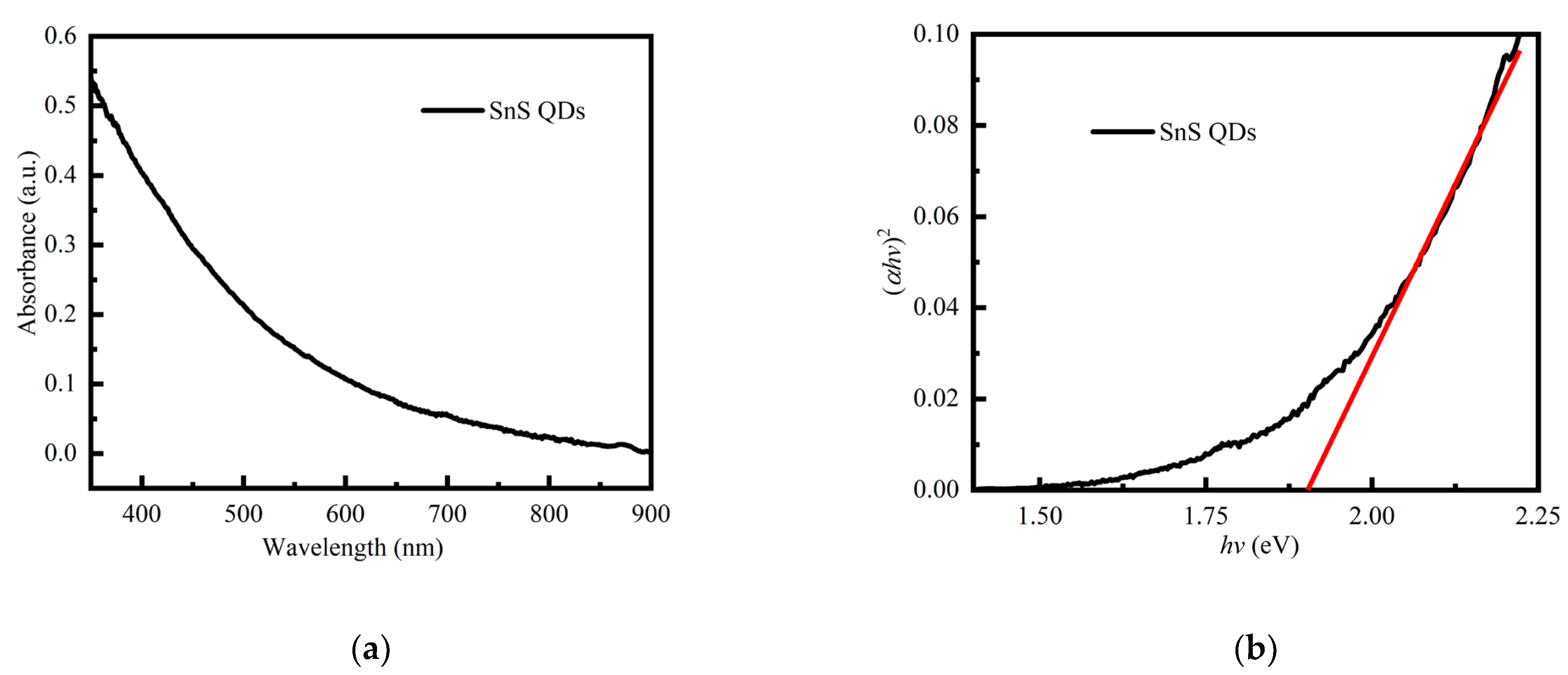
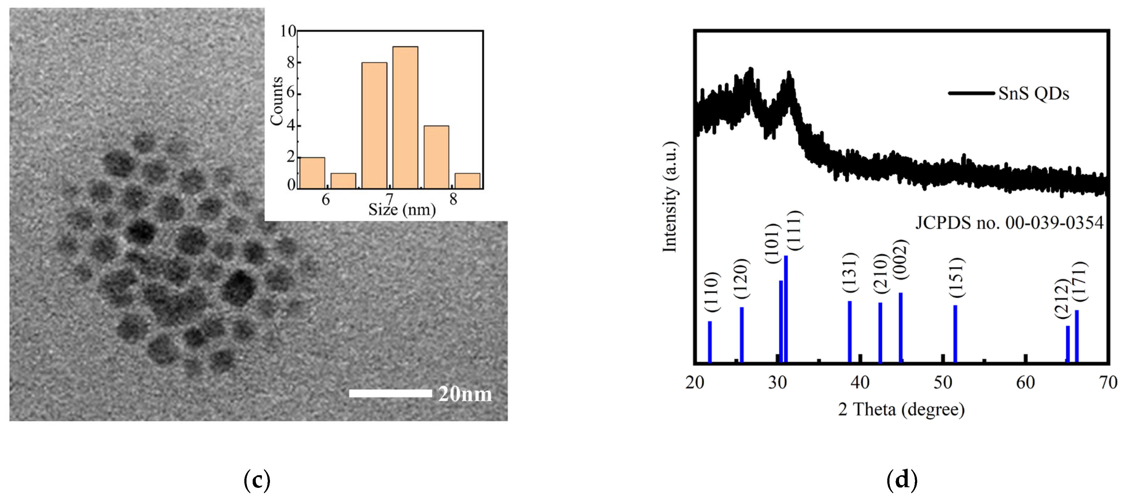
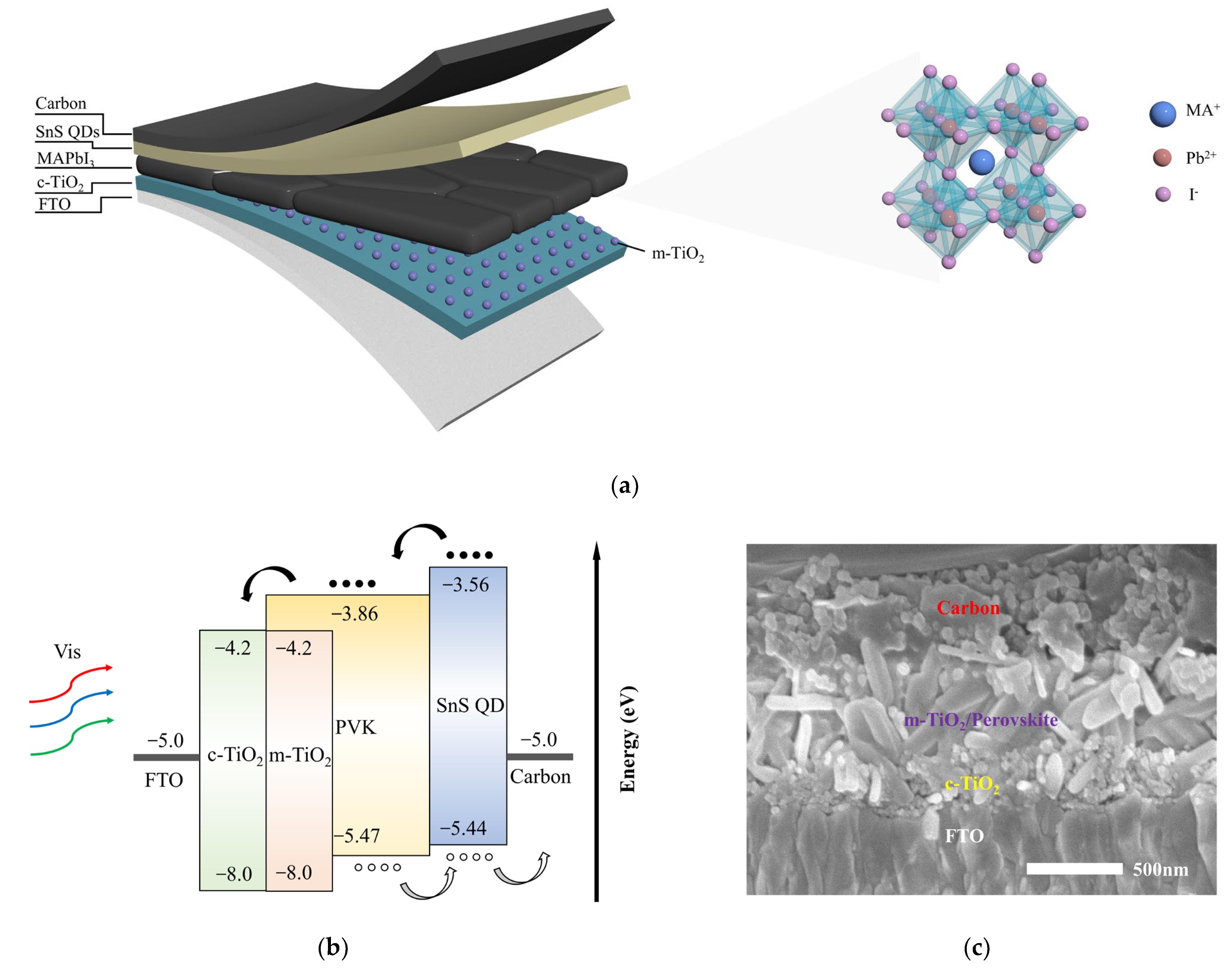
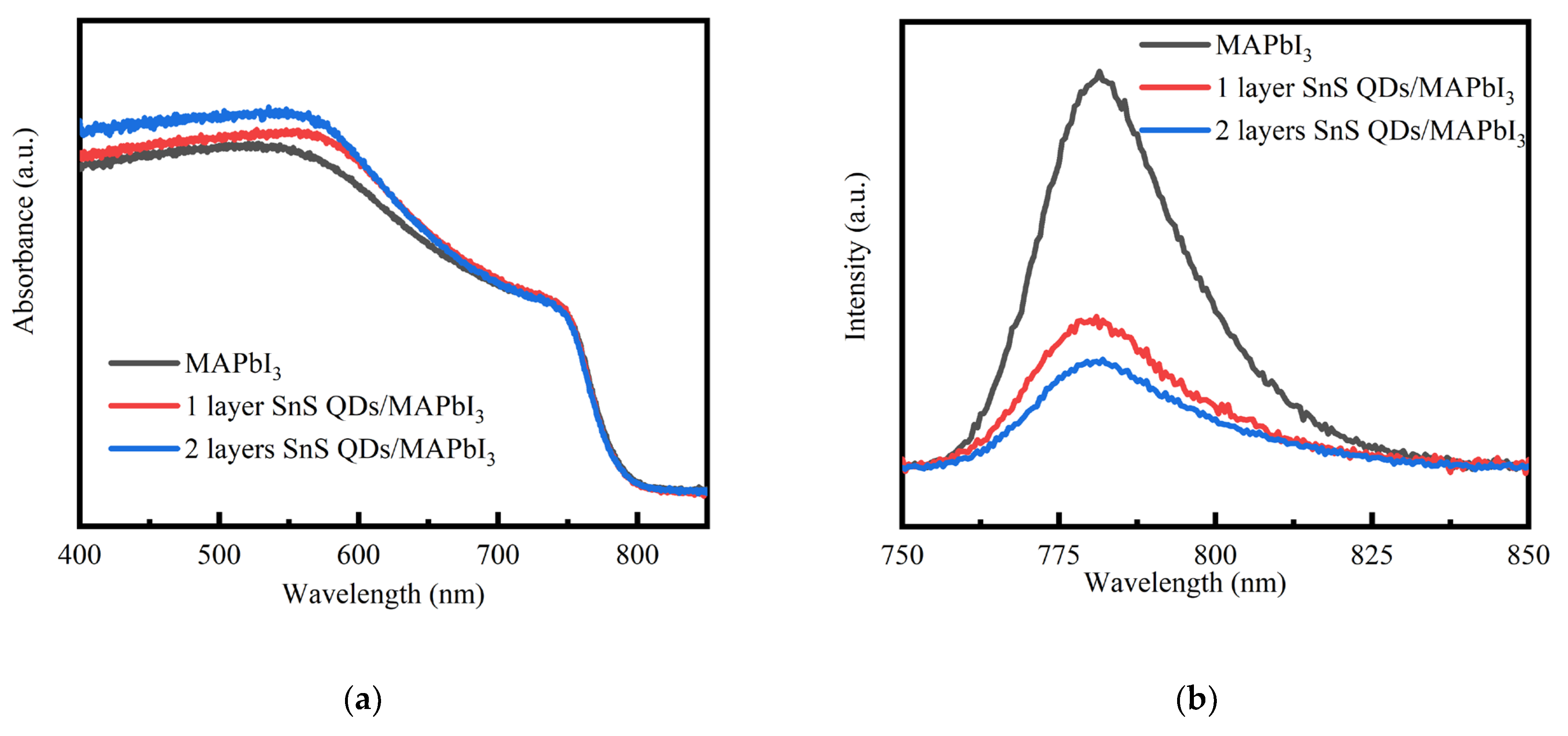
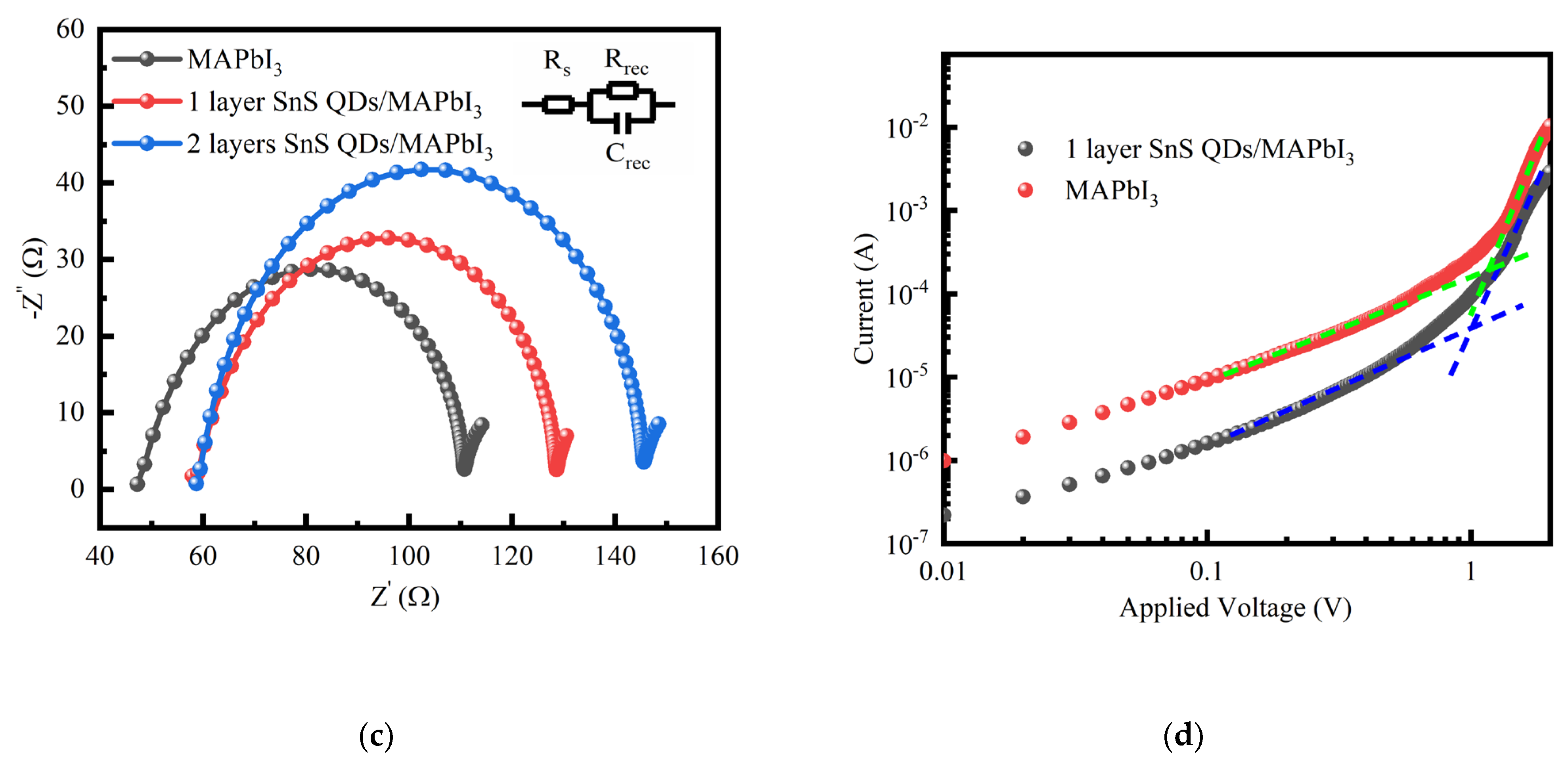
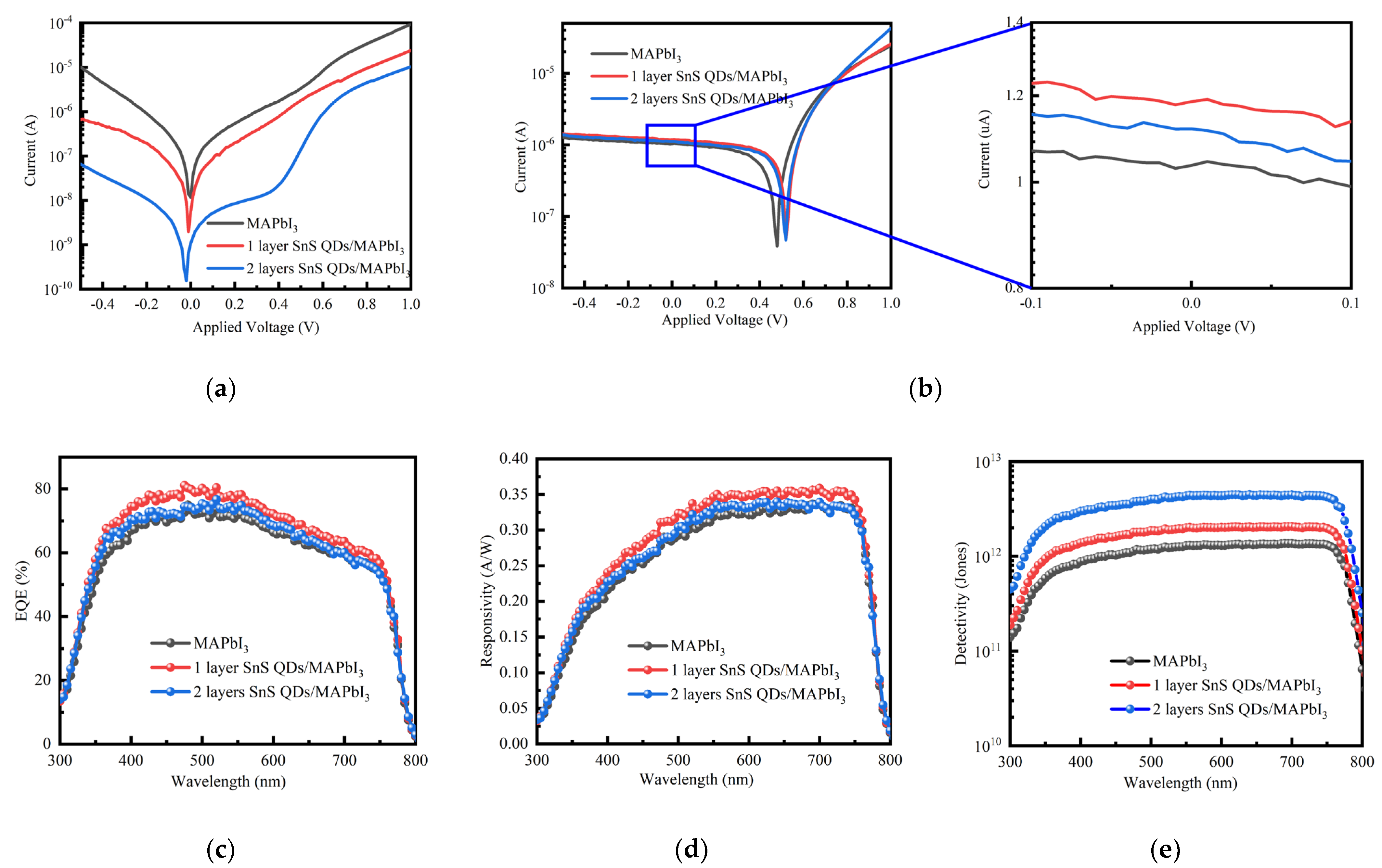
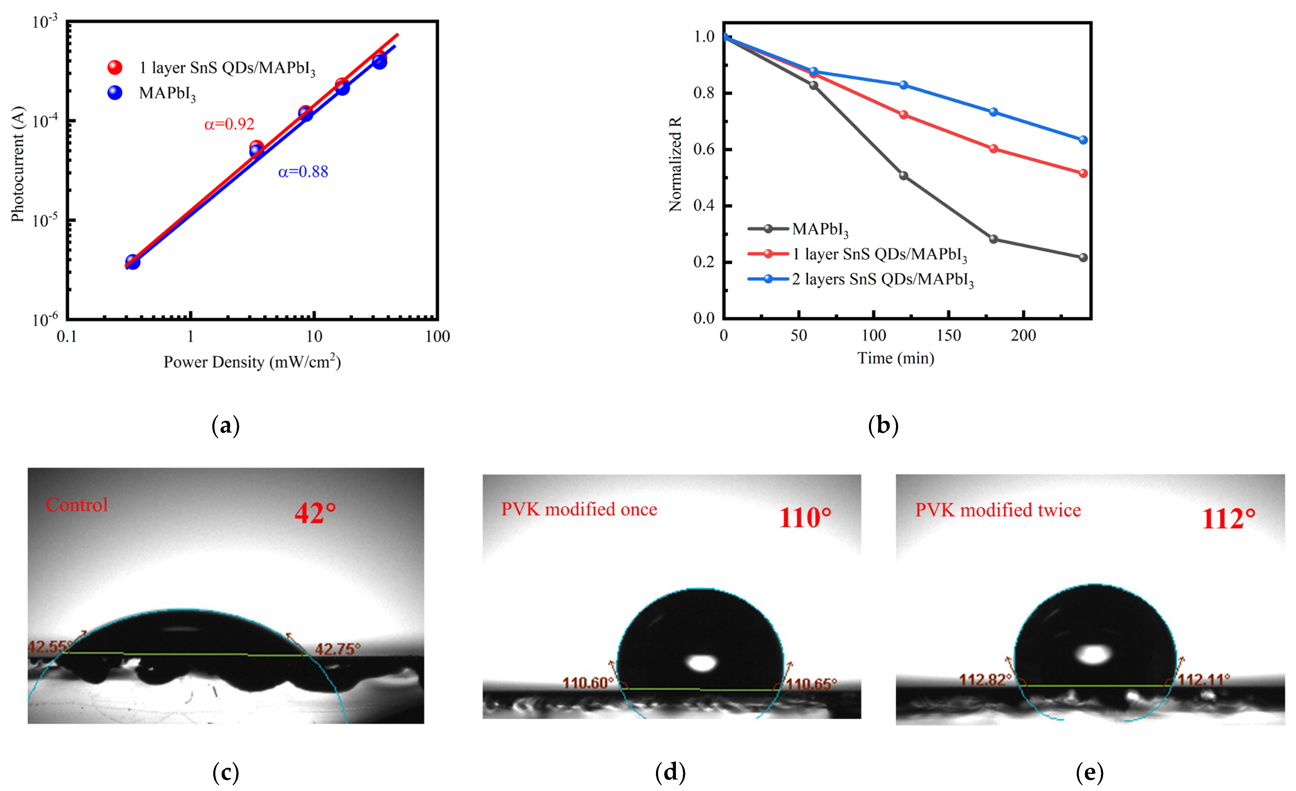
3. Results and Discussion

SnS QDs were synthesized and purified via the thermal injection method, as reported in previous literature [39]. Oleic acid (OA), oleylamine (OAm), and trioctylphosphine (TOP) were employed as capping ligands to constrain the growth of the nanoparticles. The synthesis protocol for SnS QDs is detailed in the Section 2.
The optical properties, morphology, and crystal structure of SnS QDs were characterized, with the results presented in Figure 1. Examination of Figure 1a,b reveals that the QDs demonstrate significant absorption within the visible light spectrum. The Tauc plot indicates a direct bandgap value of 1.88 eV. The TEM image shows that the QDs feature a narrow size distribution with an average diameter of 7.15 nm, as shown in Figure 1c. XRD analysis of the sample is illustrated in Figure 1d. Due to the small size of the quantum dots, the peaks are broad and weak, which makes it difficult to analyze their shape and position. However, peaks are present near the (110), (120), (101), and (111) positions of the orthorhombic phase (JCPDS no. 00-039-0354), which is a strong indication that the SnS QDs exhibit this lattice structure. In summary, our study successfully replicated synthesis and yielded high-quality SnS QDs [39,40].
Figure 2 displays the schematic representation, energy band diagram, and cross-sectional SEM image of the photodetector. The device structure comprises fluorine-doped tin oxide (FTO), compact titanium dioxide (c-TiO2), mesoporous titanium dioxide (m-TiO2), perovskite, SnS QDs, and carbon electrode. The compact TiO2 layer has a thickness of approximately 200 nm. Mesoporous TiO2 nanoparticles act as nucleation sites for facilitating their growth. In Figure 2c, TiO2 nanoparticles are embedded on the front surface of the perovskite film, with a total thickness of approximately 600 nm. Owing to the relatively low concentration of SnS QDs used in the spin-coating process, direct measurement of their thickness presented a challenge. Consequently, we estimated the thickness of the film to be ten nanometers, employing the formula for Newtonian fluids [41,42]. The energy band data were reported in our previous work [43]. The energy band diagram reveals that the addition of SnS QDs solves the band mismatch issue between perovskite and the carbon electrode. The high conduction band of SnS QDs hinders the electron migration towards the SnS QDs layer and reduces the electron–hole recombination at the back surface of the perovskite [44].
To investigate the impact of the interface layer of SnS QDs on perovskite thin film performance, a series of tests was conducted, including absorption, photoluminescence, impedance spectroscopy, and space charge limited current (SCLC) measurements. Figure 3a reveals that the quantum dot-modified composite film exhibits enhanced absorption in the visible spectrum, benefitting light collection in photodetectors. This enhancement is attributed to SnS QDs’ strong visible light absorption. SnS QDs absorb and convert the unabsorbed light of perovskite into photocurrent. Using steady-state PL analysis, we further investigated the influence of quantum dots on their ability to extract charges from perovskite layers. Figure 3b demonstrates PL reduction after device optimization. This suggests that photogenerated charge carriers are more efficiently separated and transferred to the SnS QDs layer. And the multi-layered coating yields denser interface, which can enhance the effect of hole extraction [45]. This is why the device optimized with double-layer quantum dots exhibits lower PL values. To investigate defects at the back surface of perovskite, EIS was performed in darkness at a bias voltage of 0.8 V. Figure 3c illustrates the device impedance spectra across a frequency range from 4 Mhz to 1 kHz. Under dark condition, impedance variation at high frequencies reflects the interfacial performance between the carbon electrode and the perovskite. Interface recombination resistance and series resistance were utilized to characterize these performance attributes. Interface recombination resistance mainly indicates the electron–hole recombination rate at the carbon electrode–perovskite interface, with higher interface recombination resistance suggesting enhanced charge carrier extraction efficiency and reduced recombination losses. Upon coating with QDs, there is an increase in the semicircle diameter in the high-frequency domain, corresponding to increased interface recombination resistance. Increased interface recombination resistance suggests that electron–hole recombination at the perovskite/SnS QDs interface becomes less probable, consequently favoring charge extraction.
This results from the diminished recombination centers, attributed to the QDs coordination with the perovskite surface [46]. In addition, we utilized the SCLC method to calculate the defect density, as shown in Figure 3d. The test structure consisted of FTO/PVK/carbon, and the defect density was calculated using the following formula:
N trap = 2 ε 0 ε r V TFL q L 2
Here, ε0 is the vacuum permittivity, εr is the relative permittivity, q is the elementary charge, L is the thickness of the perovskite film, and VTFL is the trap-filled limit voltage. The initial device and the device optimized with SnS QDs have VTFL values of 1.18 V and 1.01 V, respectively. After the introduction of SnS QDs, the calculated defect density Ntrap decreases from 1.03 × 1016 cm−3 to 8.83 × 1015 cm−3. This suggests that the incorporation of SnS QDs serves to passivate the surface defects in the perovskite materials, thereby reducing non-radiative recombination [47]. From a theoretical perspective, we confirmed through SCLC experiments that the decrease in defect states is not due to a decrease in the probability of radiative recombination. On this basis, the decrease in PL peak could indicate that charge carriers have been extracted into the SnS QDs layer.
Figure 4a,b illustrate the current-voltage (I-V) characteristics of the three devices both in darkness and when exposed to 500 nm wavelength illumination at an intensity of 62 µW/cm2. The increasing number of interface quantum dot modifications correlates with a decreasing trend in the dark current at 0 V bias. Specifically, the dark current measured at 0 V bias in the pristine device is 1.16 × 10⁻⁸ A; after being modified by QDs once and twice, respectively, the dark current values decrease to 5.64 × 10⁻⁹ A and 1.08 × 10⁻⁹ A, respectively. The observed reduction in dark current is attributed to the application of quantum dot coating, which serves to passivate the surface dangling bonds of the perovskite. The elimination of surface ligands and the subsequent pairing of dangling bonds on the QD surface suppress thermal excitation in the dark state, thereby reducing the dark current. Additionally, the conduction band minimum of the quantum dot layer is positioned above that of the perovskite, and this difference in energy levels serves to inhibit the reverse migration of electrons [48,49]. The reduction in dark current can be analyzed using the Shockley equation.
J dark ( V ) = J 0 [ exp ( q V / k B T ) 1 ] ,
J0 is the reverse saturation current, which is the current of the diode under reverse bias without reaching the breakdown voltage. The electron charge is q = 1.6 × 10⁻¹⁹ C, kB is the Boltzmann constant, and T is the temperature. The numerical value of J0 can be expressed by the following equation:
J 0 = q L n n 0 τ ,
τ is the minority carrier lifetime, Ln is the electron diffusion length, and n0 is the intrinsic electron concentration. When QDs passivate the back surface of perovskite, the reduction in back surface defects could lead to a decrease in the rate of minority carrier surface recombination. This may improve the surface recombination lifetime of minority carriers, thereby increasing the total lifetime of minority carriers and probably suppressing the dark current of the device.
With an increase in the number of quantum dot modifications, the device exhibits an initial increase followed by a subsequent decrease in photocurrent. The photocurrent increases from 1.03 μA to 1.18 μA and 1.12 μA after one and two quantum dot modifications, respectively. This is attributed to the concurrent absorption of visible light by both the perovskite and SnS QDs, followed by their individual transport enabled by the intrinsic electric field, resulting in enhanced harnessing of visible light. SnS QDs exist on the back surface of perovskite materials and do not affect the absorption of incident light by perovskite. SnS QDs have a high absorption coefficient, which is beneficial for them to reabsorb the unabsorbed photons of perovskite. However, the photocurrent decreases when double layers of SnS quantum dots are applied. This reduction may be attributed to an increased amount of organic ligands within the quantum dot layer as well as the induction of defects from partial ligand detachment from the quantum dot surface during the heating process. Additionally, the excessive occurrence of tin vacancies leads to an increase in defect states. Due to the further decrease in device performance after coating with more layers of quantum dots, which is consistent with the above reasons, further layer quantum dot photodetector testing was not conducted. Furthermore, quantum efficiency was performed on the three devices, evaluating their responsivity and the correlation between the spectral detectivity and the wavelength of incident light. As the wavelength increases, the external quantum efficiency (EQE) exhibits a rising trend before subsequently declining in Figure 4c. Specifically, under illumination at 500 nm, the EQE reaches approximately 80%. However, devices incorporating two layers of quantum dots exhibit decreased EQE. This can be attributed to the incorporation of additional quantum dots bound with long-chain organic ligands, which significantly impedes photocurrent transport [50]. The device featuring a single layer of QDs maintains a responsivity of approximately 0.35 A/W across the wavelength range of 550~720 nm, as shown in Figure 4d.
Additionally, throughout the visible spectrum, the device demonstrates a detection ratio of the order of 1012 (Figure 4e). In conclusion, a thorough evaluation of the device performance revealed that the single-layer quantum dot photodetector exhibits superior performance.
Significantly, the photocurrent at zero-bias voltage demonstrates a linear dependence on light power density. The photodetector linear response to light power serves as a crucial performance metric, particularly for use in light measurement and imaging applications [51]. From Figure 5, it can be seen that the basic device is no longer able to maintain a linearly increasing photocurrent under light irradiation with a power density of 0.3 mW/cm2. The device optimized by single-layer QDs is still in a linear growth state within this range. This may be because when the light intensity increases to a certain extent, the defects on the back surface of perovskite enhance the capture effect of photogenerated carriers, making it unable to maintain a linear growth trend. After quantum dot modification, defects on the back surface of perovskite are passivated, and photogenerated carriers can be effectively transported. After device optimization, the LDR exhibits an increase. Through calculation, the LDR of the device increased from 40 dB to 60 dB after QD optimization.
Similar to conventional photodetectors, the device still exhibits a saturation state when the light power is too high, and the photocurrent cannot continue to maintain a linear growth trend. To investigate the charge transfer dynamics within the detector under saturation conditions, we performed Jsc measurements as a function of light intensity. The correlation between Jsc and light intensity is described by the subsequent equation [52]:
J s c I α ( α 1 )
where α is an empirical parameter. An α value approaching 1 indicates minimal bimolecular recombination under short-circuit conditions. As depicted in Figure 6a, post optimization, the α value of the device increased from 0.88 to 0.92. This implies that, before optimization, the device exhibited considerable photogenerated charge carrier activity, trap state presence, and carrier recombination. The optimized device has improved its performance in these parts.
Compared to devices with the same structure, the photodetector in this work has higher responsivity and detectivity in Table 1. In addition, device stability is a critical factor influencing applications. Perovskite materials will quickly decompose into lead iodide when in contact with water, which will cause them to lose their photoelectric response characteristics. Conducting hydrophobic angle testing on it is an indirect method to test its water stability. As demonstrated in Figure 6c–e, by applying a coating of QDs, we successfully enhanced the device surface hydrophobicity. Following the application of single and double layers of QDs, the contact angles on the device’s surface increased to 110° and 113° from 43°, respectively. The increase in hydrophobic angle indicates that the surface of the device has a repulsive effect on water, making it difficult for water vapor to enter the interior of the device. This demonstrates that QDs modification significantly enhances the device hydrophobicity, inhibiting water decomposition reactions and improving the device wet stability. To verify its results, we conducted stability tests on it in 33 °C, 93% RH environments. From Figure 6b, it can be seen that with the increase in time, the performance of the basic device decreases the fastest. After 240 min, the optimized device still maintained 50% of its initial performance, while the performance of the basic device decreased to 20% of its initial performance. This can be attributed to the intrinsically high hydrophobicity of the SnS material, effectively decelerating water vapor diffusion, protecting the perovskite layer, and augmenting the device stability [53,54]. The hydrophobicity of SnS quantum dots may be due to capillary effects counter-balance bulk properties. Compared to optoelectronic devices optimized through P3HT, the performance degradation is almost the same (a 10% decrease in current exposed to 90% RH) [55].

4. Conclusions

In this work, we successfully fabricated SnS QDs/MAPbI3 heterojunction photodetectors. SnS QDs were deposited on the back surface of the perovskite film by employing the spin-coating technique, wherein these QDs served multiple functions: the modification of interfaces, the enhancement of light absorption, and the facilitation of hole extraction. Owing to these factors, the SnS QDs/MAPbI3 heterojunction photodetectors have high responsivity (0.32 A/W at 500 nm) and a superior detectivity (exceeding 1 × 10¹² Jones) in a self-powered mode. Compared with the pristine device, responsivity improved by 10%, and the detectivity achieved a superior standard. The findings suggest that the use of SnS QDs as an interfacial layer constitutes a promising approach to enhancing the performance of carbon-based HTL-free photodetectors. In summary, the integration of SnS QDs as an interfacial layer presents considerable potential for application within carbon-based HTL-free photodetector technology, offering an efficient means to enhance their performance.

Author Contributions

Conceptualization, Y.Y. and M.C.; methodology, Y.Y.; validation, R.Z.; formal analysis, C.S.; investigation, S.H.; resources, S.H.; data curation, S.L.; writing—original draft preparation, R.Z.; writing—review and editing, R.Z.; visualization, J.L.; supervision, M.C. All authors have read and agreed to the published version of the manuscript.

Funding

This research was funded by National Nature Science Foundation of China (22279097) and Hubei Provincial Teaching Reform Research Project (2023100).

Data Availability Statement

Data are contained within the article.

Conflicts of Interest

The authors declare no conflicts of interest.

References

  1. Koppens, F.H.; Mueller, T.; Avouris, P.; Ferrari, A.C.; Vitiello, M.S.; Polini, M. Photodetectors based on graphene, other two-dimensional materials and hybrid systems. Nat. Nanotechnol. 2014, 9, 780–793. [Google Scholar] [CrossRef]
  2. Zhang, Y.; Du, J.; Wu, X.; Zhang, G.Q.; Chu, Y.L.; Liu, D.P.; Zhao, Y.X.; Liang, Z.Q.; Jia, H. Ultrasensitive photodetectors based on island structured CH3NH3PbI3 thin films. ACS Appl. Mater. Interfaces 2015, 7, 21634–21642. [Google Scholar] [CrossRef] [PubMed]
  3. Zhang, Y.; Ma, Y.; Wang, Y.; Zhang, X.; Zuo, C.; Shen, L.; Ding, L. Lead-free perovskite photodetectors: Progress, challenges, and opportunities. Adv. Mater. 2021, 33, 2006691. [Google Scholar] [CrossRef] [PubMed]
  4. Zhang, L.; Zhou, H.; Chen, Y.; Zeng, Z.; Huang, L.; Wang, C.; Dong, K.; Hu, Z.; Ke, W.; Fang, G. Spontaneous crystallization of strongly confined CsSnxPb1-xI3 perovskite colloidal quantum dots at room temperature. Nat. Commun. 2024, 15, 1609. [Google Scholar] [CrossRef] [PubMed]
  5. Huang, Y.M.; Ma, Q.L.; Zhai, B.G. Development of porous silicon based visible light photodetectors. Key Eng. Mater. 2013, 538, 341–344. [Google Scholar] [CrossRef]
  6. Chen, Z.L.; Li, C.L.; Zhumekenov, A.A.; Zheng, X.P.; Yang, C.; Yang, H.Z.; He, Y.; Turedi, B.; Mohammed, O.F.; Shen, L.; et al. Solution-processed visible-blind ultraviolet photodetectors with nanosecond response time and high detectivity. Adv. Opt. Mater. 2019, 7, 1900506. [Google Scholar] [CrossRef]
  7. Dias, S.; Kumawat, K.L.; Krupanidhi, S.B. CH3NH3PbBr3 quantum dots for visible wavelength photodetector applications. J. Mater. Sci. Mater. Electron. 2019, 30, 3061–3068. [Google Scholar] [CrossRef]
  8. Li, G.; Wang, Y.; Huang, L.; Sun, W. Research progress of high-sensitivity perovskite photodetectors: A review of photodetectors: Noise, structure, and materials. ACS Appl. Electron. Mater. 2022, 4, 1485–1505. [Google Scholar] [CrossRef]
  9. Zhang, T.; Wang, F.; Kim, H.B.; Wang, C.F.; Cho, E.; Konefal, R.; Puttisong, Y.; Terado, K.; Gao, F. Ion-modulated radical doping of spiro-OMeTAD for more efficient and stable perovskite solar cells. Science 2022, 377, 495–501. [Google Scholar] [CrossRef]
  10. Li, X.; Zhang, W.; Guo, X.; Lu, C.; Wei, J.; Fang, J. Constructing heterojunctions by surface sulfidation for efficient inverted perovskite solar cells. Science 2022, 375, 434–437. [Google Scholar] [CrossRef]
  11. Wu, S.; Chen, R.; Zhang, S.; Babu, B.H.; Yue, Y.F.; Zhu, H.M.; Yang, Z.C.; Chen, C.L.; Chen, W.T.; Huang, Y.Q.; et al. A chemically inert bismuth interlayer enhances long-term stability of inverted perovskite solar cells. Nat. Commun. 2019, 10, 1161. [Google Scholar] [CrossRef] [PubMed]
  12. Tan, S.; Yavuz, I.; De Marco, N.; Huang, T.Y.; Lee, S.; Choi, C.S.; Wang, M.H.; Nuryyeva, S.; Wang, R.; Zhao, Y.P.; et al. Steric impediment of ion migration contributes to improved operational stability of perovskite solar cells. Adv. Mater. 2020, 32, 1906995. [Google Scholar] [CrossRef] [PubMed]
  13. Rajagopal, A.; Yao, K.; Jen, A.K.Y. Toward perovskite solar cell commercialization: A perspective and research roadmap based on interfacial engineering. Adv. Mater. 2018, 30, 1800455. [Google Scholar] [CrossRef] [PubMed]
  14. Ku, Z.; Rong, Y.; Xu, M.; Liu, T.; Han, H. Full printable processed mesoscopic CH3NH3PbI3/TiO2 heterojunction solar cells with carbon counter electrode. Sci. Rep. 2013, 3, 3132. [Google Scholar] [CrossRef] [PubMed]
  15. Sheng, Y.; Mei, A.; Liu, S.; Duan, M.; Jiang, P.; Tian, C.B.; Ong, Y.; Rong, Y.G.; Han, H.W.; Hu, T. Mixed (5-AVA)xMA1−xPbI3−y(BF4)y perovskites enhance the photovoltaic performance of hole- conductor-free printable mesoscopic solar cells. J. Mater. Chem. A 2018, 6, 2360–2364. [Google Scholar] [CrossRef]
  16. Xiong, Y.; Liu, Y.; Lan, K.; Mei, A.; Sheng, Y.; Zhao, D.; Han, H. Fully printable hole-conductor-free mesoscopic perovskite solar cells based on mesoporous anatase single crystals. New J. Chem. 2018, 42, 2669–2674. [Google Scholar] [CrossRef]
  17. You, S.; Wang, H.; Bi, S.Q.; Zhou, J.Y.; Qin, L.; Qiu, X.H.; Zhao, Z.Q.; Xu, Y.; Zhang, Y.; Shi, X.H.; et al. A Biopolymer Heparin Sodium Interlayer Anchoring TiO2 and MAPbI3 Enhances Trap Passivation and Device Stability in Perovskite Solar Cells. Adv. Mater. 2018, 30, 1706924. [Google Scholar] [CrossRef] [PubMed]
  18. Li, Y.Q.; Lu, X.Y.; Mei, Y.T.; Dong, C.; Gangadharan, D.T.; Liu, K.; Wang, Z.J.; Qu, S.C.; Saidaminov, M.I.; Zhang, W.F. Blade-coated carbon electrode perovskite solar cells to exceed 20% efficiency through protective buffer layers. Adv. Funct. Mater. 2023, 33, 2301920. [Google Scholar] [CrossRef]
  19. Chen, K.; Xiao, X.F.; Liu, J.L.; Qi, J.H.; Gao, Q.J.; Ma, Y.M.; Cheng, Y.J.; Mei, A.Y.; Han, H.W. Record-efficiency printable hole-conductor-free mesoscopic perovskite solar cells enabled by the multifunctional schiff base derivative. Adv. Mater. 2024, 3, 2401319. [Google Scholar] [CrossRef]
  20. Binyamin, T.; Etgar, L. Ways to improve the performance of triple-mesoscopic hole-conductor-free perovskite-based solar cells. Sol. RRL 2022, 6, 2200295. [Google Scholar] [CrossRef]
  21. Wang, D.; Chen, Q.; Mo, H.; Cheng, D.; Liu, X.; Liu, W.; Jacobs, J.; Thomas, A.G.; Liu, Z.; Curry, R.J. In situ laser generation of NiOx nanoparticles embedded in graphene flakes for ambient-processed hole-transport-layer-free perovskite solar cells. Carbon 2023, 214, 118360–118370. [Google Scholar] [CrossRef]
  22. Wang, Y.; Li, L.; Wu, Z.; Zhang, R.; Hong, J.; Zhang, J.; Rao, H.; Pan, Z.; Zhong, X. Self-driven prenucleation-induced perovskite crystallization enables efficient perovskite solar cells. Angew. Chem. Int. Ed. 2023, 62, 202302342. [Google Scholar] [CrossRef] [PubMed]
  23. Qian, J.; Yong, K.T.; Roy, I.; Ohulchanskyy, T.Y.; Bergey, E.J.; Lee, H.H.; Tramposch, K.M.; He, S.L.; Maitra, A.; Prasad, P.N. Imaging pancreatic cancer using surface-functionalized quantum dots. J. Phys. Chem. B 2007, 111, 6969–6972. [Google Scholar] [CrossRef] [PubMed]
  24. Jeong, D.W.; Kim, J.Y.; Seo, H.W.; Lim, K.M.; Ko, M.J.; Seong, T.Y.; Kim, B.S. Characteristics of gradient-interface-structured ZnCdSSe quantum dots with modified interface and its application to quantum-dot-sensitized solar cells. Appl. Surf. Sci. 2018, 429, 16–22. [Google Scholar] [CrossRef]
  25. Yang, Y.; Wang, S.; Li, S.; Li, T.; Chen, P.; Zhao, Q.; Li, G. Quantum dot bridges enabling highly efficient carbon-based hole transport material-free perovskite solar cells. Sol. RRL 2023, 7, 2300606. [Google Scholar] [CrossRef]
  26. Zhou, H.P.; Chen, M.W.; Liu, C.G.; Zhang, R.; Li, J.; Liao, S.N.; Lu, H.F.; Yang, Y.P. Interfacial passivation of CsPbI3 quantum dots improves the performance of hole-transport-layer-free perovskite photodetectors. Discover Nano 2023, 18, 11. [Google Scholar] [CrossRef] [PubMed]
  27. Vijayaraghavan, S.N.; Wall, J.; Li, L.; Xiong, G.; Zhang, Q.; Yan, F. Low-temperature processed highly efficient hole transport layer free carbon-based planar perovskite solar cells with SnO2 quantum dot electron transport layer. Mater. Today Phys. 2020, 13, 100204. [Google Scholar] [CrossRef]
  28. Qi, X.; Wang, J.; Tan, F.; Dong, C.; Liu, K.; Li, X.; Zhang, L.; Wu, H.; Wang, H.L.; Qu, S.; et al. Quantum dot interface-mediated CsPbIBr2 film growth and passivation for efficient carbon-based solar cells. ACS Appl. Mater. Interfaces 2021, 13, 55349–55357. [Google Scholar] [CrossRef] [PubMed]
  29. Sui, H.; He, B.; Ti, J.; Sun, S.; Jiao, W.; Chen, H.; Duan, Y.; Yang, P.; Tang, Q. Sulfur vacancy defects healing of WS2 quantum dots boosted hole extraction for all-inorganic perovskite solar cells. Chem. Eng. J. 2023, 455, 140728. [Google Scholar] [CrossRef]
  30. Xu, Y.; Al-Salim, N.; Bumby, C.W.; Tilley, R.D. Synthesis of SnS Quantum Dots. J. Am. Chem. Soc. 2009, 131, 15990–15999. [Google Scholar] [CrossRef]
  31. Wang, Y.H.; Chen, Z.; Zhou, X.Q. Synthesis and photoluminescence of ZnS quantum dots. Nanosci. Nanotechnol. Lett. 2008, 8, 1312–1315. [Google Scholar]
  32. Li, Y.; Wang, Z.W.; Ren, D.; Liu, Y.; Zheng, A.; Zakeeruddin, S.M.; Dong, X.; Hagfeldt, A.; Gratzel, M. SnS quantum dots as hole transporter of perovskite solar cells. ACS Appl. Electron. Mater. 2019, 2, 3822–3829. [Google Scholar] [CrossRef]
  33. Rath, J.K.; Prastani, C.; Nanu, D.E.; Nanu, N.; Schropp, R.; Vetushka, A.; Hyvl, M.; Fejfar, A. Fabrication of SnS quantum dots for solar-cell applications: Issues of capping and doping. Phys. Status Solidi B 2014, 251, 1309–1321. [Google Scholar] [CrossRef]
  34. Zhou, H.; Yang, L.; Gui, P.B.; Grice, C.R.; Song, Z.H.; Wang, H.; Fang, G.J. Ga-doped ZnO nanorod scaffold for high-performance, hole-transport-layer free, self-powered CH3NH3PbI3 perovskite photodetectors. Sol. Energy Mater. Sol. Cells 2019, 193, 246–252. [Google Scholar] [CrossRef]
  35. Zhang, T.; Ren, Z.Y.; Guo, S.Y.; Zhang, G.J.; Wang, S.F.; Qiao, S. Broadband Self-Powered CdS ETL-Based MAPbI3 Heterojunction Photodetector Induced by a Photovoltaic−Pyroelectric−Thermoelectric Effect. ACS Appl. Mater. Interfaces 2023, 15, 44444–44455. [Google Scholar] [CrossRef] [PubMed]
  36. Liu, Z.Y.; Liu, X.Y.; Sun, B.; Tan, X.H.; Ye, H.B.; Zhou, J.X.; Tang, Z.R.; Shi, T.L.; Liao, G.L. A Cu-doping strategy to enhance photoelectric performance of self-powered hole-conductor-free perovskite photodetector for optical communication applications. Adv. Mater. Technol. 2020, 5, 2000260. [Google Scholar] [CrossRef]
  37. Li, Z.B.; Li, H.N.; Jiang, K.; Ding, D.; Li, J.N.; Ma, C.; Jiang, S.C.; Wang, Y.; Anthopoulos, T.D.; Shi, Y.M. Self-powered perovskite/CdS heterostructure photodetectors. ACS Appl. Mater. Interfaces 2019, 11, 40204–40213. [Google Scholar] [CrossRef] [PubMed]
  38. Murali, S.; Madhusudanan, S.; Pathak, A.; Jayasankar, P.M.; Batabyal, S.K. Carbon assisted methylammonium lead iodide microcrystalline device for an inexpensive self-powered photodetector. Mater. Lett. 2019, 254, 428–432. [Google Scholar] [CrossRef]
  39. Luo, X.H.; He, Z.Y.; Meng, R.W.; Zhang, C.; Chen, M.; Lu, H.; Yang, Y. SnS quantum dots with different sizes in active layer for enhancing the performance of perovskite solar cells. Appl. Phys. A 2021, 127, 8396–8417. [Google Scholar] [CrossRef]
  40. Burton, L.A.; Walsh, A. Phase stability of the earth-abundant tin sulfides SnS, SnS2, and Sn2S3. J. Phys. Chem. C 2012, 116, 24262. [Google Scholar] [CrossRef]
  41. Lee, U.G.; Kim, W.B.; Han, D.H.; Chung, H.S. A modified equation for thickness of the film fabricated by spin coating. Symmetry 2019, 11, 1183. [Google Scholar] [CrossRef]
  42. Emslie, A.G.; Bonner, F.T.; Peck, L.G. Flow of a viscous liquid on a rotating disk. J. Appl. Phys. 1958, 29, 858–862. [Google Scholar] [CrossRef]
  43. Luo, X.H. Study on the Effect of SnS Quantum Dots Doped Active Layer on the Photovoltaic Performance of Photovoltaic Cells. Master’s Thesis, Wuhan University of Technology, Wuhan, China, 2021. [Google Scholar]
  44. Shin, D.H.; Shin, S.H.; Lee, S.G.; Kim, S.; Choi, S.H. High-detectivity/-speed flexible and self-powered graphene quantum dots/perovskite photodiodes. ACS Sustain. Chem. Eng. 2019, 7, 19961–19968. [Google Scholar] [CrossRef]
  45. Rakstys, K.; Abate, A.; Dar, M.I.; Gao, P.; Jankauskas, V.; Jacopin, G.; Kamarauskas, E.; Kazim, S.; Ahmad, S.; Gratzel, M.; et al. Triazatruxene-based hole transporting materials for highly efficient perovskite solar cells. J. Am. Chem. Soc. 2015, 137, 16172–16178. [Google Scholar] [CrossRef] [PubMed]
  46. Hu, S.; Duan, C.; Du, H.; Zeng, S.; Kong, A.; Chen, Y.; Peng, Y.; Cheng, Y.B.; Ku, Z. A stress relaxation strategy for preparing high-quality organic–inorganic perovskite thin films via a vapor–solid reaction. J. Mater. Chem. A 2023, 11, 23387–23396. [Google Scholar] [CrossRef]
  47. Gao, Z.W.; Wang, Y.; Choy, W.C.H. Buried Interface Modification in Perovskite Solar Cells: A Materials Perspective. Adv. Energy Mater. 2022, 12, 2104030. [Google Scholar] [CrossRef]
  48. Park, Y.D.; Lim, J.A.; Lee, H.S.; Cho, K. Interface engineering in organic transistors. Mater. Today 2007, 10, 46–54. [Google Scholar] [CrossRef]
  49. Ravi, V.K.; Markad, G.B.; Nag, A. Band edge energies and excitonic transition probabilities of colloidal CsPbX3 (X = Cl, Br, I) perovskite nanocrystals. ACS Energy Lett. 2016, 1, 665–671. [Google Scholar] [CrossRef]
  50. Zhang, J.Y.; Xu, J.L.; Chen, T.; Gao, X.; Wang, S.D. Toward broadband imaging: Surface-engineered PbS quantum dot/perovskite composite integrated ultrasensitive photodetectors. ACS Appl. Mater. Interfaces 2019, 11, 44430–44437. [Google Scholar] [CrossRef]
  51. Bao, C.; Yang, J.; Bai, S.; Xu, W.; Yan, Z.; Xu, Q.; Liu, J.; Zhang, W.; Gao, F. High performance and stable all-inorganic metal halide perovskite-based photodetectors for optical communication applications. Adv. Mater. 2018, 30, 1803422. [Google Scholar] [CrossRef]
  52. Sulaman, M.; Yang, S.; Bukhtiar, A.; Tang, P.Y.; Zhang, Z.H.; Song, Y.; Imran, A.; Jiang, Y.R.; Cui, Y.Y.; Tang, L.B.; et al. Hybrid bulk-heterojunction of colloidal quantum dots and mixed-halide perovskite nanocrystals for high performance self-powered broadband photodetectors. Adv. Funct. 2022, 32, 2201527. [Google Scholar] [CrossRef]
  53. Poli, I.; Liang, X.; Baker, R.; Eslava, S.; Cameron, P. Enhancing the hydrophobicity of perovskite solar cells using C18 capped CH3NH3PbI3 nanocrystals. J. Phys. Chem. C 2018, 6, 7149–7156. [Google Scholar] [CrossRef]
  54. Spalatu, N.; Hiie, J.; Kaupmees, R.; Volobujeva, O.; Krustok, J.; Acik, I.O.; Krunks, M. Postdeposition processing of SnS thin films and solar cells: Prospective strategy to obtain large, sintered, and doped SnS grains by recrystallization in the presence of a metal halide flux. ACS Appl. Mater. Interfaces 2019, 11, 17539–17554. [Google Scholar] [CrossRef] [PubMed]
  55. Xiong, J.; Qi, Y.; Zhang, Q.; Box, D.; Williams, K.; Tatum, J.; Das, P.; Ranjan, N.; Dai, Q. Enhanced Moisture and Water Resistance in Inverted Perovskite Solar Cells by Poly(3-hexylthiophene). ACS Appl. Energy Mater. 2021, 4, 1815–1823. [Google Scholar] [CrossRef]
  56. Ghosh, J.; Natu, G.; Giri, P.K. Plasmonic hole-transport-layer enabled self-powered hybrid perovskite photodetector using a modifed perovskite deposition method in ambient air. Org. Electron. 2019, 71, 175–184. [Google Scholar] [CrossRef]
  57. Yeddu, V.; Seo, G.; Bamidele, M.; Jung, H.; Yu, H.; Lee, J.W.; Lee, J.; Kim, D.Y. High-detectivity UV−VIS−NIR broadband perovskite photodetector using a mixed Pb−Sn narrow-band-gap absorber and a NiOx electron blocker. ACS Appl. Electron. Mater. 2022, 4, 1206–1213. [Google Scholar] [CrossRef]
  58. He, Z.; Yang, Y.; Liu, J.; Li, J.; Lu, X.; Zou, J.; Yang, S.; Zou, Y. Antisolvent-treated MAPbI3 and PbS quantum dots for high performance broadband photodetectors. ACS Appl. Nano Mater. 2023, 6, 1119–1128. [Google Scholar] [CrossRef]
  59. Huang, H.; Zhao, C.; Zhang, X.; Wang, K.; Fu, J.; Guo, J.; Wang, S.; Zhao, Q.; Ma, W.; Yuan, J. Controllable colloidal synthesis of MAPbI3 perovskite nanocrystals for dual-mode optoelectronic applications. Nano Lett. 2023, 23, 9143–9150. [Google Scholar] [CrossRef]
Figure 1. (a) UV–vis absorption spectra, (b) Tauc plot and fitting line, (c) TEM images, and (d) XRD patterns of as-synthesized SnS QDs. The inset of (c) shows size histogram of SnS QDs.
Nanomaterials 14 00956 g001aNanomaterials 14 00956 g001b
Figure 2. (a) Device structure, (b) band alignment, and (c) cross-sectional SEM of fabricated carbon-based HTM-free photodetector modified with SnS QDs once.
Nanomaterials 14 00956 g002
Figure 3. (a) UV-vis absorption; (b) steady-state PL spectra of the perovskite films modified with SnS QDs for various times; (c) EIS data and (d) SCLC curves for the pristine and SnS QDs-modified devices and fitting line. The inset of (c) shows the simplified equivalent circuit for the impedance spectroscopy analysis.
Nanomaterials 14 00956 g003aNanomaterials 14 00956 g003b
Figure 4. (a) Dark I-V curves and (b) light I-V curves of different devices. A magnified view of (b) is shown for distinguishing the differences in photocurrent of three devices under 0 V bias. (c) External quantum efficiency (EQE), (d) spectral responsivity, and (e) spectral detectivity of the pristine and SnS QDs-modified devices.
Nanomaterials 14 00956 g004
Figure 5. The photocurrent vs. voltage of (a) basic devices and (b) single-layer QDs optimized devices under 500 nm light irradiation. (c) The photocurrent vs. power density of basic devices and single-layer QDs under 500 nm light irradiation.
Nanomaterials 14 00956 g005
Figure 6. (a) Light intensity-dependent photocurrent curves of the pristine and device modified with SnS QDs once. (b) Stability testing of three devices. Water contact angle images of the (c) perovskite film and the SnS QDs films deposited on the perovskite substrate (d) once and (e) twice.
Nanomaterials 14 00956 g006
Table 1. Summary of performance parameters and device structure of photodetectors.
Device StructureR(A/W) 500 nmD* (Jones)τrisefallRef.
FTO/PEDOT: PSS + Ag NPs/MAPbI3/Al0.251.5 × 1011110 ms/72 ms[56]
ITO/NiOx/Pb-Sn Perovskite/C60/TmPyPB/Ag0.32>1 × 101214 μs/14 μs[57]
ITO/NiOx/PbS QDs/MAPbI3/PC61BM/Ag0.345.6 × 10113.5 μs/35 μs[58]
FTO/TiO2/MAPbI3 PNCs/PTAA/MoO3/Ag0.272 × 101146 ms/47 ms[59]
FTO/TiO2/m-TiO2/MAPbI3/SnS QDs/Carbon0.321.9 × 101247 ms/43 msThis work
Disclaimer/Publisher’s Note: The statements, opinions and data contained in all publications are solely those of the individual author(s) and contributor(s) and not of MDPI and/or the editor(s). MDPI and/or the editor(s) disclaim responsibility for any injury to people or property resulting from any ideas, methods, instructions or products referred to in the content.

