
Optimization of Electrospray Deposition Conditions of ZnO Thin Films for Ammonia Sensing

 , ,
, , 
Abstract
1. Introduction
2. Materials and Methods
2.1. Deposition of ZnO Thin Films
2.2. Study of Films’ Properties
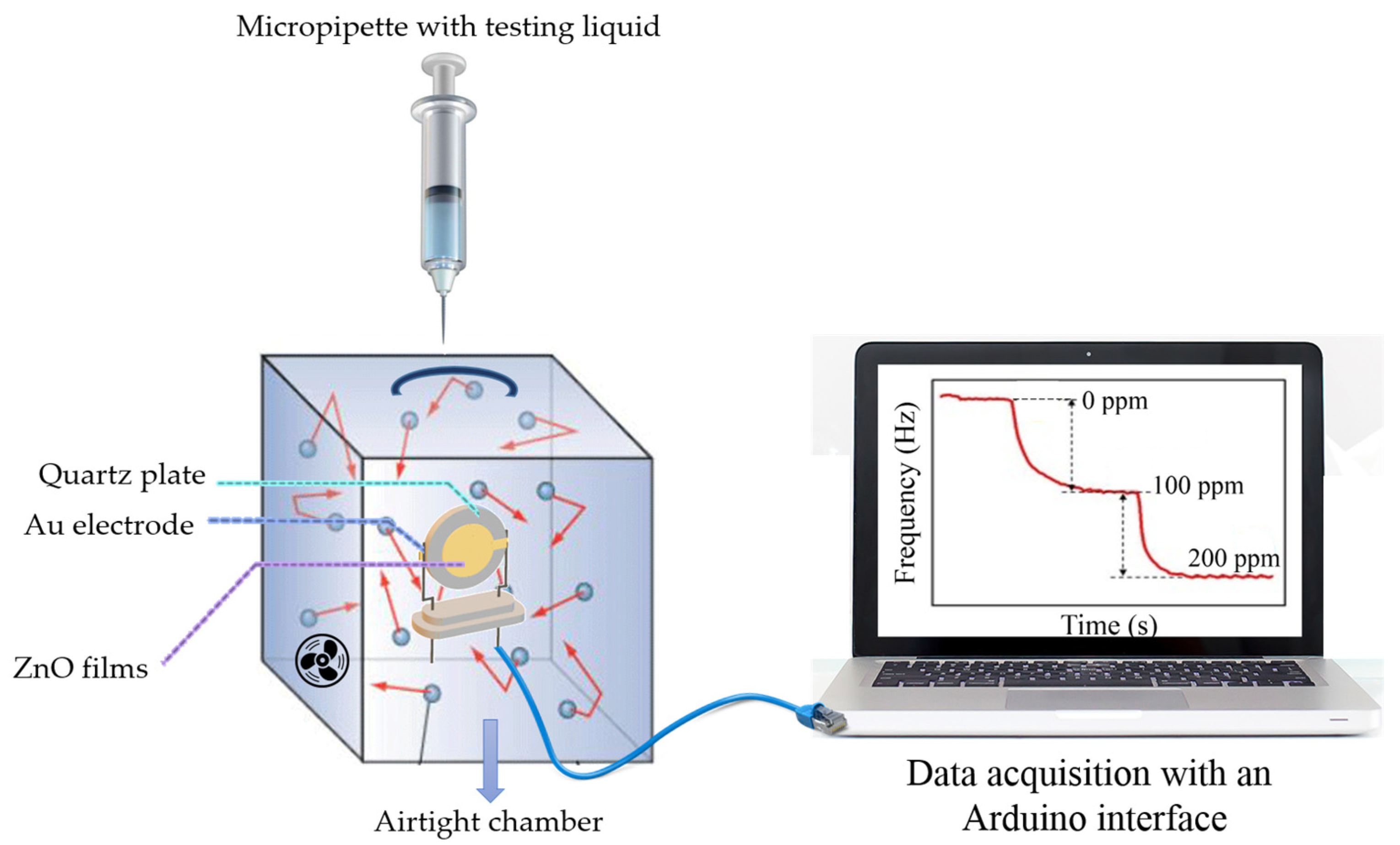
2.3. Study of Gas Sensing Properties
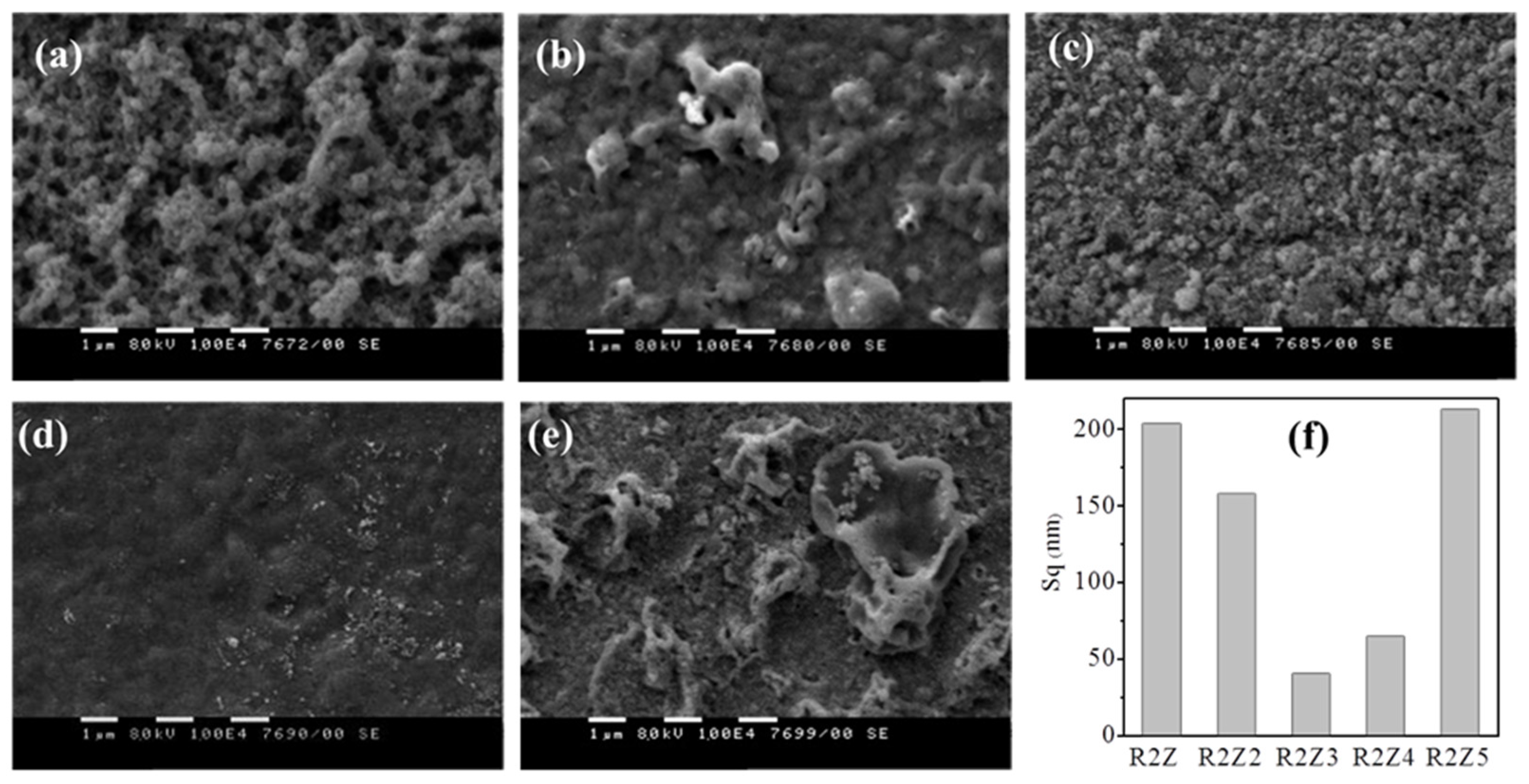
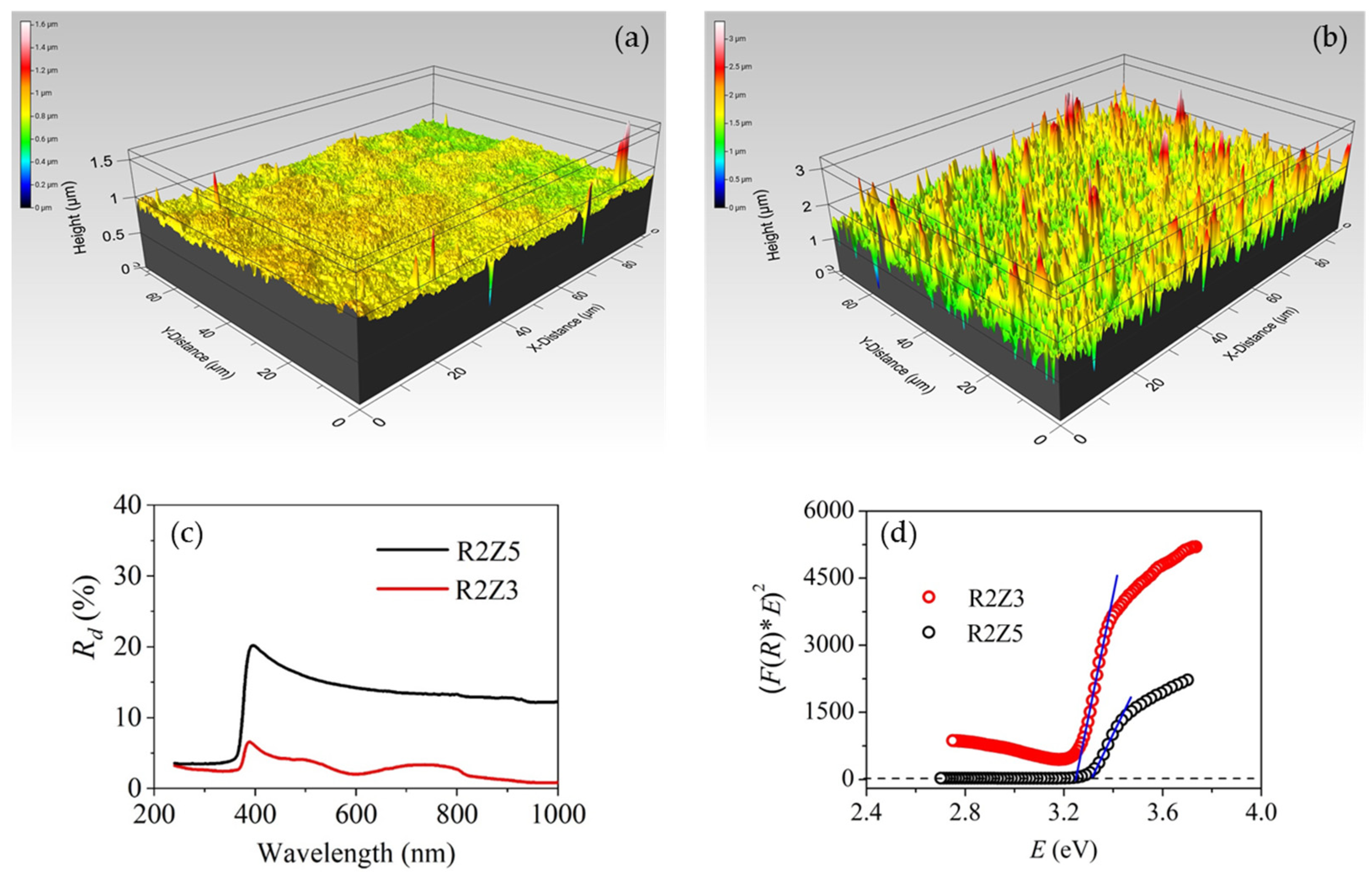
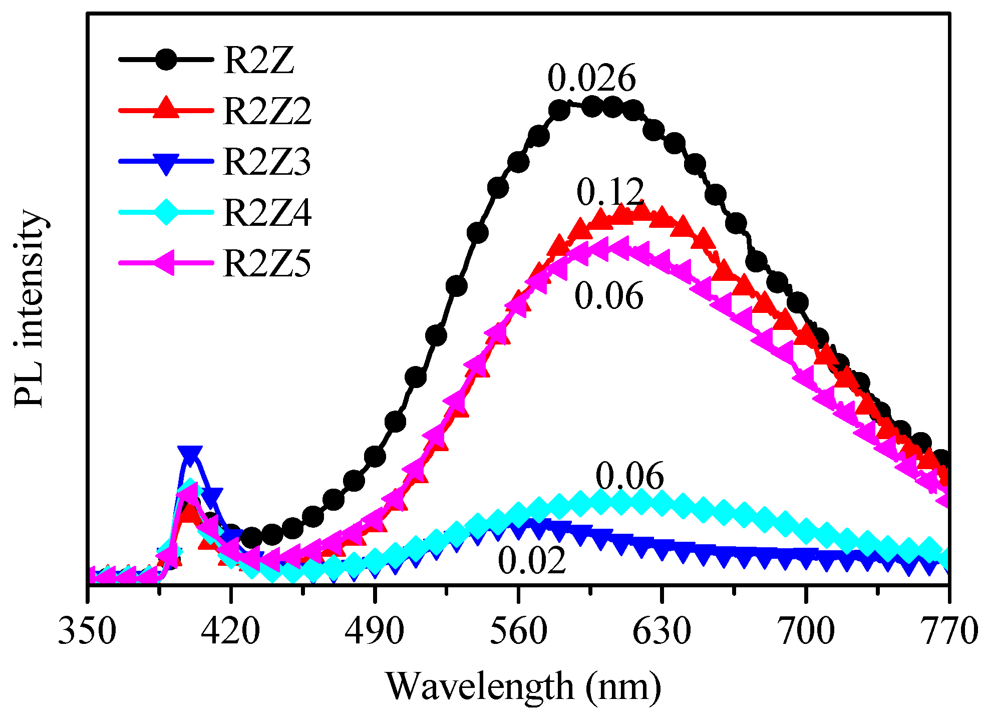
3. Results and Discussion
4. Conclusions
Author Contributions
Funding
Data Availability Statement
Acknowledgments
Conflicts of Interest
References
- Saruhan, B.; Fomekong, R.L.; Nahirniak, S. Review: Influences of semiconductor metal oxide properties on gas sensing characteristics. Front. Sens. 2021, 2, 657931. [Google Scholar] [CrossRef]
- Ganesh, S.R.; Durgadevi, E.; Navaneethan, M.; Patil, V.L.; Ponnusamy, S.; Muthamizhchelvan, C.; Kawasaki, S.; Patil, P.S.; Hayakawa, Y. Tuning the selectivity of NH3 gas sensing response using Cu-doped ZnO nanostructures. Sens. Actuators A 2018, 269, 331–341. [Google Scholar] [CrossRef]
- Wei, A.; Pan, L.; Huang, W. Recent progress in the ZnO nanostructure-based sensors. Mater. Sci. Eng. B 2011, 176, 1409–1421. [Google Scholar] [CrossRef]
- Alvi, N.H.; Mulla, M.Y.; Abitbol, T.; Fall, A.; Beni, V. The Fast and One-Step Growth of ZnO Nanorods on Cellulose Nanofibers for Highly Sensitive Photosensors. Nanomaterials 2023, 13, 2611. [Google Scholar] [CrossRef]
- Pachauri, V.; Vlandas, A.; Kern, K.; Balasubramanian, K. Site-Specific Self-Assembled Liquid-Gated ZnO Nanowire Transistors for Sensing Applications. Small 2010, 6, 589–594. [Google Scholar] [CrossRef]
- Fang, X.; Bando, Y.; Gautam, U.K.; Zhai, T.; Zeng, H.; Xu, X.; Liao, M.; Golberg, D. ZnO and ZnS Nanostructures: Ultraviolet-Light Emitters, Lasers, and Sensors. Crit. Rev. Solid State Mater. Sci. 2009, 34, 190–223. [Google Scholar] [CrossRef]
- Zhang, Q.F.; Dandeneau, C.S.; Zhou, X.Y.; Cao, G.Z. ZnO Nanostructures for Dye-Sensitized Solar Cells. Adv. Mater. 2009, 21, 4087–4108. [Google Scholar] [CrossRef]
- Semong, O.; Batlokwa, B.S. Rapid Colorimetric Detection of Hg (II) Based on Hg (II)-Induced Suppressed Enzyme-Like Reduction of 4-Nitrophenol by Au@ ZnO/Fe3O4 in a Cosmetic Skin Product. Nanomater. Nanotechnol. 2023, 2023, 3603680. [Google Scholar] [CrossRef]
- Dimitrov, D.; Tsai, C.-L.; Petrov, S.; Marinova, V.; Petrova, D.; Napoleonov, B.; Blagoev, B.; Strijkova, V.; Hsu, K.Y.; Lin, S.H. Atomic layer-deposited Al-doped ZnO thin films for display applications. Coatings 2020, 10, 539. [Google Scholar] [CrossRef]
- Chang, Y.; Yang, W.; Chang, C.; Hsu, P.; Chen, L. Controlled Growth of ZnO Nanopagoda Arrays with Varied Lamination and Apex Angles. Cryst. Growth Des. 2009, 9, 3161–3167. [Google Scholar] [CrossRef]
- Cho, S.; Jung, S.; Lee, K. Morphology-Controlled Growth of ZnO Nanostructures Using Microwave Irradiation: From Basic to Complex Structures. J. Phys. Chem. C 2008, 112, 12769–12776. [Google Scholar] [CrossRef]
- Ramike, M.P.; Ndungu, P.G.; Mamo, M.A. Exploration of the Different Dimensions of Wurtzite ZnO Structure Nanomaterials as Gas Sensors at Room Temperature. Nanomaterials 2023, 13, 2810. [Google Scholar] [CrossRef]
- Mazeina, L.; Picard, S.Y.N.; Prokes, M. Controlled Growth of Parallel Oriented ZnO Nanostructural Arrays on Ga2O3 Nanowires. Cryst. Growth Des. 2009, 9, 1164–1169. [Google Scholar] [CrossRef]
- Ram, S.D.G.; Ravi, G.; Athimoolam, A.; Mahalingam, T.; Kulandainathan, A. Aqueous chemical growth of free standing vertical ZnO nanoprisms, nanorods and nanodiskettes with improved texture co-efficient and tunable size uniformity. Appl. Phys. A 2011, 105, 881–890. [Google Scholar] [CrossRef]
- Shen, G.; Bando, Y.; Lee, C. Synthesis and Evolution of Novel Hollow ZnO Urchins by a Simple Thermal Evaporation Process. J. Phys. Chem. B 2005, 109, 10578–10583. [Google Scholar] [CrossRef]
- Deng, H.; Russell, J.J.; Lamb, R.N.; Jiang, B.; Li, Y.; Zhou, X.Y. Microstructure control of ZnO thin films prepared by single source chemical vapor deposition. Thin Solid Film. 2004, 458, 43–46. [Google Scholar] [CrossRef]
- Zhang, B.P.; Binh, N.T.; Segawa, Y.; Wakatsuki, K.; Usami, N. Optical properties of ZnO rods formed by metalorganic chemical vapor deposition. Appl. Phys. Lett. 2003, 83, 1635–1637. [Google Scholar] [CrossRef]
- Karajz, D.A.; Szilágyi, I.M. Review of photocatalytic ZnO nanomaterials made by atomic layer deposition. Surf. Interfaces 2023, 40, 103094. [Google Scholar] [CrossRef]
- Dimitrov, D.Z.; Chen, Z.F.; Marinova, V.; Petrova, D.; Ho, C.Y.; Napoleonov, B.; Blagoev, B.; Strijkova, V.; Hsu, K.Y.; Lin, S.H.; et al. ALD Deposited ZnO:Al Films on Mica for Flexible PDLC Devices. Nanomaterials 2021, 11, 1011. [Google Scholar] [CrossRef] [PubMed]
- Huby, N.; Ferrari, S.; Guziewicz, E.; Godlewski, M.; Osinniy, V. Electrical behavior of zinc oxide layers grown by low temperature atomic layer deposition. Appl. Phys. Lett. 2008, 92, 023502. [Google Scholar] [CrossRef]
- Park, K.C.; Ma, D.Y.; Kim, K.H. The physical properties of Al-doped zinc oxide films prepared by RF magnetron sputtering. Thin Solid Film. 1997, 305, 201–209. [Google Scholar] [CrossRef]
- Zhang, B.; Cheng, Z.; Zhang, X.; Yang, S.; Dong, S. Preparation and optical properties of ZnO and ZnO/ZnAlO heterojunction films by magnetron sputtering. Ferroelectrics 2023, 608, 93–100. [Google Scholar] [CrossRef]
- Godiwal, R.; Gangwar, A.K.; Singh, P. Magnetron configurations dependent room temperature sputtered ZnO thin films for highly responsive, stable, and selective CO gas sensing. Mater. Lett. 2024, 357, 135787. [Google Scholar] [CrossRef]
- Miccoli, I.; Spampinato, R.; Marzo, F.; Prete, P.; Lovergine, N. DC-magnetron sputtering of ZnO:Al films on (00.1)Al2O3 substrates from slip-casting sintered ceramic targets. Appl. Surf. Sci 2014, 313, 418–423. [Google Scholar] [CrossRef]
- Atanasova, G.; Dikovska, A.; Dilova, T.; Georgieva, B.; Avdeev, G.; Stefanov, P.; Nedyalkov, N. Metal-oxide nanostructures produced by PLD in open air for gas sensor applications. Appl. Surf. Sci. 2019, 470, 861–869. [Google Scholar] [CrossRef]
- Alexieva, G.; Lovchinov, K.; Petrov, M.; Gergova, R.; Tyutyundzhiev, N. Influence of Al Doping on the Morphological, Structural and Gas Sensing Properties of Electrochemically Deposited ZnO Films on Quartz Resonators. Coatings 2022, 12, 81. [Google Scholar] [CrossRef]
- Lamia, Z. Sol–gel-deposited ZnO thin films: A review. Mater. Sci. Eng. B 2010, 174, 18–30. [Google Scholar] [CrossRef]
- Reddy, I.N.; Reddy, C.V.; Sreedhar, M.; Cho, M.; Shim, J.; Reddy, V.R.; Choi, C.-J.; Kim, D. Effect of seed layers (Al, Ti) on optical and morphology of Fe-doped ZnO thin film nanowires grown on Si substrate via electron beam evaporation. Mater. Sci. Semicond. Process. 2017, 71, 296–303. [Google Scholar] [CrossRef]
- Prete, P.; Lovergine, N.; Tapfer, I. Nanostructure size evolution during Au-catalysed growth by carbo-thermal evaporation of well-aligned ZnO nanowires on (100)Si. Appl. Phys. A 2007, 88, 21–26. [Google Scholar] [CrossRef]
- Marinov, G.; Georgieva, B.; Vasileva, M.; Babeva, T. Study of structure, morphology and optical properties of cobalt-doped and Co/Al-co-doped ZnO thin films deposited by electrospray method. Appl. Sci. 2023, 13, 9611. [Google Scholar] [CrossRef]
- Marinov, G.; Lovchinov, K.; Madjarova, V.; Strijkova, V.; Vasileva, M.; Malinowski, N.; Babeva, T. Aluminum-doped zinc oxide thin films deposited by electrospray method. Opt. Mater. 2019, 89, 390–395. [Google Scholar] [CrossRef]
- Marinov, G.; Strijkova, V.; Vasileva, M.; Madjarova, V.; Malinowski, N.; Babeva, T. Effect of substrate temperature on the microstructural, morphological, and optical properties of electrosprayed ZnO thin films. Adv. Condens. Matter Phys. 2018, 2018, 8957507. [Google Scholar] [CrossRef]
- Sauerbrey, G. Verwendung von Schwingquarzen zur Wägung dünner Schichten und zur Mikrowägung. Z. Phys. 1959, 155, 206–222. [Google Scholar] [CrossRef]
- Roto, R.; Rianjanu, A.; Rahmawati, A.; Fatyadi, I.A.; Yulianto, N.; Majid, N.; Syamsu, I.; Wasisto, H.S.; Triyana, K. Quartz Crystal Microbalances Functionalized with Citric Acid-Doped Polyvinyl Acetate Nanofibers for Ammonia Sensing. ACS Appl. Nano Mater. 2020, 3, 687–5697. [Google Scholar] [CrossRef]
- Redolfi-Bristol, D.; Mangiameli, A.; Yamamoto, K.; Marin, E.; Zhu, W.; Mazda, O.; Riello, P.; Pezzotti, G. Ammonia Toxicity and Associated Protein Oxidation: A Single-Cell Surface Enhanced Raman Spectroscopy Study. Chem. Res. Toxicol. 2024, 37, 117–125. [Google Scholar] [CrossRef] [PubMed]
- Yang, W.; Feng, W.; Yang, X.; Chen, H.; He, Y.; Deng, D.; Peng, Z. Optical Ammonia Sensor Based on ZnO:Eu2+ Fluorescence Quenching Nanoparticles. Z. Naturforsch. 2018, 73, 781–784. [Google Scholar] [CrossRef]
- Andre, R.S.; Kwak, D.; Dong, Q.; Zhong, W.; Correa, D.S.; Mattoso, L.H.C.; Lei, Y. Sensitive and Selective NH3 Monitoring at Room Temperature Using ZnO Ceramic Nanofibers Decorated with Poly(styrene sulfonate). Sensors 2018, 18, 1058. [Google Scholar] [CrossRef] [PubMed]
- Chu, M.-C.; You, H.-C.; Meena, J.S.; Shieh, S.-H.; Shao, C.; Chang, F.-C.; Ko, F.-C. Facile electroless deposition of Zinc oxide ultrathin film for zinc acetate solution-processed transistors. Int. J. Electrochem. Sci. 2012, 7, 5977–5989. [Google Scholar] [CrossRef]
- Si, P.; Mortensen, J.; Komolov, A.; Denborg, J.; Møller, P.J. Polymer coated quartz crystal microbalance sensors for detection of volatile organic compounds in gas mixtures. Anal. Chim. Acta 2007, 597, 223–230. [Google Scholar] [CrossRef]
- Kubelka, P.; Munk, F.A. Contribution to the Optics of Pigments. Z. Technol. Phys. 1931, 12, 593–599. [Google Scholar]
- Tauc, J.; Menth, A. States in the gap. J. Non-Cryst. Sol 1972, 8–10, 569–585. [Google Scholar] [CrossRef]
- Ganesh, R.S.; Navaneethan, M.; Mani, G.K.; Ponnusamy, S.; Tsuchiya, K.; Muthamizhchelvan, C.; Kawasaki, S.; Hayakawa, Y. Influence of Al doping on the structural, morphological, optical, and gas sensing properties of ZnO nanorods. J. Alloys Compd. 2017, 698, 555–564. [Google Scholar] [CrossRef]
- Tu, Y.; Kyle, C.; Luo, H.; Zhang, D.; Das, A.; Briscoe, J.; Dunn, S.; Titirici, M.; Krause, S. Ammonia gas sensor response of a vertical zinc oxide nanorod-gold junction diode at room temperature. ACS Sens. 2020, 5, 3568–3575. [Google Scholar] [CrossRef] [PubMed]
- Mardosaite, R.; Jurkeviciute, A.; Rackauskas, S. Superhydrophobic ZnO Nanowires: Wettability Mechanisms and Functional Applications. Cryst. Growth Des. 2021, 21, 4765–4779. [Google Scholar] [CrossRef]
- Zhou, D.; Kang, Z.; Liu, X.; Yan, W.; Cai, H.; Xu, J.; Zhang, D. High sensitivity ammonia QCM sensor based on ZnO nanoflower assisted cellulose acetate-polyaniline composite nanofibers. Sens. Actuators B Chem. 2023, 392, 134072. [Google Scholar] [CrossRef]


| Sample Code | Substrate Temperature (°C) | Voltage (kV) | Feed Rate (µL/min) |
|---|---|---|---|
| R2Z | 170 | 18 | 15 |
| R2Z2 | 150 | 18 | 10 |
| R2Z3 | 200 | 15 | 10 |
| R2Z4 | 150 | 15 | 10 |
| R2Z5 | 150 | 15 | 15 |
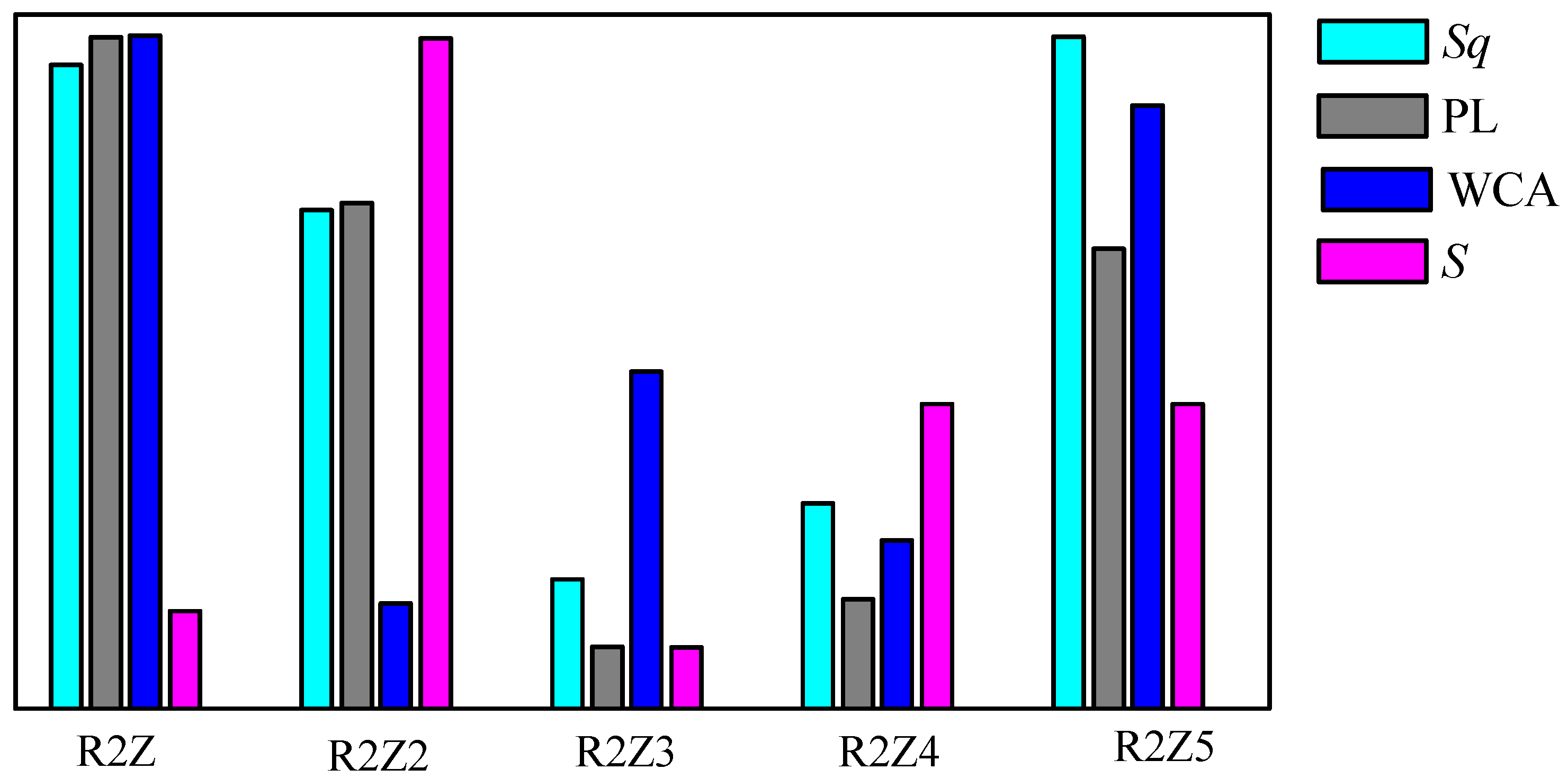
| Sample Code | Sq (nm) | S (Hz/ppm) | WCA (deg) |
|---|---|---|---|
| R2Z | 204 ± 5 | 0.026 ± 0.002 | 146 ± 0.9 |
| R2Z2 | 158 ± 4 | 0.12 ± 0.004 | 65 ± 0.1 |
| R2Z3 | 41 ± 2 | 0.02 ± 0.002 | 98 ± 0.6 |
| R2Z4 | 65 ± 3 | 0.06 ± 0.001 | 74 ± 1.2 |
| R2Z5 | 215 ± 5 | 0.06 ± 0.001 | 136 ± 0.7 |
Disclaimer/Publisher’s Note: The statements, opinions and data contained in all publications are solely those of the individual author(s) and contributor(s) and not of MDPI and/or the editor(s). MDPI and/or the editor(s) disclaim responsibility for any injury to people or property resulting from any ideas, methods, instructions or products referred to in the content. |
© 2024 by the authors. Licensee MDPI, Basel, Switzerland. This article is an open access article distributed under the terms and conditions of the Creative Commons Attribution (CC BY) license (https://creativecommons.org/licenses/by/4.0/).
Share and Cite
Marinov, G.; Alexieva, G.; Lazarova, K.; Gergova, R.; Ivanov, P.; Babeva, T. Optimization of Electrospray Deposition Conditions of ZnO Thin Films for Ammonia Sensing. Nanomaterials 2024, 14, 1008. https://doi.org/10.3390/nano14121008
Marinov G, Alexieva G, Lazarova K, Gergova R, Ivanov P, Babeva T. Optimization of Electrospray Deposition Conditions of ZnO Thin Films for Ammonia Sensing. Nanomaterials. 2024; 14(12):1008. https://doi.org/10.3390/nano14121008
Chicago/Turabian StyleMarinov, Georgi, Gergana Alexieva, Katerina Lazarova, Rositsa Gergova, Petar Ivanov, and Tsvetanka Babeva. 2024. "Optimization of Electrospray Deposition Conditions of ZnO Thin Films for Ammonia Sensing" Nanomaterials 14, no. 12: 1008. https://doi.org/10.3390/nano14121008
APA StyleMarinov, G., Alexieva, G., Lazarova, K., Gergova, R., Ivanov, P., & Babeva, T. (2024). Optimization of Electrospray Deposition Conditions of ZnO Thin Films for Ammonia Sensing. Nanomaterials, 14(12), 1008. https://doi.org/10.3390/nano14121008