Article

Exploration and Optimization of the Polymer-Modified NiOx Hole Transport Layer for Fabricating Inverted Perovskite Solar Cells

Institute of Lighting and Energy Photonics, College of Photonics, National Yang Ming Chiao Tung University, No. 301, Section 2, Gaofa 3rd Road, Guiren District, Tainan 711010, Taiwan
*
Author to whom correspondence should be addressed.
These authors contributed equally to this work.
Nanomaterials 2024, 14(12), 1054; https://doi.org/10.3390/nano14121054
Submission received: 31 May 2024 / Revised: 17 June 2024 / Accepted: 17 June 2024 / Published: 19 June 2024

Abstract

:
The recombination of charge carriers at the interface between carrier transport layers such as nickel oxide (NiOx) and the perovskite absorber has long been a challenge in perovskite solar cells (PSCs). To address this issue, we introduced a polymer additive poly(vinyl butyral) into NiOx and subjected it to high-temperature annealing to form a void-containing structure. The formation of voids is confirmed to increase light transmittance and surface area of NiOx, which is beneficial for light absorption and carrier separation within PSCs. Experimental results demonstrate that the incorporation of the polymer additive helped to enhance the hole conductivity and carrier extraction of NiOx with a higher Ni3+/Ni2+ ratio. This also optimized the energy levels of NiOx to match with the perovskite to raise the open-circuit voltage to 1.01 V. By incorporating an additional NiOx layer beneath the polymer-modified NiOx, the device efficiency was further increased as verified from the dark current measurement of devices.

Graphical Abstract

1. Introduction

Perovskite solar cells (PSCs) are widely recognized as one of the most promising photovoltaic technologies in the past decade, owing to their large light absorption coefficients in the visible spectrum, cost-effectiveness, long diffusion length, and facile fabrication [1,2,3,4]. Recently, the advent of organometallic halide PSCs has marked a significant advancement in achieving an impressive photovoltaic conversion efficiency (PCE) of 25.7–26.1% [5,6]. These achievements make PSCs exceptionally valuable for the upcoming generation of solar energy products.
Inverted PSCs, also known as p–i–n structures, are extensively investigated with the utilization of nickel oxide (NiOx) as the hole transport layer (HTL) [7,8]. Various techniques, including chemical bath deposition [9], the sol–gel method [10], plasma-assisted atomic layer deposition [11], spray pyrolysis [12], and nanoparticle dispersion [13], have been applied for the production of NiOx HTLs. Given the p-type and hole extraction nature of inorganic NiOx, scientists find its widespread use in inverted PSCs, which can be attributed to the existence of Ni vacancies in the lattices accompanying high transmittance in the visible range and environmental stability [3,14]. Although NiOx plays a pivotal role of hole extraction and transport in PSCs, there is still room for hole mobility improvement. As a result, the doping process and/or interfacial modification are employed to enhance hole mobility and extraction capabilities of NiOx, thereby reducing carrier recombination and achieving a superior performance of PSCs. To date, the interfacial modification of NiOx films has been implemented through combining NiOx with phthalocyanine or trimercapto-s-triazine trisodium salt [15,16]. On the other hand, transition metal doping such as Cu2+ [17,18], Ag+ [19], Co2+ [20,21], Mn2+ [22], and Zn2+ [23,24] have proven their effectiveness in enhancing the hole mobility of NiOx films as well as the photovoltaic performance of corresponding PSCs.
From the viewpoint of the mesoscopic junction in PSCs, there have been several studies concerning mesoporous structures of HTLs to improve charge extraction. Wang et al. reported the incorporation of a mesoscopic NiO layer to facilitate hole collection, enabling it to host the perovskite absorber and prevent the degradation of photovoltaic performance [25]. Liu, Shen, and their co-workers successfully utilized electrochemical deposition to form mesoporous NiOx films on FTO glass substrates, reducing carrier recombination and augmenting the photocurrent of devices [26]. Chen et al. deposited mesoporous CuGaO2 on the compact NiOx to form a double-layered HTL, as it effectively extracted holes from the perovskite due to the increased contact area at the HTL/perovskite interface [27]. Despite being a promising candidate for hole extraction and transport, surprisingly, there has been limited discussion about the formation of mesoporous NiOx HTLs involving organic polymers for fabricating PSCs.
Herein, we reported the preparation of void-containing NiOx by incorporating poly(vinyl butyral) (PVB) (denoted as p-NiOx) as the HTL. The mesoporous p-NiOx layer was obtained through high-temperature calcination at 500 °C, effectively enhancing both the transmittance of NiOx and hole transport within PSCs. To comprehensively investigate the impact of p-NiOx as the HTL in the photovoltaic devices, this study also explored the effects of PVB pretreatment on the interface between NiOx and the perovskite layer. Additionally, the original NiOx film (denoted as o-NiOx) and p-NiOx/o-NiOx films were prepared for comparative analysis. The experimental results reveal that the valence band (VB) of p-NiOx was shifted downwards compared to o-NiOx, which is demonstrated in Section 3.1, resulting in better alignment with the perovskite absorbing layer and a consequent increase in the open-circuit voltage (VOC) to 1.01 V. Furthermore, incorporating p-NiOx/o-NiOx thin films as the HTL demonstrated superior carrier transport capabilities to ameliorate charge extraction and reduced recombination in photovoltaic devices. While the device based on the o-NiOx HTL exhibited a moderate power conversion efficiency (PCE) of 14.84%, the utilization of the p-NiOx/o-NiOx structure resulted in a significantly improved PSC performance with the highest PCE of 16.46%.

2. Materials and Methods

Detailed information about the starting materials, preparation of perovskite layers, fabrication of PSCs, and characterization techniques is provided in the Supporting Information. The preparation of the o-NiOx and p-NiOx films is listed as follows. The o-NiOx film was prepared via the sol–gel process. Nickel acetate tetrahydrate (0.124 g), ethanolamine (30 μL), and ethanol (5 mL) were mixed in a sealed glass vial and heated at 70 °C until the solution color became translucent green. For the p-NiOx, 30 mg of PVB powder was added to the nickel acetate precursor solution. The two precursor films were deposited individually on the FTO substrates from their solutions via spin coating at 4500 rpm for 30 s under an ambient environment, followed by drying on a hotplate at 80 °C for 10 min. The substrates were then transferred into a tube furnace, heated from room temperature to 500 °C within 90 min in air, and sintered at the final temperature for 1 h to obtain the o-NiOx and p-NiOx films. Furthermore, a p-NiOx layer was deposited on top of the o-NiOx layer to form a p-NiOx/o-NiOx structure for comparison.

3. Results and Discussion

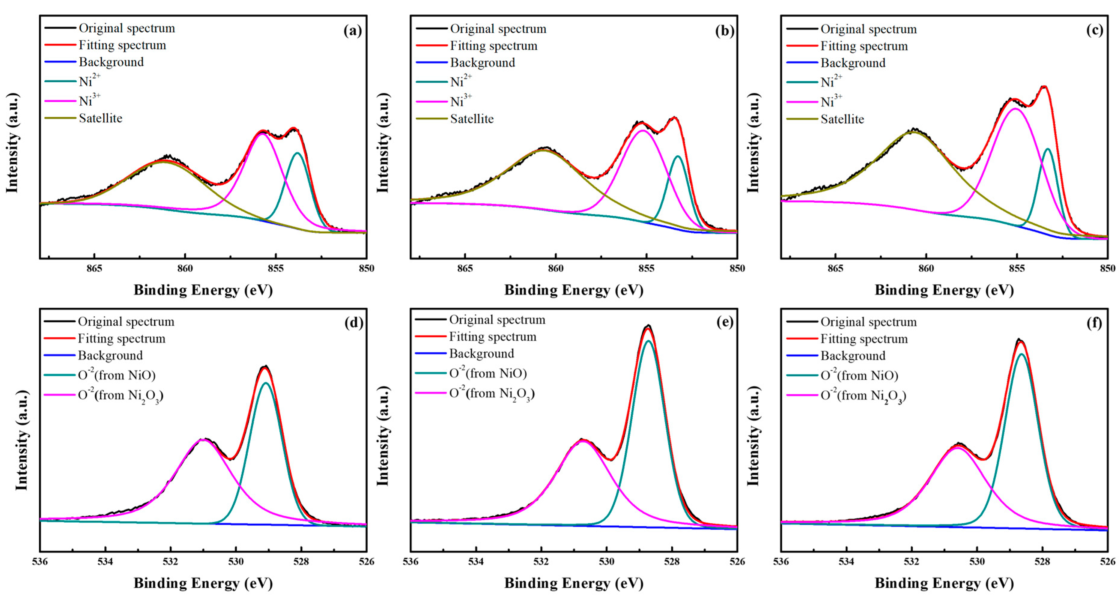
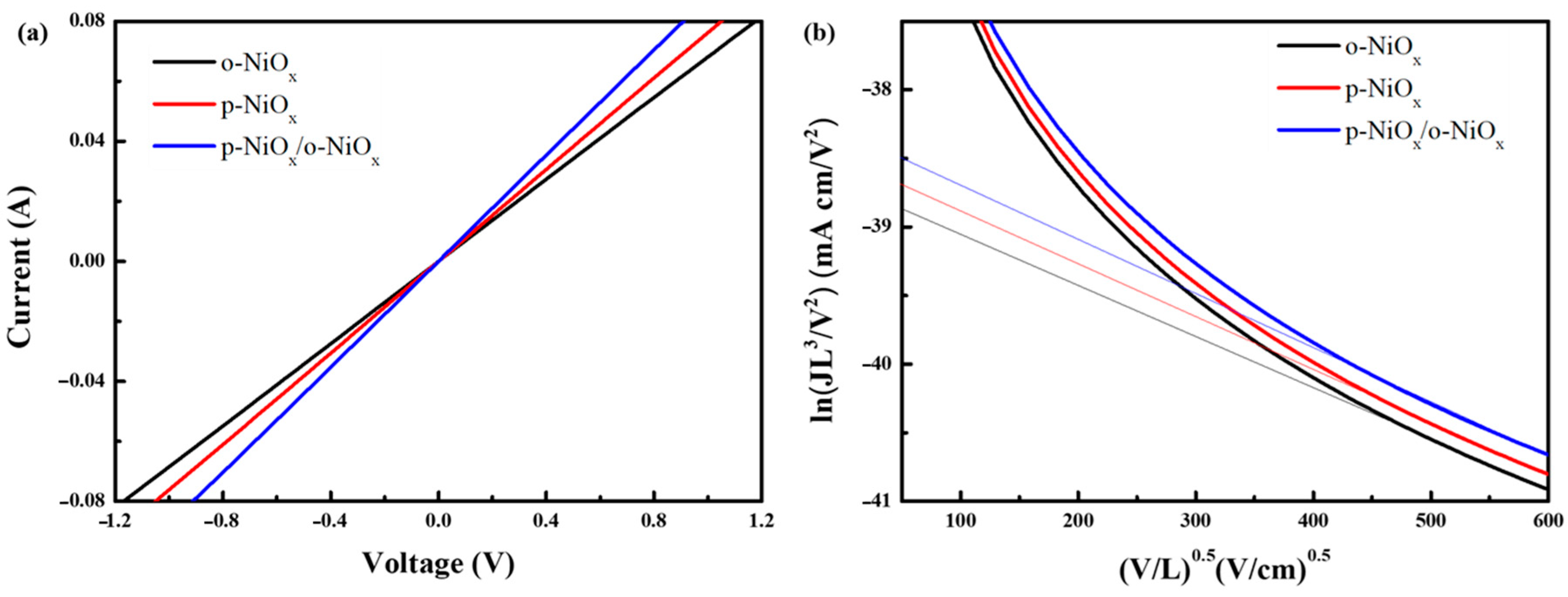
3.1. Characterization of the p-NiOx

The surface morphology and thickness of the o-NiOx and p-NiOx films on the FTO substrates were verified via scanning election microscopy (SEM) observation. The o-NiOx film with a thickness of 25 nm is very thin and hence the grains of low-lying FTO are clearly seen, as shown in Figure 1a,c. In Figure 1b,d, the p-NiOx showed uniformly distributed cracks on the surface with a thickness of 25 nm, which is close to that of the o-NiOx. The formation of voids is attributed to the thermal degradation of PVB during the calcination process of NiOx, which is supposed to increase the light transmittance and surface area of the resulting NiOx layer for the subsequent deposition of perovskite layers. Apart from the SEM observation, atomic force microscopy (AFM) experiments were also carried out to investigate the morphological properties and average roughness (Ra) of o-NiOx and p-NiOx films, as displayed in Figure 1e,f. The FTO grains are clearly observed for both samples; moreover, the o-NiOx has a Ra value of 14.9 nm, and the p-NiOx possesses a higher Ra value of 17.7 nm, possibly due to those cavities formed by the removal of PVB in the high-temperature calcination process [28]. Furthermore, X-ray diffraction (XRD) experiments were performed to examine the crystalline phases of the o-NiOx and p-NiOx and the corresponding XRD patterns are revealed in Figure S1 in the Supporting Information. Three diffraction peaks of NiOx are located at 2θ = 38.9, 42.5, and 64.5° in both XRD patterns, which corresponds to (111), (200), and (220) planes, respectively [29,30], confirming that the crystalline phase of the NiOx was not altered by PVB pretreatment.
The transmission and absorption spectra of the o-NiOx, p-NiOx and p-NiOx/o-NiOx films were measured to verify the effect of surface voids on their optical properties, which are depicted in Figure S2a. The transmittance of the o-NiOx was observed to be ca. 65% in the range of 350–700 nm. The p-NiOx film has the highest transmittance of 80–90% in the same visible range due to the existence of surface voids, as observed from SEM observation in Figure 1b. High transmittance is beneficial for incident photons to enter devices and to be absorbed by the perovskite absorbing layer. In addition, the p-NiOx/o-NiOx possesses a lower transmittance of 70–80% in the same range. This is reasonable since an additional NiOx layer was established below the p-NiOx layer. The absorption spectra of the o-NiOx, p-NiOx and p-NiOx/o-NiOx films are also displayed in Figure S2a, which look similar for the three NiOx films. The Tauc plots of different NiOx films are demonstrated in Figure S2b, indicating an optical bandgap of 3.8 eV for the o- NiOx layer and 3.73 eV for the p-NiOx and p-NiOx/o-NiOx films, which is close to the previous reports [29,31,32,33].
It is well known that the elemental state of Ni3+ (Ni2O3 species) can provide the nonstoichiometric NiOx with hole transport ability [34,35]. Therefore, the X-ray photoelectron spectroscopy (XPS) measurements were performed to investigate the effect of PVB pretreatment on the Ni3+/Ni2+ ratio as well as hole transport ability. The Ni 2p3/2 XPS spectra of the o-NiOx, p-NiOx and p-NiOx/o-NiOx films are displayed in Figure 2a−c. According to the previous literature [14,24,36], the multicomponent bands can be well fitted with three different states, including NiO (Ni 2p3/2 at 853.8 eV), Ni2O3 (Ni 2p3/2 at 855.3 eV), and a satellite peak of Ni3+ (at 856.1 eV). The Ni3+/Ni2+ ratios for the o-NiOx, p-NiOx and p-NiOx/o-NiOx films were calculated to be 2.17, 2.78 and 3.45, respectively, showing an apparent increasing Ni3+ proportion in the Ni 2p spectra after PVB pretreatment. Thus, the p-NiOx has a better hole-transporting capability than the pristine one [34,37]. Until now, the reason for the increased Ni3+/Ni2+ ratio up to 3.45 for the p-NiOx/o-NiOx remains unclear and more experiments should be implemented, such as electrical measurements of hole-only devices. The O 1s XPS spectra of the o-NiOx, p-NiOx and p-NiOx/o-NiOx films are presented in Figure 2d−f, revealing two prominent peaks at around 529 eV (O2– from NiO) and 531 eV (O2– from Ni2O3) [14,36]. In addition, the O2– peak from NiO shifted from 529.08 (o-NiOx) to 528.73 (p-NiOx) and 528.63 eV (p-NiOx/o-NiOx), implying possible interactions between PVB and NiOx via electronic transfer.
To further confirm the effect of PVB pretreatment on the single-carrier mobility and conductivity of NiOx, simple devices with three different configurations of FTO/o-NiOx/Ag, FTO/p-NiOx/Ag, and FTO/p-NiOx/o-NiOx/Ag devices were fabricated and their current−voltage (I−V) characteristics are illustrated in Figure 3a. The p-NiOx device possesses a larger slope than the o-NiOx, meaning that PVB pretreatment can improve the conductivity and charge transport ability of NiOx. In addition, the p-NiOx/o-NiOx device has the largest slope, indicative of the highest conductivity which is in accordance with XPS results. After calcination, the augmentation of the Ni3+ fraction facilitates carrier transport and brings about superior hole conductivity. Subsequently, the hole mobility (μh) of these films was approximated from the space charge limited current (SCLC) model defined as follows [38,39,40]:
J = ( 9 / 8 ) ε ε o μ h ( V 2 / L 3 )
where J is the current density, ε0 is the vacuum dielectric constant, and ε is the relative dielectric constant of NiOx [41]. V is the bias voltage, and L is the thickness of the NiOx film (∼25 nm). Figure 3b displays the electrical characteristics derived with the SCLC model of ln(JL3/V2) versus electric filed (V/L)0.5. The p-NiOx/o-NiOx structure has the highest μh of 1.62 × 10⁻² cm2/Vs, while the μh of the o-NiOx and p-NiOx are calculated to be 1.11 × 10⁻² and 1.22 × 10⁻² cm2/Vs, respectively. The augmented μh value of the NiOx HTL is expected to bring on the improvement in PCE and device performance of PSCs [22].
The energy levels and work functions (φw) of the o-NiOx, p-NiOx and p-NiOx/o-NiOx films were implemented via the ultraviolet photoelectron spectroscopy (UPS) analysis. The UPS spectra of different NiOx films in the high- and low-binding energy regions are shown in Figure 4a. The φw can be obtained through subtracting the high-binding energy cutoff (around 17 eV) from the photon energy of the He I source (21.22 eV) [42,43]. Therefore, the φw of the o-NiOx, p-NiOx and p-NiOx/o-NiOx films is determined to be 4.06, 4.08, and 3.99 eV, respectively. It is known that the work function represents the energy difference between vacuum energy levels and the Fermi level (EF) [44,45,46]. The energy difference between the valence band (VB) level and the φw is associated with the low-binding energy cutoff (around 1 eV) [22]. Ergo, the VB of the o-NiOx, p-NiOx and p-NiOx/o-NiOx films were calculated to be −5.2, −5.24 and −5.31 eV, respectively. The energy level diagram of the different NiOx and the perovskite layers is depicted in Figure 4b, which is comparable to the previous literature [11,22,24,25]. The alignment of energy levels is crucial for optimizing hole extraction and transport efficiency in PSCs. Reducing the energy barrier between the perovskite layer and HTL would decrease the energy loss during charge transport [27]. The p-NiOx/o-NiOx exhibits an obviously downshifted VB level which aligns well with the perovskite layer (VB = −5.4 eV), meaning that better hole extraction can be achieved using PVB pretreatment and consequently a higher VOC is anticipated [18].

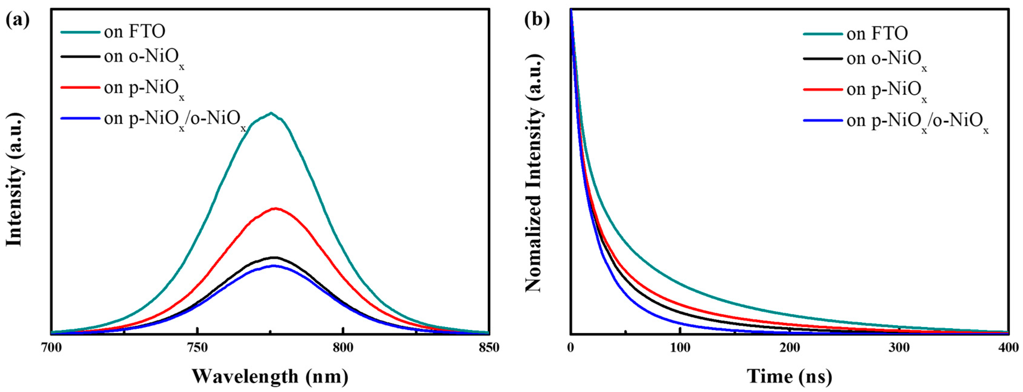
3.2. Characterization of Perovskite Layers on NiOx

To analyze the crystallinity and topography of perovskite layers on different NiOx HTLs, the XRD and SEM experiments were conducted. The corresponding XRD patterns and top-view SEM images of perovskite layers are provided in Figures S3 and S4. Several intense diffraction peaks at 2θ = 13.95°, 19.86°, 24.58°, 28.33°, 31.82°, 34.91°, 40.51°, and 43.12° were found, corresponding to the (001), (011), (111), (002), (012), (112), (022), and (003) planes of the perovskite, respectively, which are consistent with the previous literature [47,48,49]. Furthermore, the perovskite grains on the o-NiOx, p-NiOx and p-NiOx/o-NiOx films appear similar in Figure S4. It is known that the NiOx films remained unaltered after PVB pretreatment (see XRD patterns Figure S1) and PVB was removed during the calcination process, and likewise, there would be no significant change in the morphological structure of the perovskite. To conclude, the XRD patterns and top-view SEM images of perovskites on the three NiOx HTLs look similar, implying that the p-NiOx and p-NiOx/o-NiOx structures have little or no effect on the crystalline property and morphology of the perovskite.
Figure 5a displays the steady-state photoluminescence (PL) spectra of the perovskites deposited on the FTO, o-NiOx, p-NiOx, and p-NiOx/o-NiOx films. It can be seen that the perovskite deposited on the FTO substrate has the highest PL emission, while the one on the o-NiOx has a lower PL intensity. According to the previous literature, the decrease in PL intensity means an enhanced charge extraction and transport from the perovskite layer to the HTL [18,22]. It seems odd that the perovskite on the p-NiOx possesses the second strongest PL intensity. It is conjectured that the existence of voids led to direct contact between the perovskite and FTO substrate to reduce the carrier extraction ability of NiOx. At the same time, the perovskite on the p-NiOx/o-NiOx structure has the lowest PL emission, bringing about the improved photovoltaic performance of PSCs. To further verify the PL results of perovskite films on different NiOx films, the time-resolved PL (TR-PL) decay experiments were carried out and the corresponding PL decay curves are shown in Figure 5b. It is seen that the perovskite coated on the p-NiOx/o-NiOx structure possessed the fastest PL decay curve compared with other NiOx films, implying that the hole–electron separation was accomplished more effectively [17]. The TR-PL decay curves were fitted using a biexponential model; the fast decay constant τ1 and slow decay constant τ2 represent the surface recombination and charge recombination in the perovskite bulk, respectively [50,51]. Then, the average carrier lifetime (τavg) was estimated from the equation τ a v g   = ( A i τ i 2 ) ( A i τ i ) , where Ai and τi were deduced from the data of the fitted curve [52,53,54]. All the acquired decay constants τ1, τ2 and τayg are summarized in Table S1 in the Supplementary Information. The τavg was calculated to be 84.13, 45.25, 53.72 and 31.14 ns for the perovskite layers on the FTO, o-NiOx, p-NiOx, and p-NiOx/o-NiOx films, respectively. Since the carrier lifetime is inversely proportional to charge extraction, the p-NiOx/o-NiOx structure has the best charge extraction capability among all NiOx films, suggesting the highest device performance of PSCs [11,19].

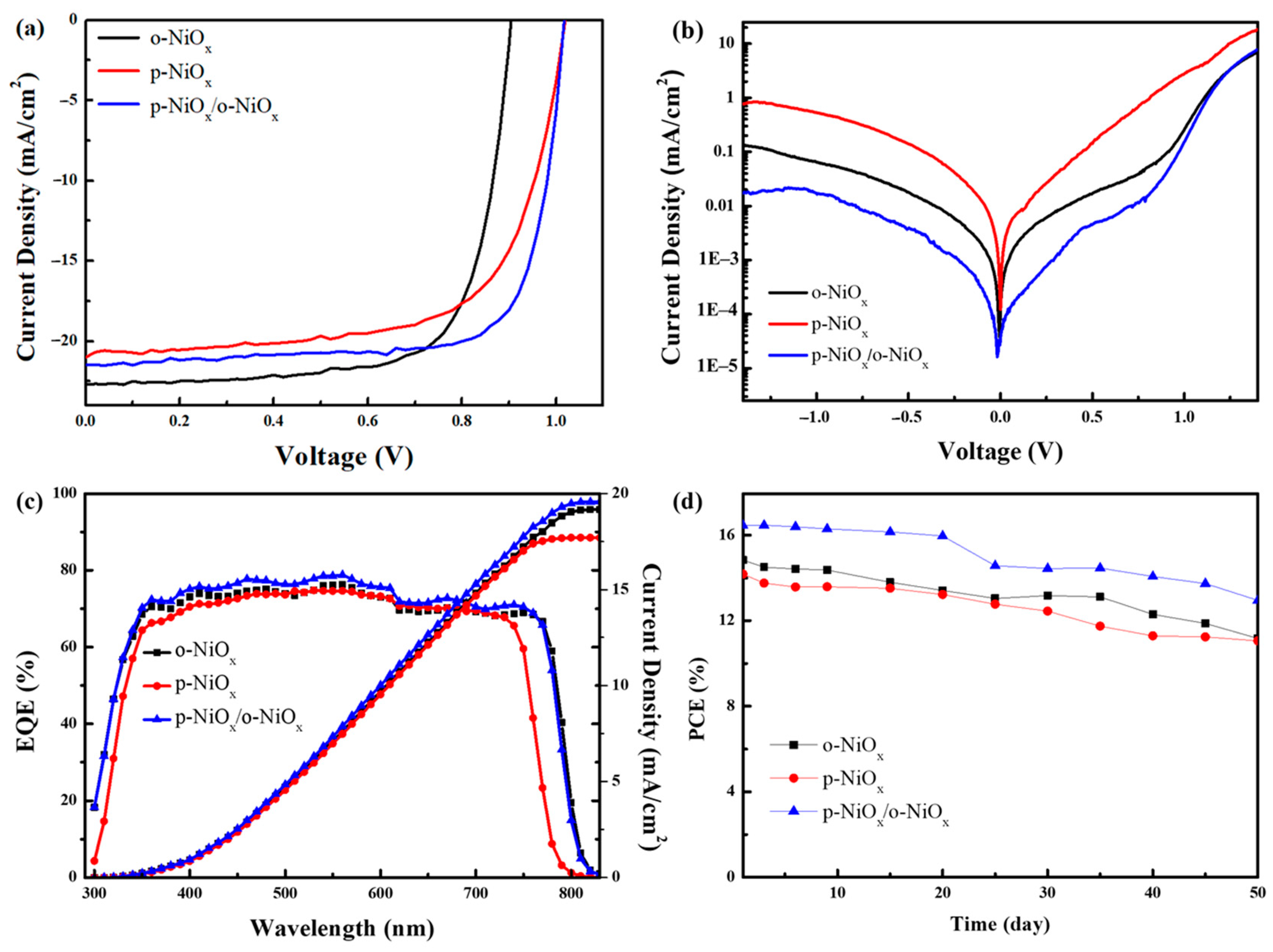
3.3. Device Evaluation

The planar p–i–n PSCs with the architecture of FTO/o-NiOx, p-NiOx or p-NiOx/o-NiOx/perovskite/PC61BM+TBABF4/PEI/Ag were fabricated and evaluated in this study. The cross-sectional SEM image of the whole device is presented in Figure S5 to estimate the thickness of each layer. A thickness of 25, 550, 40, 20 and 100 nm is obtained for the p-NiOx, perovskite, TBABF4-doped PCBM, and the PEI and Ag electrode, respectively. The thickness of the p-NiOx/o-NiOx is approximately double that of the p-NiOx layer. Figure 6a presents the current density−voltage (J−V) curves of PSCs based on the o-NiOx, p-NiOx or p-NiOx/o-NiOx structures as the HTL under AM 1.5G illumination, and Table 1 summarizes the photovoltaic parameters of all devices including JSC, VOC, FF, and PCE. The control device using the o-NiOx HTL displayed a moderate PCE of 14.8%, a JSC of 22.7 mA/cm2, a VOC of 0.9 V, and an FF value of 72%. The best photovoltaic performance was achieved from the device using the p-NiOx/o-NiOx HTL, revealing a PCE of 16.5% which is significantly higher than other devices in this study. The JSC, VOC and FF of the device based on the p-NiOx/o-NiOx HTL were measured to be 21.5 mA/cm2, 1.01 V, and 75%, respectively. As for the device using the p-NiOx HTL, the JSC, VOC, FF, and PCE are 21.0 mA/cm2, 1.01 V, 66%, and 14.2%, respectively. Figure S6 depicts the statistical distribution for JSC, VOC, FF and PCE from 20 individual devices. To realize the hysteresis effect, the J–V curves of devices were measured in the reverse and forward scans and corresponding results are displayed in Figure S7 and Table S2. The hysteresis index (HI) is calculated using the equation HI = (PCEreverse − PCEforward)/PCEreverse, and the device based on p-NiOx/o-NiOx has the smallest HI value of 0.09, indicating that the hysteresis phenomenon is reduced through using the p-NiOx/o-NiOx bilayered structure as the HTL. Our PSCs maintained good reproducibility and the device based on the p-NiOx/o-NiOx HTL showed relatively higher photovoltaic parameters. The improvement in the device performance can be interpreted from several aspects. As previously discussed in the XPS section, the p-NiOx/o-NiOx has the largest Ni3+/Ni2+ ratio and hole transport ability, leading to the enhanced efficiency of PSCs. In the discussion of UPS experiments, the p-NiOx/o-NiOx exhibits the smallest φw as well as matched energy level with the perovskite absorbing layer, thereby facilitating hole extraction from the perovskite to the HTL. Furthermore, the electrical measurements of the p-NiOx/o-NiOx device indicate an elevated μh which is beneficial for the carrier transport and PCE of devices. Considering the above aspects, the device using the p-NiOx/o-NiOx HTL exhibited the best performance as anticipated. To validate the leakage current of devices, dark current measurements were performed and the corresponding results are displayed in Figure 6b. As mentioned in the previous parts, we assumed that using the p-NiOx HTL would encounter an issue of void formation, which could be verified using dark current measurements. The reverse currents from low to high belong to the devices using p-NiOx/NiOx, o-NiOx, and p-NiOx as the HTL. It is evident that the PSC using p-NiOx has a larger leakage current than that using o-NiOx as the HTL. While the PSC based on p-NiOx/NiOx possesses the lowest dark current, it conveys benefits for reducing recombination loss and enhancing carrier transport [48,55]. According to the previous literature [56,57], the values of the series resistance (Rs) and shunt resistance (Rsh) of PSCs can be determined from the voltage dependence of the differential resistance (Rdiff) using the equation Rdiff = Δ V/Δ J, as displayed in Figure S8. The Rs is determined using the extrapolation of the saturated part of the RdiffV curve toward the interception with the resistance axis. The Rsh is equal to the differential resistance at a bias of 0 V. It is concluded that the device based on the p-NiOx/o-NiOx HTL has the largest Rsh value of 8.35 kΩcm2 among the three PSCs, indicative of the best device performance. Figure 6c shows the integrated current densities and external quantum efficiency (EQE) spectra of devices using o-NiOx, p-NiOx, and p-NiOx/NiOx as the HTL. The results attest that the EQE maximum of the device using p-NiOx/NiOx achieved about 79% at 550 nm, being the highest spectral line across the visible range. Furthermore, the integrated current densities of 19.17, 17.7, 19.58 mA/cm2 were obtained from the devices based on the o-NiOx, p-NiOx, and p-NiOx/NiOx HTLs, respectively. To explore long-term stability, the unencapsulated PSCs were stored in the nitrogen glovebox and their J–V characteristics under AM 1.5G exposure were measured in ambient air. Figure 6d records the PCE evolution of the PSCs based on the o-NiOx, p-NiOx, and p-NiOx/NiOx HTLs. All devices maintained about 70% of their initial efficiency over a period of 50 days. It is noted that the PCE of the fresh PSC based on the p-NiOx/NiOx HTL was 16.4% and it dropped to 13% after 50 days of storage, remaining the best performance among the three devices.

4. Conclusions

We have successfully prepared the p-NiOx film with surface voids to increase light transmittance and the interfacial area, facilitating the subsequent deposition of perovskite layers. The p-NiOx HTL exhibited elevated carrier mobility and a downward VB shift, significantly enhancing hole transport behavior and reducing the energy barrier between p-NiOx and the perovskite absorber. On the other hand, the usage of the p-NiOx thin film may encounter direct contact between the perovskite and FTO, as deduced from the result of dark current measurements. Among the three NiOx HTLs, the device based on the p-NiOx/o-NiOx HTL possessed the lowest leakage current and the best charge extraction capability. Additionally, the highest VOC of 1.01 V, a PCE of 16.5%, and a good device lifetime of up to 50 days were received, presenting the best performance among the three PSCs.

Supplementary Materials

The following supporting information can be downloaded at: https://www.mdpi.com/article/10.3390/nano14121054/s1, Figure S1: XRD patterns of the o-NiOx and p-NiOx films on the FTO substrates, Figure S2: Absorption and transmission spectra, Tauc plots of the o-NiOx, p-NiOx and p-NiOx/o-NiOx films deposited on the FTO substrates, Figure S3: XRD patterns of perovskite layers on the o-NiOx, p-NiOx and p-NiOx/o-NiOx films, Figure S4: Top-view SEM images of perovskite layers on the o-NiOx, p-NiOx, and p-NiOx/o-NiOx films, Figure S5: Cross-sectional SEM micrograph of the whole device with p-NiOx, Figure S6: Performance variation is represented as a standard box plot in PCE, JSC, FF, and VOC from 20 devices based on the o-NiOx, p-NiOx and p-NiOx/o-NiOx films, Figure S7: J−V characteristics of PSCs based on the o-NiOx, p-NiOx and p-NiOx/o-NiOx HTLs in the reverse and forward scans under AM 1.5G exposure, Figure S8: Differential resistance Rdiff versus voltage of devices in the dark. Table S1: Lifetime parameters of TR-PL curves of the perovskite on the FTO substrate, o-NiOx, p-NiOx, and p-NiOx/o-NiOx structure, Table S2: Device performance of inverted PSCs based on the o-NiOx, p-NiOx and p-NiOx/o-NiOx films as the HTL in the reverse and forward scans.

Author Contributions

Conceptualization, Y.-W.W.; methodology, C.-Y.W.; investigation, Y.-W.W.; formal analysis, Y.-W.W. and C.-Y.W.; resources, S.-H.Y.; supervision, S.-H.Y.; validation, S.-H.Y.; writing—original draft, Y.-W.W. and C.-Y.W.; writing—review and editing, S.-H.Y. All authors have read and agreed to the published version of the manuscript.

Funding

The authors thank the National Science and Technology Council of Taiwan, Republic of China under Contract No. NSTC 110-2221-E-A49-082-MY3 for financially supporting this work.

Data Availability Statement

The original contributions presented in the study are included in the article/Supplementary Material, further inquiries can be directed to the corresponding author.

Conflicts of Interest

There are no conflicts to declare.

References

  1. Lin, Q.; Armin, A.; Nagiri, R.C.R.; Burn, P.L.; Meredith, P. Electro-optics of perovskite solar cells. Nat. Photonics 2015, 9, 106–112. [Google Scholar] [CrossRef]
  2. Liu, B.; Wang, Y.; Wu, Y.; Dong, B.; Song, H. Novel broad spectral response perovskite solar cells: A review of the current status and advanced strategies for breaking the theoretical limit efficiency. J. Mater. Sci. Technol. 2023, 140, 33–57. [Google Scholar] [CrossRef]
  3. Park, H.; Chaurasiya, R.; Jeong, B.H.; Sakthivel, P.; Park, H.J. Nickel Oxide for Perovskite Photovoltaic Cells. Adv. Photonics Res. 2021, 2, 2000178. [Google Scholar] [CrossRef]
  4. Jiang, Q.; Zhang, X.; You, J. SnO2: A Wonderful Electron Transport Layer for Perovskite Solar Cells. Small 2018, 14, 1801154. [Google Scholar] [CrossRef]
  5. National Renewable Energy Laboratory (NREL). Efficiency Chart. 2024. Available online: https://www.nrel.gov/pv/cell-efficiency.html (accessed on 2 May 2024).
  6. Hou, Y.; Aydin, E.; De Bastiani, M.; Xiao, C.; Isikgor, F.H.; Xue, D.-J.; Chen, B.; Chen, H.; Bahrami, B.; Chowdhury, A.H.; et al. Efficient tandem solar cells with solution-processed perovskite on textured crystalline silicon. Science 2020, 367, 1135–1140. [Google Scholar] [CrossRef]
  7. Pu, X.; Zhao, J.; Li, Y.; Zhang, Y.; Loi, H.-L.; Wang, T.; Chen, H.; He, X.; Yang, J.; Ma, X.; et al. Stable NiOx-based inverted perovskite solar cells achieved by passivation of multifunctional star polymer. Nano Energy 2023, 112, 108506. [Google Scholar] [CrossRef]
  8. Mali, S.S.; Kim, H.; Kim, H.H.; Shim, S.E.; Hong, C.K. Nanoporous p-type NiOx electrode for p-i-n inverted perovskite solar cell toward air stability. Mater. Today 2018, 21, 483–500. [Google Scholar] [CrossRef]
  9. Li, L.; Shen, W.; Yang, C.; Dou, Y.; Zhu, X.; Dong, Y.; Zhao, J.; Xiao, J.; Huang, F.; Cheng, Y.-B.; et al. In-situ monitored chemical bath deposition of planar NiOx layer for inverted perovskite solar cell with enhanced efficiency. J. Mater. Sci. Technol. 2023, 133, 145–153. [Google Scholar] [CrossRef]
  10. Gidey, A.T.; Kuo, D.-W.; Fenta, A.D.; Chen, C.-T.; Chen, C.-T. First Conventional Solution Sol–Gel-Prepared Nanoporous Materials of Nickel Oxide for Efficiency Enhancing and Stability Extending MAPbI3 Inverted Perovskite Solar Cells. ACS Appl. Energy Mater. 2021, 4, 6486–6499. [Google Scholar] [CrossRef]
  11. Koushik, D.; Jošt, M.; Dučinskas, A.; Burgess, C.; Zardetto, V.; Weijtens, C.; Verheijen, M.A.; Kessels, W.M.M.; Albrecht, S.; Creatore, M. Plasma-assisted atomic layer deposition of nickel oxide as hole transport layer for hybrid perovskite solar cells. J. Mater. Chem. C 2019, 7, 12532–12543. [Google Scholar] [CrossRef]
  12. Ukoba, K.O.; Eloka-Eboka, A.C.; Inambao, F.L. Review of nanostructured NiO thin film deposition using the spray pyrolysis technique. Renew. Sustain. Energy Rev. 2018, 82, 2900–2915. [Google Scholar] [CrossRef]
  13. Cai, C.; Zhou, K.; Guo, H.; Pei, Y.; Hu, Z.; Zhang, J.; Zhu, Y. Enhanced hole extraction by NiO nanoparticles in carbon-based perovskite solar cells. Electrochim. Acta 2019, 312, 100–108. [Google Scholar] [CrossRef]
  14. Yin, X.; Guo, Y.; Xie, H.; Que, W.; Kong, L.B. Nickel Oxide as Efficient Hole Transport Materials for Perovskite Solar Cells. Sol. RRL 2019, 3, 1900001. [Google Scholar] [CrossRef]
  15. Zhao, X.; Zhang, W.; Feng, X.; Guo, X.; Lu, C.; Li, X.; Fang, J. Photoconductive NiOx hole transport layer for efficient perovskite solar cells. Chem. Eng. J. 2022, 435, 135140. [Google Scholar] [CrossRef]
  16. Yang, J.; Wang, T.; Li, Y.; Pu, X.; Chen, H.; Li, Y.; Yang, B.; Zhang, Y.; Zhao, J.; Cao, Q.; et al. Overcome Low Intrinsic Conductivity of NiOx Through Triazinyl Modification for Highly Efficient and Stable Inverted Perovskite Solar Cells. Sol. RRL 2022, 6, 2200422. [Google Scholar] [CrossRef]
  17. Huang, A.; Lei, L.; Chen, Y.; Yu, Y.; Zhou, Y.; Liu, Y.; Yang, S.; Bao, S.; Li, R.; Jin, P. Minimizing the energy loss of perovskite solar cells with Cu+ doped NiOx processed at room temperature. Sol. Energy Mater. Sol. Cells 2018, 182, 128–135. [Google Scholar] [CrossRef]
  18. Kim, J.H.; Liang, P.-W.; Williams, S.T.; Cho, N.; Chueh, C.-C.; Glaz, M.S.; Ginger, D.S.; Jen, A.K.-Y. High-Performance and Environmentally Stable Planar Heterojunction Perovskite Solar Cells Based on a Solution-Processed Copper-Doped Nickel Oxide Hole-Transporting Layer. Adv. Mater. 2015, 27, 695–701. [Google Scholar] [CrossRef]
  19. Wei, Y.; Yao, K.; Wang, X.; Jiang, Y.; Liu, X.; Zhou, N.; Li, F. Improving the efficiency and environmental stability of inverted planar perovskite solar cells via silver-doped nickel oxide hole-transporting layer. Appl. Surf. Sci. 2018, 427, 782–790. [Google Scholar] [CrossRef]
  20. Xie, Y.; Lu, K.; Duan, J.; Jiang, Y.; Hu, L.; Liu, T.; Zhou, Y.; Hu, B. Enhancing Photovoltaic Performance of Inverted Planar Perovskite Solar Cells by Cobalt-Doped Nickel Oxide Hole Transport Layer. ACS Appl. Mater. Interfaces 2018, 10, 14153–14159. [Google Scholar] [CrossRef]
  21. Purushothaman, K.K.; Muralidharan, G. Electrochromic properties of nickel oxide and mixed Co/Ni oxide films prepared via sol–gel route. J. Non-Cryst. Solids 2012, 358, 354–359. [Google Scholar] [CrossRef]
  22. Wu, Y.-W.; Chang, C.-Y.; Chiu, F.-B.; Yang, S.-H. Efficient and stable perovskite solar cells using manganese-doped nickel oxide as the hole transport layer. RSC Adv. 2022, 12, 22984–22995. [Google Scholar] [CrossRef]
  23. Lee, J.H.; Noh, Y.W.; Jin, I.S.; Jung, J.W. Efficient planar heterojunction perovskite solar cells employing a solution-processed Zn-doped NiOX hole transport layer. Electrochim. Acta 2018, 284, 253–259. [Google Scholar] [CrossRef]
  24. Wan, X.; Jiang, Y.; Qiu, Z.; Zhang, H.; Zhu, X.; Sikandar, I.; Liu, X.; Chen, X.; Cao, B. Zinc as a New Dopant for NiOx-Based Planar Perovskite Solar Cells with Stable Efficiency near 20%. ACS Appl. Energy Mater. 2018, 1, 3947–3954. [Google Scholar] [CrossRef]
  25. Wang, K.-C.; Jeng, J.-Y.; Shen, P.-S.; Chang, Y.-C.; Diau, E.W.-G.; Tsai, C.-H.; Chao, T.-Y.; Hsu, H.-C.; Lin, P.-Y.; Chen, P.; et al. p-type Mesoscopic Nickel Oxide/Organometallic Perovskite Heterojunction Solar Cells. Sci. Rep. 2014, 4, 4756. [Google Scholar] [CrossRef]
  26. Wang, T.; Ding, D.; Wang, X.; Zeng, R.; Liu, H.; Shen, W. High-Performance Inverted Perovskite Solar Cells with Mesoporous NiOx Hole Transport Layer by Electrochemical Deposition. ACS Omega 2018, 3, 18434–18443. [Google Scholar] [CrossRef]
  27. Chen, Y.; Yang, Z.; Wang, S.; Zheng, X.; Wu, Y.; Yuan, N.; Zhang, W.-H.; Liu, S.F. Design of an Inorganic Mesoporous Hole-Transporting Layer for Highly Efficient and Stable Inverted Perovskite Solar Cells. Adv. Mater. 2018, 30, 1805660. [Google Scholar] [CrossRef]
  28. El-Din, N.M.S.; Sabaa, M.W. Thermal degradation of poly(viny1 butyral) laminated safety glass. Polym. Degrad. Stabil. 1995, 41, 283–288. [Google Scholar] [CrossRef]
  29. Kim, K.H.; Takahashi, C.; Abe, Y.; Kawamura, M. Effects of Cu doping on nickel oxide thin film prepared by sol–gel solution process. Optik 2014, 125, 2899–2901. [Google Scholar] [CrossRef]
  30. Yadav, M.S.; Tripathi, S.K. Synthesis and characterization of nanocomposite NiO/activated charcoal electrodes for supercapacitor application. Ionics 2017, 23, 2919–2930. [Google Scholar] [CrossRef]
  31. Meybodi, S.M.; Hosseini, S.A.; Rezaee, M.; Sadrnezhaad, S.K.; Mohammadyani, D. Synthesis of wide band gap nanocrystalline NiO powder via a sonochemical method. Ultrason. Sonochem. 2012, 19, 841–845. [Google Scholar] [CrossRef]
  32. Sasi, B.; Gopchandran, K.G. Preparation and characterization of nanostructured NiO thin films by reactive-pulsed laser ablation technique. Sol. Energy Mater. Sol. Cells 2007, 91, 1505–1509. [Google Scholar] [CrossRef]
  33. Chen, S.C.; Kuo, T.Y.; Lin, Y.C.; Lin, H.C. Preparation and properties of p-type transparent conductive Cu-doped NiO films. Thin Solid Film. 2011, 519, 4944–4947. [Google Scholar] [CrossRef]
  34. Chen, W.; Liu, F.-Z.; Feng, X.-Y.; Djurišić, A.B.; Chan, W.K.; He, Z.-B. Cesium Doped NiOx as an Efficient Hole Extraction Layer for Inverted Planar Perovskite Solar Cells. Adv. Energy Mater. 2017, 7, 1700722. [Google Scholar] [CrossRef]
  35. Guo, Y.; Ma, J.; Wang, H.; Ye, F.; Xiong, L.; Lei, H.; Tan, Z. Overcoming Ni3+-Induced Non-Radiative Recombination at Perovskite-Nickel Oxide Interfaces to Boost Voltages in Perovskite Solar Cells. Adv. Mater. Interfaces 2021, 8, 2100920. [Google Scholar] [CrossRef]
  36. Dubey, P.; Kaurav, N.; Devan, R.S.; Okram, G.S.; Kuo, Y.K. The effect of stoichiometry on the structural thermal and electronic properties of thermally decomposed nickel oxide. RSC Adv. 2018, 8, 5882–5890. [Google Scholar] [CrossRef]
  37. Xie, L.; Cao, Z.; Wang, J.; Wang, A.; Wang, S.; Cui, Y.; Xiang, Y.; Niu, X.; Hao, F.; Ding, L. Improving energy level alignment by adenine for efficient and stable perovskite solar cells. Nano Energy 2020, 74, 104846. [Google Scholar] [CrossRef]
  38. Ma, J.; Zheng, M.; Chen, C.; Zhu, Z.; Zheng, X.; Chen, Z.; Guo, Y.; Liu, C.; Yan, Y.; Fang, G. Efficient and Stable Nonfullerene-Graded Heterojunction Inverted Perovskite Solar Cells with Inorganic Ga2O3 Tunneling Protective Nanolayer. Adv. Funct. Mater. 2018, 28, 1804128. [Google Scholar] [CrossRef]
  39. Xiong, S.; Yuan, M.; Yang, J.; Song, J.; Guo, X.; Li, X.; Li, B.; Liu, X.; Duan, C.; Liu, F.; et al. Engineering of the Back Contact between PCBM and Metal Electrode for Planar Perovskite Solar Cells with Enhanced Efficiency and Stability. Adv. Opt. Mater. 2019, 7, 1900542. [Google Scholar] [CrossRef]
  40. Hung, C.-M.; Lin, J.-T.; Yang, Y.-H.; Liu, Y.-C.; Gu, M.-W.; Chou, T.-C.; Wang, S.-F.; Chen, Z.-Q.; Wu, C.-C.; Chen, L.-C.; et al. Modulation of Perovskite Grain Boundaries by Electron Donor–Acceptor Zwitterions R,R-Diphenylamino-phenyl-pyridinium-(CH2)n-sulfonates: All-Round Improvement on the Solar Cell Performance. JACS Au 2022, 2, 1189–1199. [Google Scholar] [CrossRef]
  41. Ye, L.-H.; Luo, N.; Peng, L.-M. Dielectric constant of NiO and LDA+U. Phys. Rev. B 2013, 87, 075115. [Google Scholar]
  42. Schlaf, R.; Parkinson, B.A.; Lee, P.A.; Nebesny, K.W.; Jabbour, G.; Kippelen, B.; Peyghambarian, N.; Armstrong, N.R. Photoemission spectroscopy of LiF coated Al and Pt electrodes. J. Appl. Phys. 1998, 84, 6729–6736. [Google Scholar] [CrossRef]
  43. Schroeder, P.G.; France, C.B.; Parkinson, B.A.; Schlaf, R. Orbital alignment at p-sexiphenyl and coronene/layered materials interfaces measured with photoemission spectroscopy. J. Appl. Phys. 2002, 91, 9095–9107. [Google Scholar] [CrossRef]
  44. Shao, G. Work Function and Electron Affinity of Semiconductors: Doping Effect and Complication due to Fermi Level Pinning. Energy Environ. Mater. 2021, 4, 273–276. [Google Scholar] [CrossRef]
  45. Kashiwaya, S.; Morasch, J.; Streibel, V.; Toupance, T.; Jaegermann, W.; Klein, A. The Work Function of TiO2. Surfaces 2018, 1, 73–89. [Google Scholar] [CrossRef]
  46. Klein, A.; Albe, K.; Bein, N.; Clemens, O.; Creutz, K.A.; Erhart, P.; Frericks, M.; Ghorbani, E.; Hofmann, J.P.; Huang, B.; et al. The Fermi energy as common parameter to describe charge compensation mechanisms: A path to Fermi level engineering of oxide electroceramic. J. Electroceram 2023, 51, 147–177. [Google Scholar] [CrossRef]
  47. Zhumekenov, A.A.; Saidaminov, M.I.; Haque, M.A.; Alarousu, E.; Sarmah, S.P.; Murali, B.; Dursun, I.; Miao, X.-H.; Abdelhady, A.L.; Wu, T.; et al. Formamidinium Lead Halide Perovskite Crystals with Unprecedented Long Carrier Dynamics and Diffusion Length. ACS Energy Lett. 2016, 1, 32–37. [Google Scholar] [CrossRef]
  48. She, Z.-X.; Yang, S.-H. Interfacial modification between NiOx and perovskite layers with hexafluorophosphate salts for enhancing device efficiency and stability of perovskite solar cells. RSC Appl. Interfaces 2024, 1, 443–454. [Google Scholar] [CrossRef]
  49. Zheng, G.; Zhu, C.; Ma, J.; Zhang, X.; Tang, G.; Li, R.; Chen, Y.; Li, L.; Hu, J.; Hong, J.; et al. Manipulation of facet orientation in hybrid perovskite polycrystalline films by cation cascade. Nat. Commun. 2018, 9, 2793. [Google Scholar] [CrossRef]
  50. Dong, P.; Yuan, S.; Zhu, D.; Du, Y.; Mu, C.; Ai, X.-C. Electron transport layer assisted by nickel chloride hexahydrate for open-circuit voltage improvement in MAPbI3 perovskite solar cells. RSC Adv. 2022, 12, 13820–13825. [Google Scholar] [CrossRef]
  51. Chen, P.; Bai, Y.; Wang, S.; Lyu, M.; Yun, J.-H.; Wang, L. In Situ Growth of 2D Perovskite Capping Layer for Stable and Efficient Perovskite Solar Cells. Adv. Funct. Mater. 2018, 28, 1706923. [Google Scholar] [CrossRef]
  52. Zheng, J.; Hu, L.; Yun, J.S.; Zhang, M.; Lau, C.F.J.; Bing, J.; Deng, X.; Ma, Q.; Cho, Y.; Fu, W.; et al. Solution Processed, Silver Doped NiOx as Hole Transporting Layer for High-Efficiency Inverted Perovskite Solar Cells. ACS Appl. Energy Mater. 2018, 1, 561–570. [Google Scholar] [CrossRef]
  53. Abate, S.Y.; Yang, Z.; Jha, S.; Emodogo, J.; Ma, G.; Ouyang, Z.; Muhammad, S.; Pradhan, N.; Gu, X.; Patton, D.; et al. Promoting Large-Area Slot-Die-Coated Perovskite Solar Cell Performance and Reproducibility by Acid-Based Sulfono-γ-AApeptide. ACS Appl. Mater. Interfaces 2023, 15, 25495–25505. [Google Scholar] [CrossRef]
  54. Lee, D.G.; Kim, M.-C.; Kim, B.J.; Kim, D.H.; Lee, S.M.; Choi, M.; Lee, S.; Jung, H.S. Effect of TiO2 particle size and layer thickness on mesoscopic perovskite solar cells. Appl. Surf. Sci. 2019, 477, 131–136. [Google Scholar] [CrossRef]
  55. Ke, W.; Stoumpos, C.C.; Spanopoulos, I.; Chen, M.; Wasielewski, M.R.; Kanatzidis, M.G. Diammonium Cations in the FASnI3 Perovskite Structure Lead to Lower Dark Currents and More Efficient Solar Cells. ACS Energy Lett. 2018, 3, 1470–1476. [Google Scholar] [CrossRef]
  56. Vollbrecht, J.; Brus, V.V.; Ko, S.-J.; Lee, J.; Karki, A.; Cao, D.X.; Cho, K.; Bazan, G.C.; Nguyen, T.-Q. Quantifying the Nongeminate Recombination Dynamics in Nonfullerene Bulk Heterojunction Organic Solar Cells. Adv. Energy Mater. 2019, 9, 1901438. [Google Scholar] [CrossRef]
  57. Brus, V.V.; Proctor, C.M.; Ran, N.A.; Nguyen, T.-Q. Capacitance Spectroscopy for Quantifying Recombination Losses in Nonfullerene Small-Molecule Bulk Heterojunction Solar Cells. Adv. Energy Mater. 2016, 6, 1502250. [Google Scholar] [CrossRef]
Figure 1. Top-view and cross-sectional SEM images of the (a,c) o-NiOx and (b,d) p-NiOx thin films deposited on the FTO substrates; AFM topographic images of the (e) o-NiOx and (f) p-NiOx thin films.
Nanomaterials 14 01054 g001
Figure 2. XPS spectra of (ac) Ni 2p3/2 and (df) O 1s elements in the o-NiOx, p-NiOx and p-NiOx/o-NiOx.
Nanomaterials 14 01054 g002
Figure 3. (a) Linear sweep voltammetry curves of devices based on the o-NiOx, p-NiOx and p-NiOx/o-NiOx films; (b) hole mobility of the o-NiOx, p-NiOx and p-NiOx/o-NiOx films versus electric field (V/L)0.5.
Nanomaterials 14 01054 g003
Figure 4. (a) UPS spectra of the o-NiOx, p-NiOx, and p-NiOx/o-NiOx films; (b) energy level diagram of the whole device (unit: eV).
Nanomaterials 14 01054 g004
Figure 5. (a) PL emission spectra and (b) TR-PL decay curves of the perovskites on the FTO, o-NiOx, p-NiOx and p-NiOx/o-NiOx films.
Nanomaterials 14 01054 g005
Figure 6. (a) J−V characteristics under AM 1.5G exposure, (b) dark J−V curves, (c) EQE spectra and integrated current density, and (d) PCE evolution of devices based on the o-NiOx, p-NiOx and p-NiOx/o-NiOx HTLs.
Nanomaterials 14 01054 g006
Table 1. Device performance of inverted PSCs based on the o-NiOx, p-NiOx and p-NiOx/o-NiOx films as the HTL.
HTLJSC (mA/cm2)JSC from EQE (mA/cm2)VOC (V)FF (%)Best PCE (%)Avg. PCE a (%)
o-NiOx22.719.20.907214.814.1
p-NiOx21.017.71.016614.213.5
p-NiOx/o-NiOx21.519.61.017516.515.6
a The average PCE was obtained from 20 devices.
Disclaimer/Publisher’s Note: The statements, opinions and data contained in all publications are solely those of the individual author(s) and contributor(s) and not of MDPI and/or the editor(s). MDPI and/or the editor(s) disclaim responsibility for any injury to people or property resulting from any ideas, methods, instructions or products referred to in the content.

