
WS2 with Controllable Layer Number Grown Directly on W Film
Abstract
:1. Introduction
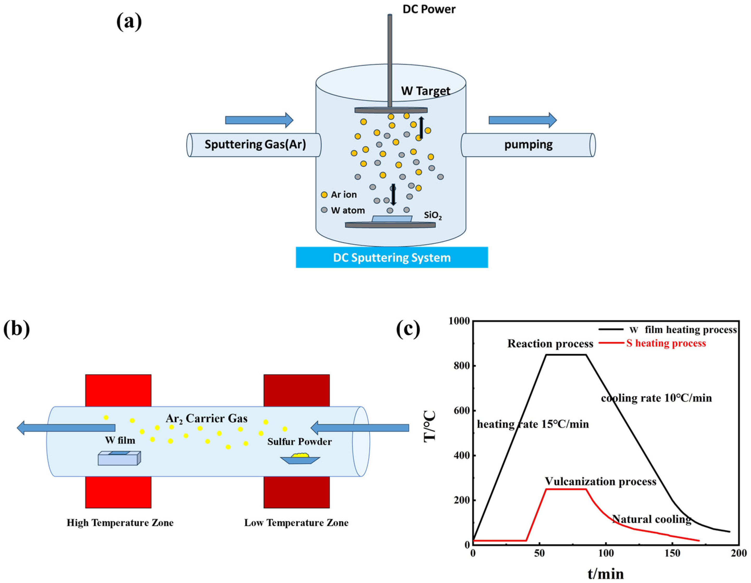
2. Experiment
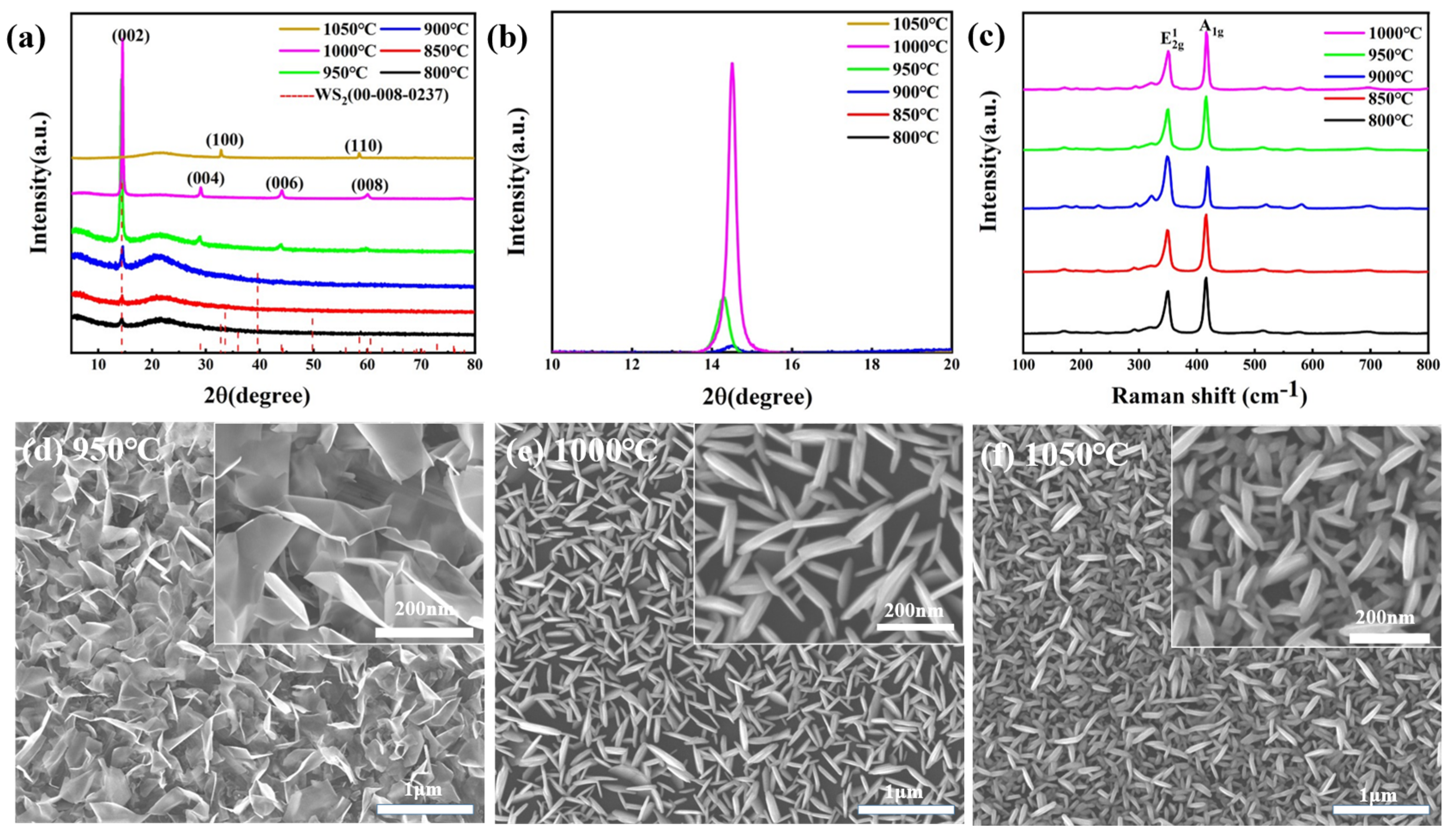
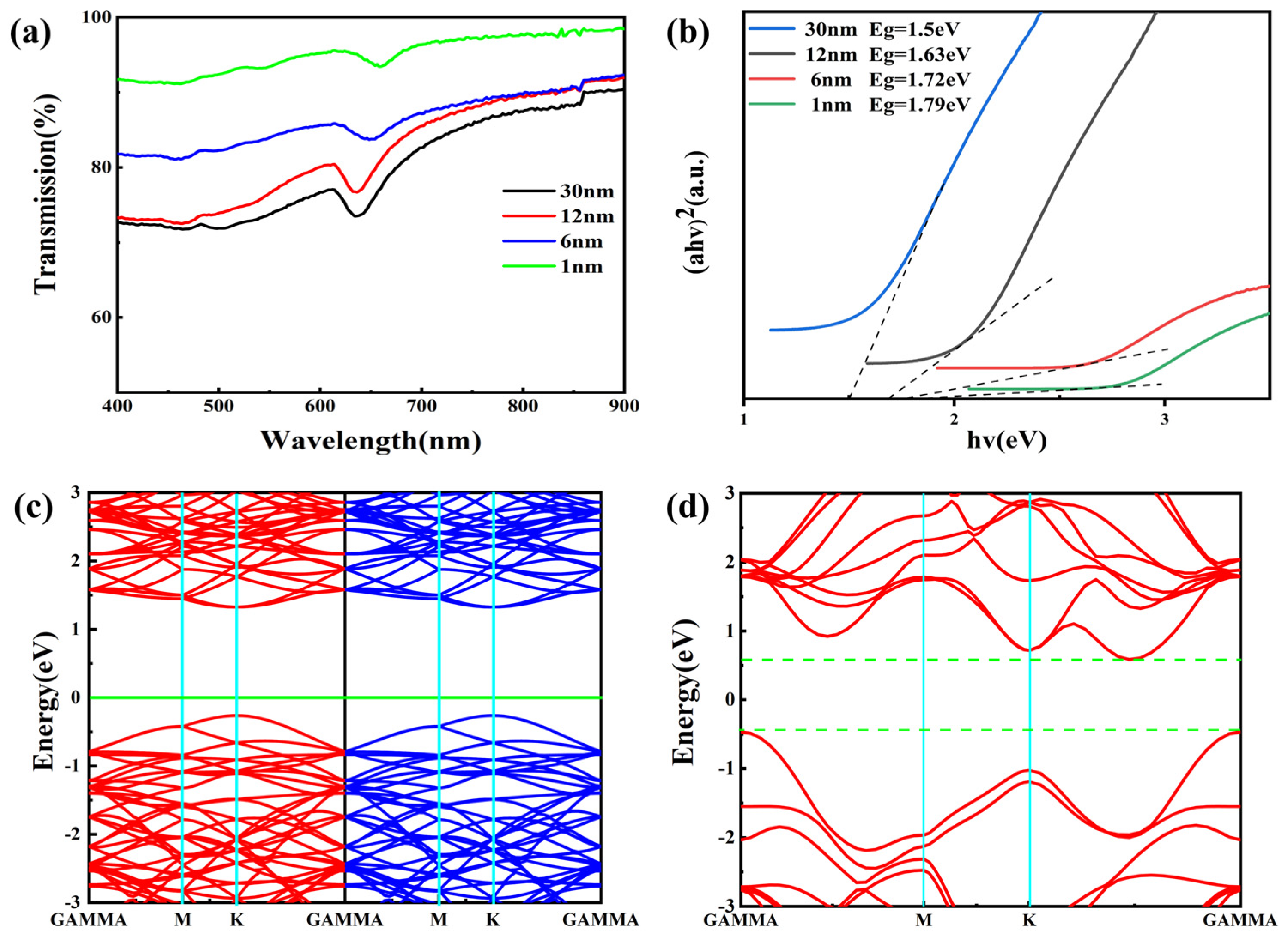
3. Results and Discussion
4. Conclusions
Author Contributions
Funding
Data Availability Statement
Conflicts of Interest
References
- Kumar, V.; Mishra, R.K.; Choi, G.J.; Ryu, J.W.; Kumar, P.; Gwag, J.S. Optical and dielectric response of two-dimensional WX2 (X = Cl, O, S, Se, Te) monolayers: A comprehensive study based on density functional theory. Luminescence 2023, 38, 1368–1373. [Google Scholar] [CrossRef] [PubMed]
- Zhang, B.; Luo, C.; Deng, Y.Q.; Huang, Z.J.; Zhou, G.M.; Lv, W.; He, Y.B.; Wan, Y.; Kang, F.Y.; Yang, Q.H. Optimized Catalytic WS2-WO3 Heterostructure Design for Accelerated Polysulfide Conversion in Lithium-Sulfur Batteries. Adv. Energy Mater. 2020, 10, 8. [Google Scholar] [CrossRef]
- Cho, E.; Nguyen, A.T.; Lim, S.; Cho, J.; Song, J.; Kwon, S.; Kim, D.W. Thickness-dependent optical characteristics of WS2 flakes prepared by Au- and Ag-assisted exfoliation. J. Phys. D Appl. Phys. 2023, 56, 8. [Google Scholar] [CrossRef]
- Faraduan, I.; Handayani, I.P.; Diandra, D.A.; Delima, H.; Fathona, I.W. Electronic properties of hybrid WS2/MoS2 multilayer on flexible PET. Mater. Res. Express 2021, 8, 6. [Google Scholar] [CrossRef]
- Li, N.; Feng, L.P.; Su, J.; Zeng, W.; Liu, Z.T. Optical and electrical properties of Al:WS2 films prepared by atomic layer deposition and vulcanization. RSC Adv. 2016, 6, 64879–64884. [Google Scholar] [CrossRef]
- Lei, W.; Xiao, J.L.; Liu, H.P.; Jia, Q.L.; Zhang, H.J. Tungsten disulfide: Synthesis and applications in electrochemical energy storage and conversion. Tungsten 2020, 2, 217–239. [Google Scholar] [CrossRef]
- Jiang, T.; Yin, K.; Wang, C.; You, J.; Ouyang, H.; Miao, R.L.; Zhang, C.X.; Wei, K.; Li, H.; Chen, H.T.; et al. Ultrafast fiber lasers mode-locked by two-dimensional materials: Review and prospect. Photonics Res. 2020, 8, 78–90. [Google Scholar] [CrossRef]
- Day, R.W.; Bediako, D.K.; Rezaee, M.; Parent, L.R.; Skorupskii, G.; Arguilla, M.Q.; Hendon, C.H.; Stassen, I.; Gianneschi, N.C.; Kim, P.; et al. Single Crystals of Electrically Conductive Two-Dimensional Metal-Organic Frameworks: Structural and Electrical Transport Properties. ACS Central Sci. 2019, 5, 1959–1964. [Google Scholar] [CrossRef]
- Burch, K.S.; Mandrus, D.; Park, J.G. Magnetism in two-dimensional van der Waals materials. Nature 2018, 563, 47–52. [Google Scholar] [CrossRef]
- Gong, C.; Li, L.; Li, Z.L.; Ji, H.W.; Stern, A.; Xia, Y.; Cao, T.; Bao, W.; Wang, C.Z.; Wang, Y.A.; et al. Discovery of intrinsic ferromagnetism in two-dimensional van der Waals crystals. Nature 2017, 546, 265–269. [Google Scholar] [CrossRef]
- Fu, Q.; Bao, X.H. Surface chemistry and catalysis confined under two-dimensional materials. Chem. Soc. Rev. 2017, 46, 1842–1874. [Google Scholar] [CrossRef]
- Finge, T.; Riederer, F.; Mueller, M.R.; Grap, T.; Kallis, K.; Knoch, J. Investigations on Field-Effect Transistors Based on Two-Dimensional Materials. Ann. Phys. 2017, 529, 10. [Google Scholar] [CrossRef]
- Li, M.J.; Xu, Y.M.; Zhao, B.; Wu, C.X.; Zhou, Q.X.; Wang, Z.W.; Li, T.W.; Ju, W.W. Exploration of electrical contact type in two-dimensional WS2/Nb2CX2 (X = H, F, Cl) heterostructures. Appl. Surf. Sci. 2022, 602, 10. [Google Scholar] [CrossRef]
- Akinwande, D.; Huyghebaert, C.; Wang, C.H.; Serna, M.I.; Goossens, S.; Li, L.J.; Wong, H.S.P.; Koppens, F.H.L. Graphene and two-dimensional materials for silicon technology. Nature 2019, 573, 507–518. [Google Scholar] [CrossRef] [PubMed]
- Shu, H.B. Structural stability, tunable electronic and optical properties of two-dimensional WS2 and GaN heterostructure: First-principles calculations. Mater. Sci. Eng. B Adv. Funct. Solid State Mater. 2020, 261, 8. [Google Scholar] [CrossRef]
- Ansari, N.; Mohebbi, E.; Nazari, E. The role of the defect in photonic crystals based on WS2 or WSe2 monolayers: A vision on how to achieve high quality factor and wavelength adjustability in defect modes. Opt. Quantum Electron. 2023, 55, 16. [Google Scholar] [CrossRef]
- Li, H.L.; Cui, Y.T.; Li, W.J.; Ye, L.J.; Mu, L. Strain-tunable band alignment of blue phosphorus-WX2 (X = S/Se/Te) vertical heterostructures: From first-principles study. Appl. Phys. A Mater. Sci. Process. 2020, 126, 10. [Google Scholar] [CrossRef]
- Zhang, Z.W.; Chen, P.; Duan, X.D.; Zang, K.T.; Luo, J.; Duan, X.F. Robust epitaxial growth of two-dimensional heterostructures, multiheterostructures, and superlattices. Science 2017, 357, 788–792. [Google Scholar] [CrossRef] [PubMed]
- Moradpur-Tari, E.; Sarraf-Mamoory, R.; Yourdkhani, A. Structural, electronic, and electrochemical studies of WS2 phases using density functional theory and machine learning. Physica B 2023, 650, 12. [Google Scholar] [CrossRef]
- Su, L.Q.; Bradley, L.; Yu, Y.L.; Yu, Y.F.; Cao, L.Y.; Zhao, Y.P.; Zhang, Y. Surface-enhanced Raman scattering of monolayer transition metal dichalcogenides on Ag nanorod arrays. Opt. Lett. 2019, 44, 5493–5496. [Google Scholar] [CrossRef]
- Sethulekshmi, A.S.; Jayan, J.S.; Saritha, A.; Joseph, K. Insights into the reinforcibility and multifarious role of WS2 in polymer matrix. J. Alloys Compd. 2021, 876, 15. [Google Scholar] [CrossRef]
- Jian, J.Y.; Nan, Y.X.; Dong, P.F.; Feng, H.; Zuo, K.N.A.; Chang, H.L. Dependence of the photoelectric performance of the CVD-grown 2D WS2 on the oxygen-doping concentration. J. Alloys Compd. 2022, 895, 10. [Google Scholar] [CrossRef]
- Kim, S.E.; Mujid, F.; Rai, A.; Eriksson, F.; Suh, J.; Poddar, P.; Ray, A.; Park, C.; Fransson, E.; Zhong, Y.; et al. Extremely anisotropic van der Waals thermal conductors. Nature 2021, 597, 660–665. [Google Scholar] [CrossRef] [PubMed]
- Sharma, D.K.; Kumar, S.; Auluck, S. Electronic structure, defect properties, and hydrogen storage capacity of 2H-WS2: A first-principles study. Int. J. Hydrogen Energy 2018, 43, 23126–23134. [Google Scholar] [CrossRef]
- Tian, J.Y.; Lu, K.; Liu, X.J. Hybrid heterostructure of transition metal dichalcogenides as potential photocatalyst for hydrogen evolution. Appl. Surf. Sci. 2022, 599, 11. [Google Scholar] [CrossRef]
- Wang, F.; Niu, S.W.; Liang, X.Q.; Wang, G.M.; Chen, M.H. Phosphorus incorporation activates the basal plane of tungsten disulfide for efficient hydrogen evolution catalysis. Nano Res. 2022, 15, 2855–2861. [Google Scholar] [CrossRef]
- Zhou, J.; Cao, J.M.; Shi, J.N.; Zhang, Y.F.; Chen, J.Y.; Wang, W.Q.; Liu, X.W. A WS2 Case Theoretical Study: Hydrogen Storage Performance Improved by Phase Altering. Nanoscale Res. Lett. 2020, 15, 8. [Google Scholar] [CrossRef]
- Liu, W.L.; Benson, J.; Dawson, C.; Strudwick, A.; Raju, A.P.A.; Han, Y.S.; Li, M.X.; Papakonstantinou, P. The effects of exfoliation, organic solvents and anodic activation on the catalytic hydrogen evolution reaction of tungsten disulfide. Nanoscale 2017, 9, 13515–13526. [Google Scholar] [CrossRef] [PubMed]
- Kumar, Y.A.; Mani, G.; Pallavolu, M.R.; Sambasivam, S.; Nallapureddy, R.R.; Selvaraj, M.; Alfakeer, M.; Bahajjaj, A.A.A.; Ouladsmane, M.; Rao, S.S.; et al. Facile synthesis of highly efficient construction of tungsten disulfide/iron cobaltite nanocomposite grown on nickel foam as a battery-type energy material for electrochemical supercapacitors with superior performance. J. Colloid Interface Sci. 2022, 609, 434–446. [Google Scholar] [CrossRef]
- Han, A.L.; Zhou, X.F.; Wang, X.J.; Liu, S.; Xiong, Q.H.; Zhang, Q.H.; Gu, L.; Zhuang, Z.C.; Zhang, W.J.; Li, F.X.; et al. One-step synthesis of single-site vanadium substitution in 1T-WS2 monolayers for enhanced hydrogen evolution catalysis. Nat. Commun. 2021, 12, 10. [Google Scholar] [CrossRef]
- Wu, E.P.; Wu, D.; Jia, C.; Wang, Y.G.; Yuan, H.Y.; Zeng, L.H.; Xu, T.T.; Shi, Z.F.; Tian, Y.T.; Li, X.J. In Situ Fabrication of 2D WS2/Si Type-II Heterojunction for Self-Powered Broadband Photodetector with Response up to Mid-Infrared. ACS Photonics 2019, 6, 565–572. [Google Scholar] [CrossRef]
- Zhong, Y.Y.; Shao, Y.L.; Ma, F.K.; Wu, Y.Z.; Huang, B.B.; Hao, X.P. Band-gap-matched CdSe QD/WS2 nanosheet composite: Size-controlled photocatalyst for high-efficiency water splitting. Nano Energy 2017, 31, 84–89. [Google Scholar] [CrossRef]
- Thiehmed, Z.A.; Altahtamouni, T.M. Morphology Control of WS2 Nanoflakes Using Chemical Vapor Deposition for Improving the Photocatalytic Activity of the WS2/TiO2 Heterostructure. J. Phys. Chem. C 2023, 127, 9. [Google Scholar] [CrossRef]
- Wree, J.L.; Glauber, J.P.; Ohl, D.; Niesen, A.; Kostka, A.; Rogalla, D.; Schuhmann, W.; Devi, A. Sensing and electrocatalytic activity of tungsten disulphide thin films fabricated via metal-organic chemical vapour deposition. J. Mater. Chem. C 2021, 9, 10254–10265. [Google Scholar] [CrossRef]
- Zhu, M.; Huang, K.; Zhou, K.-G. Lifting the mist of flatland: The recent progress in the characterizations of two-dimensional materials. Prog. Cryst. Growth Charact. Mater. 2017, 63, 72–93. [Google Scholar] [CrossRef]
- Qu, S.; Zhang, J.; Gao, L.; Chen, H.; Ding, Y. Effect of Deposition Pressure and Temperature on Tungsten Thin-Film Heater for Phase-Change Switch Applications. Micromachines 2024, 15, 576. [Google Scholar] [CrossRef] [PubMed]
- Luo, M.; Xie, T.; Li, X.; Zheng, L.; Du, T.; Zhang, Z.; Yang, J. Compatible camouflage for dual-band guided-laser radar and infrared via a metamaterial perfect absorber. Optics Express 2024, 32, 11221–11240. [Google Scholar] [CrossRef]
- Huang, S.; Long, C.; Hu, Z.; Xu, Y.; Zhang, B.; Zhi, C. Thermal Performance of Heat Sink Filled with Double-Porosity Porous Aluminum Skeleton/Paraffin Phase Change Material. Micromachines 2024, 15, 806. [Google Scholar] [CrossRef]
- Qu, S.; Gao, L.; Wang, J.; Chen, H.; Zhang, J. A Review on Material Selection Benchmarking in GeTe-Based RF Phase-Change Switches for Each Layer. Micromachines 2024, 15, 380. [Google Scholar] [CrossRef] [PubMed]
- Ye, Z.; Yang, J.; Sun, J.; Hu, B.; Zhou, S. An optical scheme of on-chip matrixing by phase-change based tunable weighting of photonic tensor unit. J. Phys. D Appl. Phys. 2023, 56, 455104. [Google Scholar] [CrossRef]
- Adomaviciute-Grabusove, S.; Popov, A.; Ramanavicius, S.; Sablinskas, V.; Shevchuk, K.; Gogotsi, O.; Baginskiy, I.; Gogotsi, Y.; Ramanavicius, A. Monitoring Ti3C2Tx MXene Degradation Pathways Using Raman Spectroscopy. ACS Nano 2024, 18, 13184–13195. [Google Scholar] [CrossRef] [PubMed]
- Li, L.J.; Zhang, G.J.; Younis, M.; Luo, T.Y.; Yang, L.; Jin, W.; Wu, H.; Xiao, B.C.; Zhang, W.F.; Chang, H.X. 2D Tellurium Films Based Self-Drive Near Infrared Photodetector. ChemPhysChem 2024, 25, e202400383. [Google Scholar] [CrossRef] [PubMed]
- Dong, L.Q.; Wang, Y.Y.; Sun, J.C.; Pan, C.F.; Zhang, Q.H.; Gu, L.; Wan, B.S.; Song, C.; Pan, F.; Wang, C.; et al. Facile access to shape-controlled growth of WS2 monolayer via environment-friendly method. 2D Mater. 2019, 6, 9. [Google Scholar]
- Ding, Q.; Song, B.; Xu, P.; Jin, S. Efficient Electrocatalytic and Photoelectrochemical Hydrogen Generation Using MoS2 and Related Compounds. Chem 2016, 1, 699–726. [Google Scholar] [CrossRef]
- Yu, W.L.; Gao, Y.X.; Chen, Z.; Zhao, Y.; Wu, Z.X.; Wang, L. Strategies on improving the electrocatalytic hydrogen evolution performances of metal phosphides. Chin. J. Catal. 2021, 42, 1876–1902. [Google Scholar] [CrossRef]
- Yue, L.; Xu, D.; Wei, Z.Y.; Zhao, T.T.; Lin, T.; Tenne, R.; Zak, A.; Li, Q.N.; Liu, B.B. Size and Shape’s Effects on the High-Pressure Behavior of WS2 Nanomaterials. Materials 2022, 15, 2838. [Google Scholar] [CrossRef]
- Zhao, H.; Wu, H.; Wu, J.H.; Li, J.L.; Wang, Y.J.; Zhang, Y.; Liu, H. Preparation of MoS2/WS2 nanosheets by liquid phase exfoliation with assistance of epigallocatechin gallate and study as an additive for high-performance lithium-sulfur batteries. J. Colloid Interface Sci. 2019, 552, 554–562. [Google Scholar] [CrossRef] [PubMed]
- Zhang, Y.; Yao, Y.Y.; Sendeku, M.G.; Yin, L.; Zhan, X.Y.; Wang, F.; Wang, Z.X.; He, J. Recent Progress in CVD Growth of 2D Transition Metal Dichalcogenides and Related Heterostructures. Adv. Mater. 2019, 31, 30. [Google Scholar] [CrossRef] [PubMed]
- Govindasamy, M.; Wang, S.F.; Alothman, A.A.; Alshgari, R.A.; Ganesh, P.S. Synergetic effect of the ultrasonic-assisted hydrothermal process on the photocatalytic performance of MoS2 and WS2 nanoparticles. J. Mater. Sci. Mater. Electron. 2022, 33, 8858–8867. [Google Scholar] [CrossRef]
- Villamayor, M.M.S.; Lindblad, A.; Johansson, F.O.L.; Tran, T.; Pham, N.H.; Primetzhofer, D.; Sorgenfrei, N.L.A.N.; Giangrisotomi, E.; Föhlisch, A.; Lourenço, P.; et al. Growth of two-dimensional WS2 thin films by reactive sputtering. Vacuum 2021, 188, 110205. [Google Scholar] [CrossRef]
- Hunag, J.; Xie, S.; Cheng, X.; Li, Y.; Hu, C.; Qi, Z. An optical spectrum study of interlayer interaction in WS2/WSe2 heterostructure. J. Univ. Sci. Technol. China 2019, 49, 452–457. [Google Scholar]
- Ma, L.; Jia, J.; Chen, W.; Li, X.; Xu, Z. Hydrothermal synthesis and characterization of WS2 nanoribbons. J. Zhejiang Univ. (Eng. Sci.) 2006, 40, 832–835. [Google Scholar]
- Tian, K.; Baskaran, K.; Tiwari, A. Growth of two-dimensional WS2 thin films by pulsed laser deposition technique. Thin Solid Films 2018, 668, 69–73. [Google Scholar] [CrossRef]
- Yan, H.T.; Li, J.H.; Liu, D.M.; Jing, X.N.; Wang, D.Q.; Meng, L.J. Controlled preparation of high quality WS2 nanostructures by a microwave-assisted solvothermal method. Crystengcomm 2018, 20, 2324–2330. [Google Scholar] [CrossRef]
- Bocharov, D.; Piskunov, S.; Zhukovskii, Y.F.; Evarestov, R.A. Ab Initio Calculations on the Electronic Structure and Photocatalytic Properties of Two-Dimensional WS2 (0001) Nanolayers of Varying Thickness. Phys. Status Solidi (RRL) Rapid Res. Lett. 2018, 13, 1800253. [Google Scholar] [CrossRef]


| Precursor Thickness (nm) | Frequency Difference (cm−1) |
|---|---|
| 1 | 67.542 |
| 6 | 67.057 |
| 12 | 66.582 |
| 30 | 65.794 |
Disclaimer/Publisher’s Note: The statements, opinions and data contained in all publications are solely those of the individual author(s) and contributor(s) and not of MDPI and/or the editor(s). MDPI and/or the editor(s) disclaim responsibility for any injury to people or property resulting from any ideas, methods, instructions or products referred to in the content. |
© 2024 by the authors. Licensee MDPI, Basel, Switzerland. This article is an open access article distributed under the terms and conditions of the Creative Commons Attribution (CC BY) license (https://creativecommons.org/licenses/by/4.0/).
Share and Cite
Zhang, Y.; Feng, S.; Guo, J.; Tao, R.; Liu, Z.; He, X.; Wang, G.; Wang, Y. WS2 with Controllable Layer Number Grown Directly on W Film. Nanomaterials 2024, 14, 1356. https://doi.org/10.3390/nano14161356
Zhang Y, Feng S, Guo J, Tao R, Liu Z, He X, Wang G, Wang Y. WS2 with Controllable Layer Number Grown Directly on W Film. Nanomaterials. 2024; 14(16):1356. https://doi.org/10.3390/nano14161356
Chicago/Turabian StyleZhang, Yuxin, Shiyi Feng, Jin Guo, Rong Tao, Zhixuan Liu, Xiangyi He, Guoxia Wang, and Yue Wang. 2024. "WS2 with Controllable Layer Number Grown Directly on W Film" Nanomaterials 14, no. 16: 1356. https://doi.org/10.3390/nano14161356