
Two-Dimensional Semiconductors for State-of-the-Art Complementary Field-Effect Transistors and Integrated Circuits

Abstract
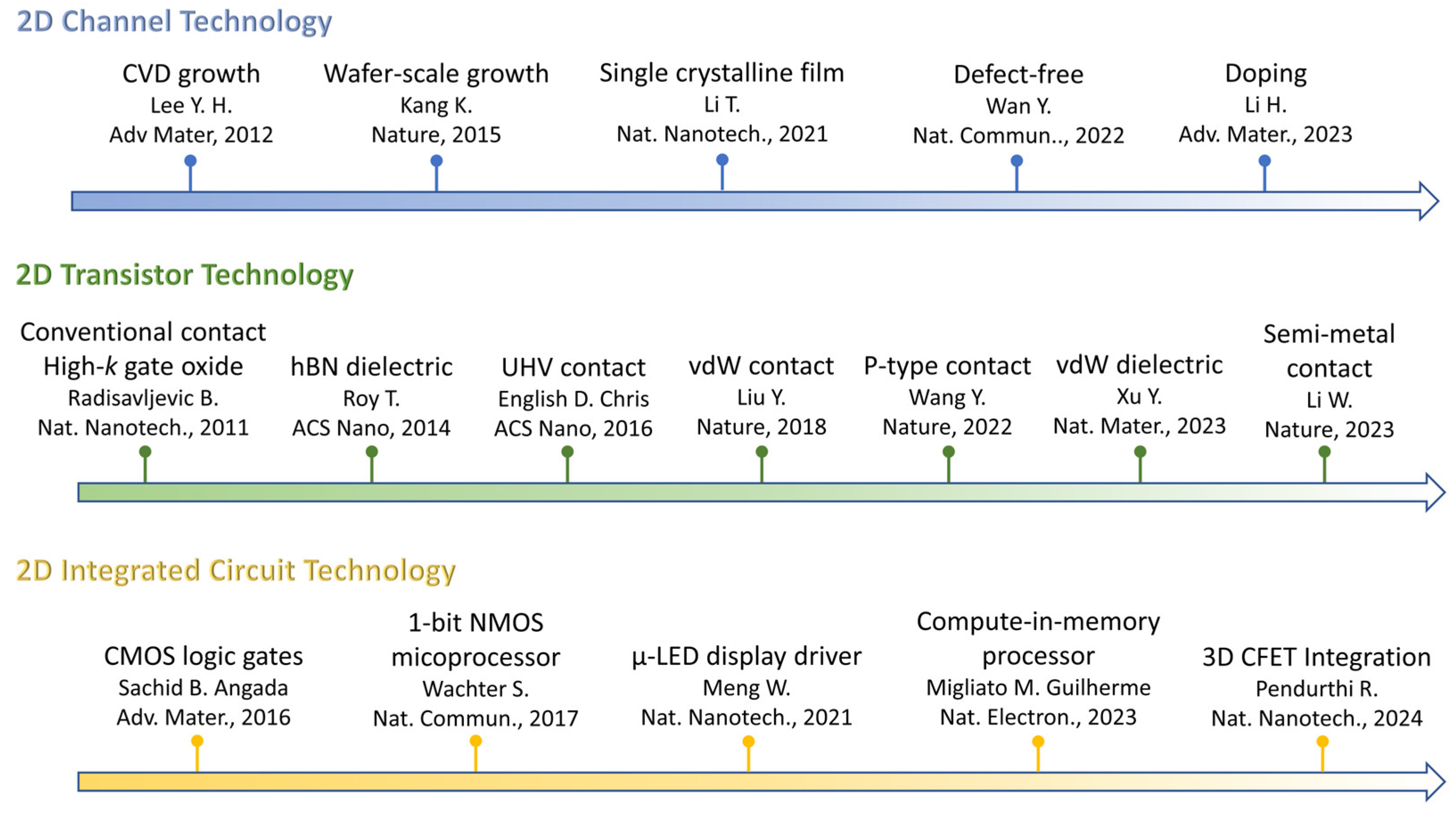
:1. Introduction
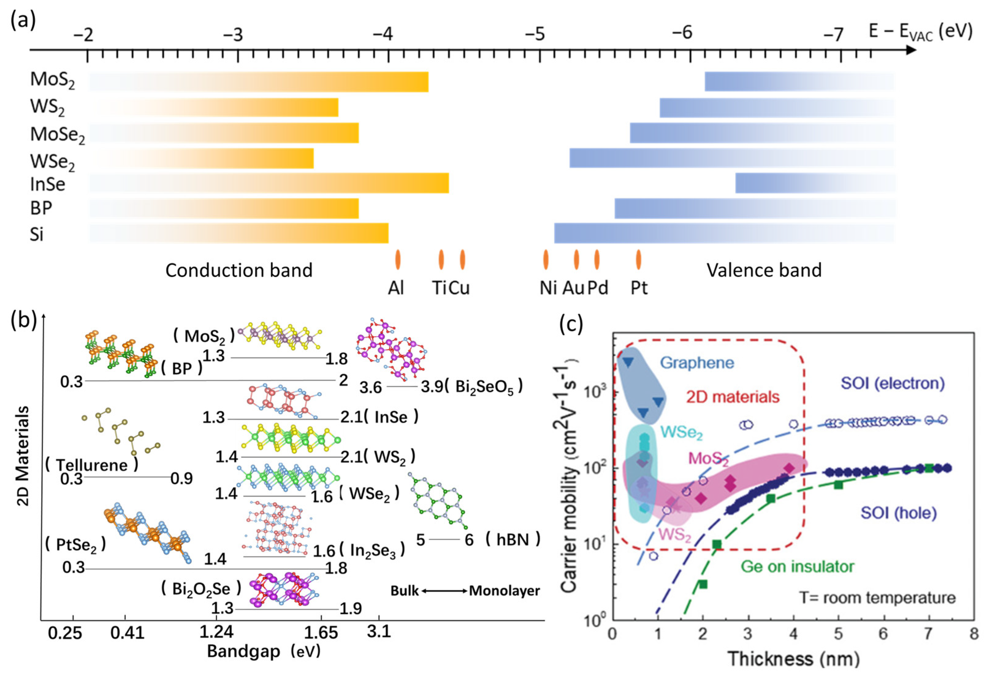
2. Two-Dimensional Semiconductor Materials for Transistor Technology
3. Preparation of Wafer-Scale 2D Semiconductor Films
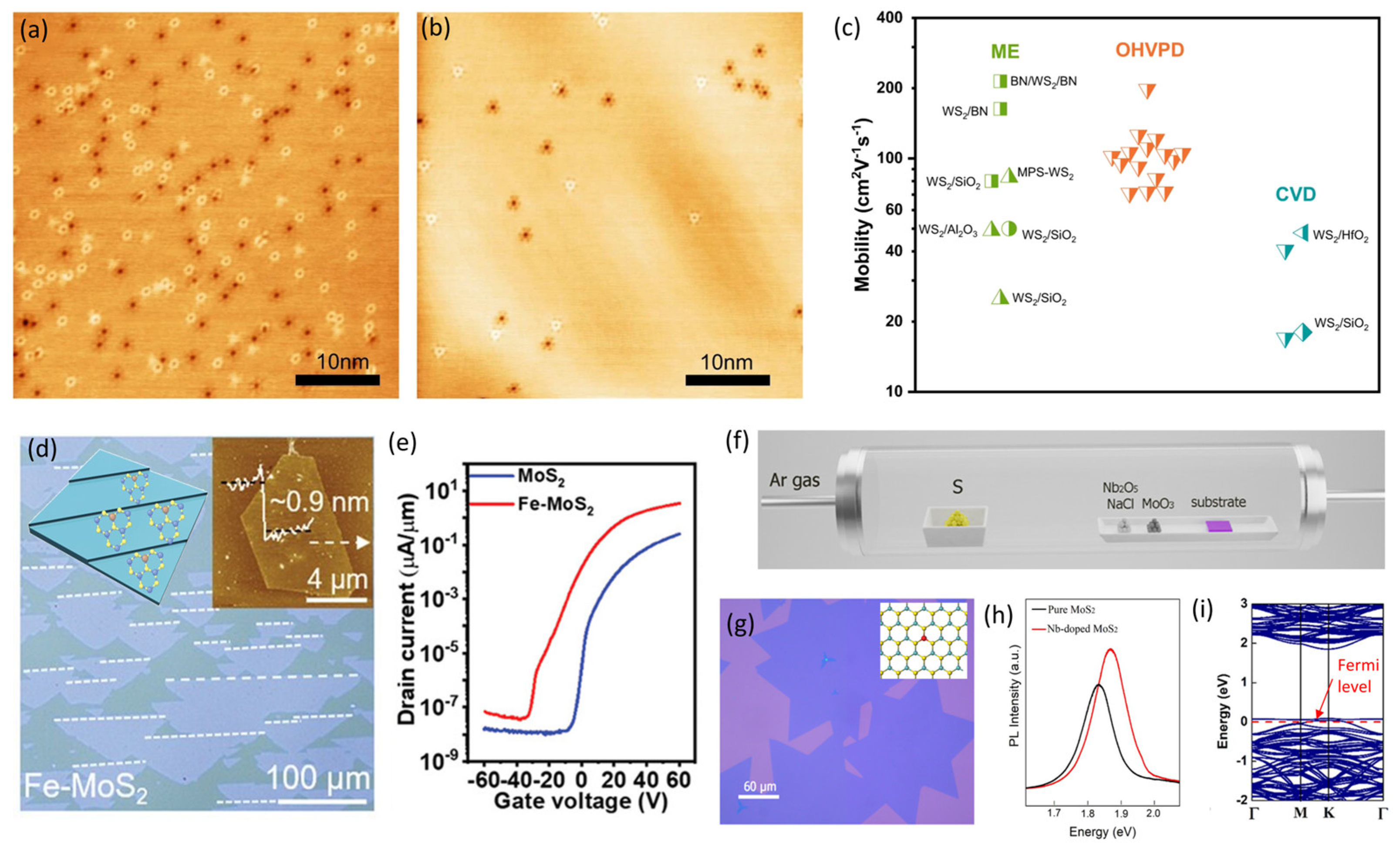
3.1. Controlled Synthesis of 2D Semiconductor Films
3.2. Defect Control and Doping Techniques
4. Two-Dimensional Semiconductor-Based Complementary Transistors
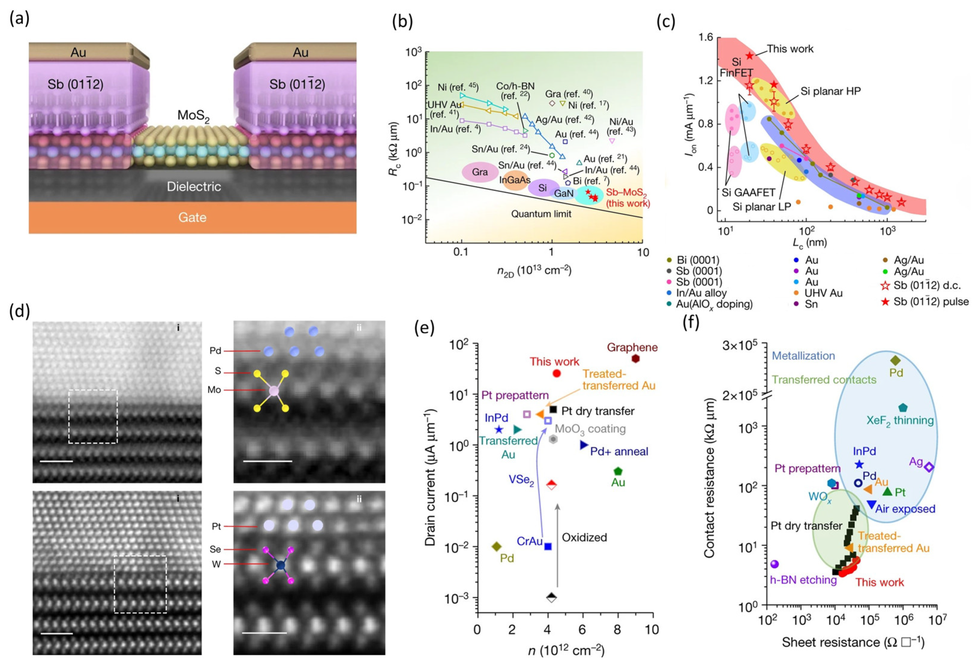
4.1. Towards Low-Resistance Ohmic Contact
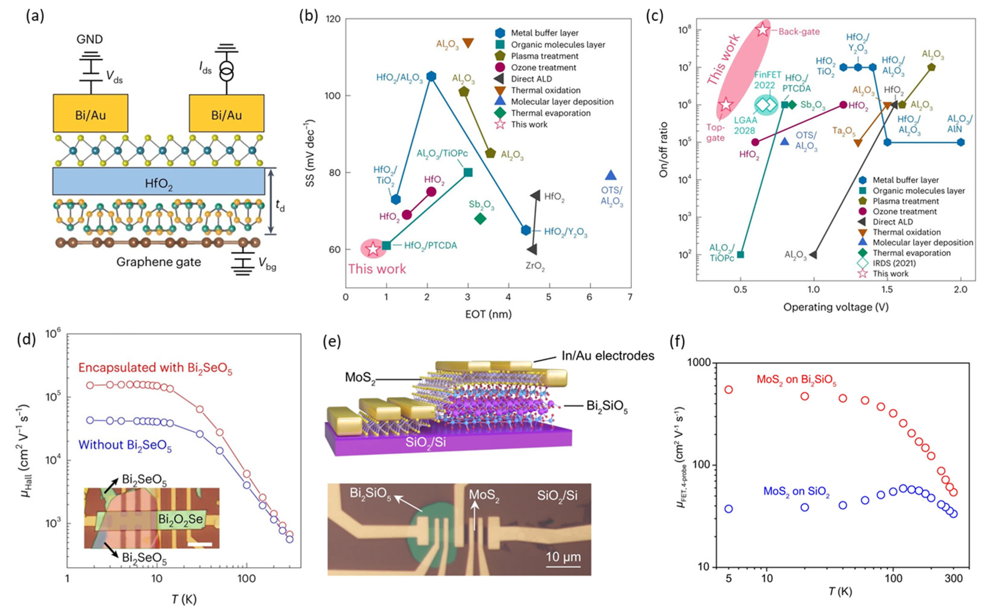
4.2. High-κ Gate Dielectrics Strategies
5. Two-Dimensional Semiconductors for Post-Moore Transistors and Circuits
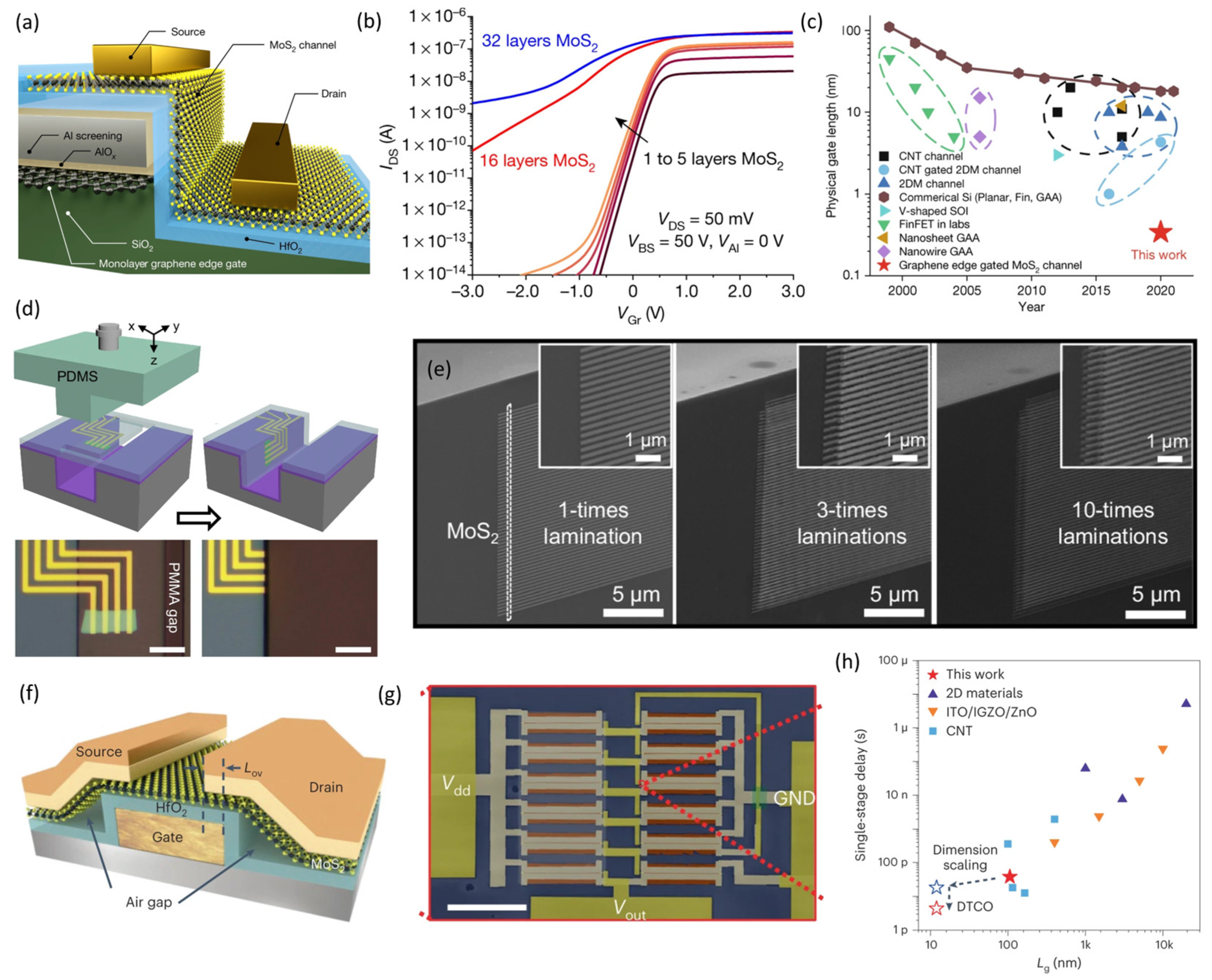
5.1. Two-Dimensional FETs with Extremely Short Channels
5.2. Functional Circuit Integration
6. Conclusions
Author Contributions
Funding
Data Availability Statement
Conflicts of Interest
References
- Lundstrom, M. Moore’s Law Forever? Science 2003, 299, 210–211. [Google Scholar] [CrossRef] [PubMed]
- Bohr, M. A 30 Year Retrospective on Dennard’s MOSFET Scaling Paper. IEEE Solid-State Circuits Soc. Newsl. 2007, 12, 11–13. [Google Scholar] [CrossRef]
- Akinwande, D.; Huyghebaert, C.; Wang, C.-H.; Serna, M.I.; Goossens, S.; Li, L.-J.; Wong, H.-S.P.; Koppens, F.H.L. Graphene and Two-Dimensional Materials for Silicon Technology. Nature 2019, 573, 507–518. [Google Scholar] [CrossRef] [PubMed]
- Shen, Y.; Dong, Z.; Sun, Y.; Guo, H.; Wu, F.; Li, X.; Tang, J.; Liu, J.; Wu, X.; Tian, H.; et al. The Trend of 2D Transistors toward Integrated Circuits: Scaling Down and New Mechanisms. Adv. Mater. 2022, 34, 2201916. [Google Scholar] [CrossRef]
- Wang, S.; Liu, X.; Zhou, P. The Road for 2D Semiconductors in the Silicon Age. Adv. Mater. 2022, 34, 2106886. [Google Scholar] [CrossRef] [PubMed]
- Chhowalla, M.; Jena, D.; Zhang, H. Two-Dimensional Semiconductors for Transistors. Nat. Rev. Mater. 2016, 1, 16052. [Google Scholar] [CrossRef]
- Novoselov, K.S.; Geim, A.K.; Morozov, S.V.; Jiang, D.; Zhang, Y.; Dubonos, S.V.; Grigorieva, I.V.; Firsov, A.A. Electric Field Effect in Atomically Thin Carbon Films. Science 2004, 306, 666–669. [Google Scholar] [CrossRef]
- Radisavljevic, B.; Radenovic, A.; Brivio, J.; Giacometti, V.; Kis, A. Single-Layer MoS2 Transistors. Nat. Nanotechnol. 2011, 6, 147–150. [Google Scholar] [CrossRef]
- Allain, A.; Kis, A. Electron and Hole Mobilities in Single-Layer WSe2. ACS Nano 2014, 8, 7180–7185. [Google Scholar] [CrossRef]
- Li, L.; Yu, Y.; Ye, G.J.; Ge, Q.; Ou, X.; Wu, H.; Feng, D.; Chen, X.H.; Zhang, Y. Black Phosphorus Field-Effect Transistors. Nat. Nanotechnol. 2014, 9, 372–377. [Google Scholar] [CrossRef]
- Sucharitakul, S.; Goble, N.J.; Kumar, U.R.; Sankar, R.; Bogorad, Z.A.; Chou, F.-C.; Chen, Y.-T.; Gao, X.P.A. Intrinsic Electron Mobility Exceeding 103 cm2/(Vs) in Multilayer InSe FETs. Nano Lett. 2015, 15, 3815–3819. [Google Scholar] [CrossRef]
- Desai, S.B.; Madhvapathy, S.R.; Sachid, A.B.; Llinas, J.P.; Wang, Q.; Ahn, G.H.; Pitner, G.; Kim, M.J.; Bokor, J.; Hu, C.; et al. MoS2 Transistors with 1-Nanometer Gate Lengths. Science 2016, 354, 99–102. [Google Scholar] [CrossRef]
- Yeh, C.-H.; Liang, Z.-Y.; Lin, Y.-C.; Chen, H.-C.; Fan, T.; Ma, C.-H.; Chu, Y.-H.; Suenaga, K.; Chiu, P.-W. Graphene–Transition Metal Dichalcogenide Heterojunctions for Scalable and Low-Power Complementary Integrated Circuits. ACS Nano 2020, 14, 985–992. [Google Scholar] [CrossRef]
- Wang, J.; Guo, X.; Yu, Z.; Ma, Z.; Liu, Y.; Lin, Z.; Chan, M.; Zhu, Y.; Wang, X.; Chai, Y. Low-Power Complementary Inverter with Negative Capacitance 2D Semiconductor Transistors. Adv. Funct. Mater. 2020, 30, 2003859. [Google Scholar] [CrossRef]
- Fan, D.; Li, W.; Qiu, H.; Xu, Y.; Gao, S.; Liu, L.; Li, T.; Huang, F.; Mao, Y.; Zhou, W.; et al. Two-Dimensional Semiconductor Integrated Circuits Operating at Gigahertz Frequencies. Nat. Electron. 2023, 6, 879–887. [Google Scholar] [CrossRef]
- Novoselov, K.S.; Mishchenko, A.; Carvalho, A.; Castro Neto, A.H. 2D Materials and van Der Waals Heterostructures. Science 2016, 353, aac9439. [Google Scholar] [CrossRef] [PubMed]
- Shin, G.H.; Park, C.; Lee, K.J.; Jin, H.J.; Choi, S.-Y. Ultrasensitive Phototransistor Based on WSe2–MoS2 van Der Waals Heterojunction. Nano Lett. 2020, 20, 5741–5748. [Google Scholar] [CrossRef] [PubMed]
- Liu, Y.; Guo, J.; Zhu, E.; Liao, L.; Lee, S.-J.; Ding, M.; Shakir, I.; Gambin, V.; Huang, Y.; Duan, X. Approaching the Schottky–Mott Limit in van Der Waals Metal–Semiconductor Junctions. Nature 2018, 557, 696–700. [Google Scholar] [CrossRef]
- Cui, X.; Lee, G.-H.; Kim, Y.D.; Arefe, G.; Huang, P.Y.; Lee, C.-H.; Chenet, D.A.; Zhang, X.; Wang, L.; Ye, F.; et al. Multi-Terminal Transport Measurements of MoS2 Using a van Der Waals Heterostructure Device Platform. Nat. Nanotechnol. 2015, 10, 534–540. [Google Scholar] [CrossRef]
- Ma, J.; Liu, H.; Yang, N.; Zou, J.; Lin, S.; Zhang, Y.; Zhang, X.; Guo, J.; Wang, H. Circuit-Level Memory Technologies and Applications Based on 2D Materials. Adv. Mater. 2022, 34, 2202371. [Google Scholar] [CrossRef]
- Chung, Y.-Y.; Yun, W.-S.; Chou, B.-J.; Hsu, C.-F.; Yu, S.-M.; Arutchelvan, G.; Li, M.-Y.; Lee, T.-E.; Lin, B.-J.; Li, C.-Y.; et al. Monolayer-MoS2 Stacked Nanosheet Channel with C-Type Metal Contact. In Proceedings of the 2023 International Electron Devices Meeting (IEDM), San Francisco, CA, USA, 9 December 2023; IEEE: New York, NY, USA, 2023; pp. 1–4. [Google Scholar]
- Chung, Y.-Y.; Chou, B.-J.; Hsu, C.-F.; Yun, W.-S.; Li, M.-Y.; Su, S.-K.; Liao, Y.-T.; Lee, M.-C.; Huang, G.-W.; Liew, S.-L.; et al. First Demonstration of GAA Monolayer-MoS2 Nanosheet NFET with 410μA/μm ID 1V VD at 40nm Gate Length. In Proceedings of the 2022 International Electron Devices Meeting (IEDM), San Francisco, CA, USA, 3–7 December 2022; pp. 34.5.1–34.5.4. [Google Scholar]
- Wu, F.; Tian, H.; Shen, Y.; Hou, Z.; Ren, J.; Gou, G.; Sun, Y.; Yang, Y.; Ren, T.-L. Vertical MoS2 Transistors with Sub-1-Nm Gate Lengths. Nature 2022, 603, 259–264. [Google Scholar] [CrossRef]
- Hitesh, S.; Dasika, P.; Watanabe, K.; Taniguchi, T.; Majumdar, K. Integration of 3-Level MoS2 Multibridge Channel FET with 2D Layered Contact and Gate Dielectric. IEEE Electron. Device Lett. 2022, 43, 1993–1996. [Google Scholar] [CrossRef]
- IEEE. International Roadmap for Devices and Systems (IRDSTM). 2022 Edition: More Moore. Available online: https://irds.ieee.org/editions/2022/more-moore (accessed on 2 March 2024).
- Tong, L.; Wan, J.; Xiao, K.; Liu, J.; Ma, J.; Guo, X.; Zhou, L.; Chen, X.; Xia, Y.; Dai, S.; et al. Heterogeneous Complementary Field-Effect Transistors Based on Silicon and Molybdenum Disulfide. Nat. Electron. 2023, 6, 37–44. [Google Scholar] [CrossRef]
- Lemme, M.C.; Akinwande, D.; Huyghebaert, C.; Stampfer, C. 2D Materials for Future Heterogeneous Electronics. Nat. Commun. 2022, 13, 1392. [Google Scholar] [CrossRef]
- Meng, W.; Xu, F.; Yu, Z.; Tao, T.; Shao, L.; Liu, L.; Li, T.; Wen, K.; Wang, J.; He, L.; et al. Three-Dimensional Monolithic Micro-LED Display Driven by Atomically Thin Transistor Matrix. Nat. Nanotechnol. 2021, 16, 1231–1236. [Google Scholar] [CrossRef]
- Zhu, J.; Park, J.-H.; Vitale, S.A.; Ge, W.; Jung, G.S.; Wang, J.; Mohamed, M.; Zhang, T.; Ashok, M.; Xue, M.; et al. Low-Thermal-Budget Synthesis of Monolayer Molybdenum Disulfide for Silicon Back-End-of-Line Integration on a 200 μm Platform. Nat. Nanotechnol. 2023, 18, 456–463. [Google Scholar] [CrossRef]
- Wang, Q.; Li, N.; Tang, J.; Zhu, J.; Zhang, Q.; Jia, Q.; Lu, Y.; Wei, Z.; Yu, H.; Zhao, Y.; et al. Wafer-Scale Highly Oriented Monolayer MoS2 with Large Domain Sizes. Nano Lett. 2020, 20, 7193–7199. [Google Scholar] [CrossRef]
- Wachter, S.; Polyushkin, D.K.; Bethge, O.; Mueller, T. A Microprocessor Based on a Two-Dimensional Semiconductor. Nat. Commun. 2017, 8, 14948. [Google Scholar] [CrossRef] [PubMed]
- Migliato Marega, G.; Ji, H.G.; Wang, Z.; Pasquale, G.; Tripathi, M.; Radenovic, A.; Kis, A. A Large-Scale Integrated Vector–Matrix Multiplication Processor Based on Monolayer Molybdenum Disulfide Memories. Nat. Electron. 2023, 6, 991–998. [Google Scholar] [CrossRef]
- Li, W.; Gong, X.; Yu, Z.; Ma, L.; Sun, W.; Gao, S.; Köroğlu, Ç.; Wang, W.; Liu, L.; Li, T.; et al. Approaching the Quantum Limit in Two-Dimensional Semiconductor Contacts. Nature 2023, 613, 274–279. [Google Scholar] [CrossRef]
- Wang, Y.; Kim, J.C.; Li, Y.; Ma, K.Y.; Hong, S.; Kim, M.; Shin, H.S.; Jeong, H.Y.; Chhowalla, M. P-Type Electrical Contacts for 2D Transition-Metal Dichalcogenides. Nature 2022, 610, 61–66. [Google Scholar] [CrossRef]
- Xiong, X.; Liu, S.; Liu, H.; Chen, Y.; Shi, X.; Wang, X.; Li, X.; Huang, R.; Wu, Y. Top-Gate CVD WSe2 PFETs with Record-High Id ~594 μA/μm, Gm ~244 μS/μm and WSe2/MoS2 CFET Based Half-Adder Circuit Using Monolithic 3D Integration. In Proceedings of the 2022 International Electron Devices Meeting (IEDM), San Francisco, CA, USA, 3 December 2022; IEEE: New York, NY, USA, 2022; pp. 20.6.1–20.6.4. [Google Scholar]
- Xu, Y.; Liu, T.; Liu, K.; Zhao, Y.; Liu, L.; Li, P.; Nie, A.; Liu, L.; Yu, J.; Feng, X.; et al. Scalable Integration of Hybrid High-κ Dielectric Materials on Two-Dimensional Semiconductors. Nat. Mater. 2023, 22, 1078–1084. [Google Scholar] [CrossRef]
- Huang, J.-K.; Wan, Y.; Shi, J.; Zhang, J.; Wang, Z.; Wang, W.; Yang, N.; Liu, Y.; Lin, C.-H.; Guan, X.; et al. High-κ Perovskite Membranes as Insulators for Two-Dimensional Transistors. Nature 2022, 605, 262–267. [Google Scholar] [CrossRef] [PubMed]
- Lee, Y.-H.; Zhang, X.-Q.; Zhang, W.; Chang, M.-T.; Lin, C.-T.; Chang, K.-D.; Yu, Y.-C.; Wang, J.T.-W.; Chang, C.-S.; Li, L.-J.; et al. Synthesis of Large-Area MoS2 Atomic Layers with Chemical Vapor Deposition. Adv. Mater. 2012, 24, 2320–2325. [Google Scholar] [CrossRef]
- Kang, K.; Xie, S.; Huang, L.; Han, Y.; Huang, P.Y.; Mak, K.F.; Kim, C.-J.; Muller, D.; Park, J. High-Mobility Three-Atom-Thick Semiconducting Films with Wafer-Scale Homogeneity. Nature 2015, 520, 656–660. [Google Scholar] [CrossRef]
- Li, T.; Guo, W.; Ma, L.; Li, W.; Yu, Z.; Han, Z.; Gao, S.; Liu, L.; Fan, D.; Wang, Z.; et al. Epitaxial Growth of Wafer-Scale Molybdenum Disulfide Semiconductor Single Crystals on Sapphire. Nat. Nanotechnol. 2021, 16, 1201–1207. [Google Scholar] [CrossRef] [PubMed]
- Wan, Y.; Li, E.; Yu, Z.; Huang, J.-K.; Li, M.-Y.; Chou, A.-S.; Lee, Y.-T.; Lee, C.-J.; Hsu, H.-C.; Zhan, Q.; et al. Low-Defect-Density WS2 by Hydroxide Vapor Phase Deposition. Nat. Commun. 2022, 13, 4149. [Google Scholar] [CrossRef] [PubMed]
- Li, H.; Yang, J.; Li, X.; Luo, Q.; Cheng, M.; Feng, W.; Du, R.; Wang, Y.; Song, L.; Wen, X.; et al. Bridging Synthesis and Controllable Doping of Monolayer 4 in. Length Transition-Metal Dichalcogenides Single Crystals with High Electron Mobility. Adv. Mater. 2023, 35, 2211536. [Google Scholar] [CrossRef]
- Roy, T.; Tosun, M.; Kang, J.S.; Sachid, A.B.; Desai, S.B.; Hettick, M.; Hu, C.C.; Javey, A. Field-Effect Transistors Built from All Two-Dimensional Material Components. ACS Nano 2014, 8, 6259–6264. [Google Scholar] [CrossRef]
- English, C.D.; Shine, G.; Dorgan, V.E.; Saraswat, K.C.; Pop, E. Improved Contacts to MoS2 Transistors by Ultra-High Vacuum Metal Deposition. Nano Lett. 2016, 16, 3824–3830. [Google Scholar] [CrossRef]
- Sachid, A.B.; Tosun, M.; Desai, S.B.; Hsu, C.-Y.; Lien, D.-H.; Madhvapathy, S.R.; Chen, Y.-Z.; Hettick, M.; Kang, J.S.; Zeng, Y.; et al. Monolithic 3D CMOS Using Layered Semiconductors. Adv. Mater. 2016, 28, 2547–2554. [Google Scholar] [CrossRef]
- Pendurthi, R.; Sakib, N.U.; Sadaf, M.U.K.; Zhang, Z.; Sun, Y.; Chen, C.; Jayachandran, D.; Oberoi, A.; Ghosh, S.; Kumari, S.; et al. Monolithic Three-Dimensional Integration of Complementary Two-Dimensional Field-Effect Transistors. Nat. Nanotechnol. 2024, 19, 970–977. [Google Scholar] [CrossRef]
- Chaves, A.; Azadani, J.G.; Alsalman, H.; da Costa, D.R.; Frisenda, R.; Chaves, A.J.; Song, S.H.; Kim, Y.D.; He, D.; Zhou, J.; et al. Bandgap Engineering of Two-Dimensional Semiconductor Materials. NPJ. 2D Mater. Appl. 2020, 4, 29. [Google Scholar] [CrossRef]
- Kang, J.; Zhang, L.; Wei, S.-H. A Unified Understanding of the Thickness-Dependent Bandgap Transition in Hexagonal Two-Dimensional Semiconductors. J. Phys. Chem. Lett. 2016, 7, 597–602. [Google Scholar] [CrossRef] [PubMed]
- Sun, Y.; Luo, S.; Zhao, X.-G.; Biswas, K.; Li, S.-L.; Zhang, L. InSe: A Two-Dimensional Material with Strong Interlayer Coupling. Nanoscale 2018, 10, 7991–7998. [Google Scholar] [CrossRef] [PubMed]
- Tran, V.; Soklaski, R.; Liang, Y.; Yang, L. Layer-Controlled Band Gap and Anisotropic Excitons in Few-Layer Black Phosphorus. Phys. Rev. B 2014, 89, 235319. [Google Scholar] [CrossRef]
- Peng, Z.; Chen, X.; Fan, Y.; Srolovitz, D.J.; Lei, D. Strain Engineering of 2D Semiconductors and Graphene: From Strain Fields to Band-Structure Tuning and Photonic Applications. Light. Sci. Appl. 2020, 9, 190. [Google Scholar] [CrossRef]
- Ma, N.; Jena, D. Charge Scattering and Mobility in Atomically Thin Semiconductors. Phys. Rev. X 2014, 4, 11043. [Google Scholar] [CrossRef]
- Zhang, C.; Wang, R.; Mishra, H.; Liu, Y. Two-Dimensional Semiconductors with High Intrinsic Carrier Mobility at Room Temperature. Phys. Rev. Lett. 2023, 130, 87001. [Google Scholar] [CrossRef]
- Wang, J.; Yao, Q.; Huang, C.-W.; Zou, X.; Liao, L.; Chen, S.; Fan, Z.; Zhang, K.; Wu, W.; Xiao, X.; et al. High Mobility MoS2 Transistor with Low Schottky Barrier Contact by Using Atomic Thick h-BN as a Tunneling Layer. Adv. Mater. 2016, 28, 8302–8308. [Google Scholar] [CrossRef]
- Lin, M.-W.; Kravchenko, I.I.; Fowlkes, J.; Li, X.; Puretzky, A.A.; Rouleau, C.M.; Geohegan, D.B.; Xiao, K. Thickness-Dependent Charge Transport in Few-Layer MoS2 Field-Effect Transistors. Nanotechnology 2016, 27, 165203. [Google Scholar] [CrossRef] [PubMed]
- Li, H.; Cheng, M.; Wang, P.; Du, R.; Song, L.; He, J.; Shi, J. Reducing Contact Resistance and Boosting Device Performance of Monolayer MoS2 by In Situ Fe Doping. Adv. Mater. 2022, 34, 2200885. [Google Scholar] [CrossRef] [PubMed]
- Xu, X.; Guo, T.; Kim, H.; Hota, M.K.; Alsaadi, R.S.; Lanza, M.; Zhang, X.; Alshareef, H.N. Growth of 2D Materials at the Wafer Scale. Adv. Mater. 2022, 34, 2108258. [Google Scholar] [CrossRef]
- Li, X.; Yang, J.; Sun, H.; Huang, L.; Li, H.; Shi, J. Controlled Synthesis and Accurate Doping of Wafer-Scale 2D Semiconducting Transition Metal Dichalcogenides. Adv. Mater. 2023, 2305115. [Google Scholar] [CrossRef]
- Cai, J.; Han, X.; Wang, X.; Meng, X. Atomic Layer Deposition of Two-Dimensional Layered Materials: Processes, Growth Mechanisms, and Characteristics. Matter 2020, 2, 587–630. [Google Scholar] [CrossRef]
- Fu, D.; Zhao, X.; Zhang, Y.-Y.; Li, L.; Xu, H.; Jang, A.-R.; Yoon, S.I.; Song, P.; Poh, S.M.; Ren, T.; et al. Molecular Beam Epitaxy of Highly Crystalline Monolayer Molybdenum Disulfide on Hexagonal Boron Nitride. J. Am. Chem. Soc. 2017, 139, 9392–9400. [Google Scholar] [CrossRef]
- Hussain, S.; Khan, M.F.; Shehzad, M.A.; Vikraman, D.; Iqbal, M.Z.; Choi, D.-C.; Song, W.; An, K.-S.; Seo, Y.; Eom, J.; et al. Layer-Modulated, Wafer Scale and Continuous Ultra-Thin WS2 Films Grown by RF Sputtering via Post-Deposition Annealing. J. Mater. Chem. C Mater. 2016, 4, 7846–7852. [Google Scholar] [CrossRef]
- Serna, M.I.; Yoo, S.H.; Moreno, S.; Xi, Y.; Oviedo, J.P.; Choi, H.; Alshareef, H.N.; Kim, M.J.; Minary-Jolandan, M.; Quevedo-Lopez, M.A. Large-Area Deposition of MoS2 by Pulsed Laser Deposition with In Situ Thickness Control. ACS Nano 2016, 10, 6054–6061. [Google Scholar] [CrossRef]
- Lin, Z.; Liu, Y.; Halim, U.; Ding, M.; Liu, Y.; Wang, Y.; Jia, C.; Chen, P.; Duan, X.; Wang, C.; et al. Solution-Processable 2D Semiconductors for High-Performance Large-Area Electronics. Nature 2018, 562, 254–258. [Google Scholar] [CrossRef]
- Hu, K.-M.; Guo, W.; Deng, X.-L.; Li, X.-Y.; Tu, E.-Q.; Xin, Y.-H.; Xue, Z.-Y.; Jiang, X.-S.; Wang, G.; Meng, G.; et al. Deterministically Self-Assembled 2D Materials and Electronics. Matter 2023, 6, 1654–1668. [Google Scholar] [CrossRef]
- Kwon, J.; Seol, M.; Yoo, J.; Ryu, H.; Ko, D.-S.; Lee, M.-H.; Lee, E.K.; Yoo, M.S.; Lee, G.-H.; Shin, H.-J.; et al. 200-mm-Wafer-Scale Integration of Polycrystalline Molybdenum Disulfide Transistors. Nat. Electron. 2024, 7, 356–364. [Google Scholar] [CrossRef]
- Liu, L.; Li, T.; Ma, L.; Li, W.; Gao, S.; Sun, W.; Dong, R.; Zou, X.; Fan, D.; Shao, L.; et al. Uniform Nucleation and Epitaxy of Bilayer Molybdenum Disulfide on Sapphire. Nature 2022, 605, 69–75. [Google Scholar] [CrossRef] [PubMed]
- Xia, Y.; Chen, X.; Wei, J.; Wang, S.; Chen, S.; Wu, S.; Ji, M.; Sun, Z.; Xu, Z.; Bao, W.; et al. 12-Inch Growth of Uniform MoS2 Monolayer for Integrated Circuit Manufacture. Nat. Mater. 2023, 22, 1324–1331. [Google Scholar] [CrossRef]
- Seol, M.; Lee, M.-H.; Kim, H.; Shin, K.W.; Cho, Y.; Jeon, I.; Jeong, M.; Lee, H.-I.; Park, J.; Shin, H.-J. High-Throughput Growth of Wafer-Scale Monolayer Transition Metal Dichalcogenide via Vertical Ostwald Ripening. Adv. Mater. 2020, 32, 2003542. [Google Scholar] [CrossRef]
- Lei, J.; Xie, Y.; Kutana, A.; Bets, K.V.; Yakobson, B.I. Salt-Assisted MoS2 Growth: Molecular Mechanisms from the First Principles. J. Am. Chem. Soc. 2022, 144, 7497–7503. [Google Scholar] [CrossRef] [PubMed]
- Li, S. Salt-Assisted Chemical Vapor Deposition of Two-Dimensional Transition Metal Dichalcogenides. iScience 2021, 24, 103229. [Google Scholar] [CrossRef]
- Liu, C.; Wang, L.; Qi, J.; Liu, K. Designed Growth of Large-Size 2D Single Crystals. Adv. Mater. 2020, 32, 2000046. [Google Scholar] [CrossRef]
- Zhang, Z.; Huang, Z.; Li, J.; Wang, D.; Lin, Y.; Yang, X.; Liu, H.; Liu, S.; Wang, Y.; Li, B.; et al. Endoepitaxial Growth of Monolayer Mosaic Heterostructures. Nat. Nanotechnol. 2022, 17, 493–499. [Google Scholar] [CrossRef] [PubMed]
- Zhu, J.; Xu, H.; Zou, G.; Zhang, W.; Chai, R.; Choi, J.; Wu, J.; Liu, H.; Shen, G.; Fan, H. MoS2–OH Bilayer-Mediated Growth of Inch-Sized Monolayer MoS2 on Arbitrary Substrates. J. Am. Chem. Soc. 2019, 141, 5392–5401. [Google Scholar] [CrossRef]
- Chen, J.; Tang, W.; Tian, B.; Liu, B.; Zhao, X.; Liu, Y.; Ren, T.; Liu, W.; Geng, D.; Jeong, H.Y.; et al. Chemical Vapor Deposition of High-Quality Large-Sized MoS2 Crystals on Silicon Dioxide Substrates. Adv. Sci. 2016, 3, 1500033. [Google Scholar] [CrossRef]
- Chen, J.; Zhao, X.; Tan, S.J.R.; Xu, H.; Wu, B.; Liu, B.; Fu, D.; Fu, W.; Geng, D.; Liu, Y.; et al. Chemical Vapor Deposition of Large-Size Monolayer MoSe2 Crystals on Molten Glass. J. Am. Chem. Soc. 2017, 139, 1073–1076. [Google Scholar] [CrossRef]
- Rong, Y.; Fan, Y.; Leen Koh, A.; Robertson, A.W.; He, K.; Wang, S.; Tan, H.; Sinclair, R.; Warner, J.H. Controlling Sulphur Precursor Addition for Large Single Crystal Domains of WS2. Nanoscale 2014, 6, 12096–12103. [Google Scholar] [CrossRef]
- Yang, T.; Zheng, B.; Wang, Z.; Xu, T.; Pan, C.; Zou, J.; Zhang, X.; Qi, Z.; Liu, H.; Feng, Y.; et al. Van Der Waals Epitaxial Growth and Optoelectronics of Large-Scale WSe2/SnS2 Vertical Bilayer p–n Junctions. Nat. Commun. 2017, 8, 1906. [Google Scholar] [CrossRef]
- Kim, K.S.; Lee, D.; Chang, C.S.; Seo, S.; Hu, Y.; Cha, S.; Kim, H.; Shin, J.; Lee, J.-H.; Lee, S.; et al. Non-Epitaxial Single-Crystal 2D Material Growth by Geometric Confinement. Nature 2023, 614, 88–94. [Google Scholar] [CrossRef]
- Wang, L.; Xu, X.; Zhang, L.; Qiao, R.; Wu, M.; Wang, Z.; Zhang, S.; Liang, J.; Zhang, Z.; Zhang, Z.; et al. Epitaxial Growth of a 100-Square-Centimetre Single-Crystal Hexagonal Boron Nitride Monolayer on Copper. Nature 2019, 570, 91–95. [Google Scholar] [CrossRef]
- Chen, T.-A.; Chuu, C.-P.; Tseng, C.-C.; Wen, C.-K.; Wong, H.-S.P.; Pan, S.; Li, R.; Chao, T.-A.; Chueh, W.-C.; Zhang, Y.; et al. Wafer-Scale Single-Crystal Hexagonal Boron Nitride Monolayers on Cu (111). Nature 2020, 579, 219–223. [Google Scholar] [CrossRef]
- Yang, P.; Zhang, S.; Pan, S.; Tang, B.; Liang, Y.; Zhao, X.; Zhang, Z.; Shi, J.; Huan, Y.; Shi, Y.; et al. Epitaxial Growth of Centimeter-Scale Single-Crystal MoS2 Monolayer on Au(111). ACS Nano 2020, 14, 5036–5045. [Google Scholar] [CrossRef]
- Kim, J.; Ju, X.; Ang, K.-W.; Chi, D. Van Der Waals Layer Transfer of 2D Materials for Monolithic 3D Electronic System Integration: Review and Outlook. ACS Nano 2023, 17, 1831–1844. [Google Scholar] [CrossRef]
- Choi, S.H.; Kim, H.-J.; Song, B.; Kim, Y.I.; Han, G.; Nguyen, H.T.T.; Ko, H.; Boandoh, S.; Choi, J.H.; Oh, C.S.; et al. Epitaxial Single-Crystal Growth of Transition Metal Dichalcogenide Monolayers via the Atomic Sawtooth Au Surface. Adv. Mater. 2021, 33, 2006601. [Google Scholar] [CrossRef]
- Wang, J.; Xu, X.; Cheng, T.; Gu, L.; Qiao, R.; Liang, Z.; Ding, D.; Hong, H.; Zheng, P.; Zhang, Z.; et al. Dual-Coupling-Guided Epitaxial Growth of Wafer-Scale Single-Crystal WS2 Monolayer on Vicinal a-Plane Sapphire. Nat. Nanotechnol. 2022, 17, 33–38. [Google Scholar] [CrossRef]
- Choi, S.H.; Yang, S.-H.; Park, S.; Cho, B.W.; Nguyen, T.D.; Kim, J.H.; Kim, Y.-M.; Kim, K.K.; Lee, Y.H. Is Chemical Vapor Deposition of Monolayer WSe2 Comparable to Other Synthetic Routes? APL Mater. 2023, 11, 111124. [Google Scholar] [CrossRef]
- Wang, S.; Robertson, A.; Warner, J.H. Atomic Structure of Defects and Dopants in 2D Layered Transition Metal Dichalcogenides. Chem. Soc. Rev. 2018, 47, 6764–6794. [Google Scholar] [CrossRef]
- Zuo, Y.; Liu, C.; Ding, L.; Qiao, R.; Tian, J.; Liu, C.; Wang, Q.; Xue, G.; You, Y.; Guo, Q.; et al. Robust Growth of Two-Dimensional Metal Dichalcogenides and Their Alloys by Active Chalcogen Monomer Supply. Nat. Commun. 2022, 13, 1007. [Google Scholar] [CrossRef] [PubMed]
- Xue, G.; Sui, X.; Yin, P.; Zhou, Z.; Li, X.; Cheng, Y.; Guo, Q.; Zhang, S.; Wen, Y.; Zuo, Y.; et al. Modularized Batch Production of 12-Inch Transition Metal Dichalcogenides by Local Element Supply. Sci. Bull. 2023, 68, 1514–1521. [Google Scholar] [CrossRef] [PubMed]
- Feng, S.; Tan, J.; Zhao, S.; Zhang, S.; Khan, U.; Tang, L.; Zou, X.; Lin, J.; Cheng, H.-M.; Liu, B. Synthesis of Ultrahigh-Quality Monolayer Molybdenum Disulfide through In Situ Defect Healing with Thiol Molecules. Small 2020, 16, 2003357. [Google Scholar] [CrossRef] [PubMed]
- Lin, Y.-C.; Jariwala, B.; Bersch, B.M.; Xu, K.; Nie, Y.; Wang, B.; Eichfeld, S.M.; Zhang, X.; Choudhury, T.H.; Pan, Y.; et al. Realizing Large-Scale, Electronic-Grade Two-Dimensional Semiconductors. ACS Nano 2018, 12, 965–975. [Google Scholar] [CrossRef] [PubMed]
- Lee, D.; Lee, J.J.; Kim, Y.S.; Kim, Y.H.; Kim, J.C.; Huh, W.; Lee, J.; Park, S.; Jeong, H.Y.; Kim, Y.D.; et al. Remote Modulation Doping in van Der Waals Heterostructure Transistors. Nat. Electron. 2021, 4, 664–670. [Google Scholar] [CrossRef]
- Tang, L.; Xu, R.; Tan, J.; Luo, Y.; Zou, J.; Zhang, Z.; Zhang, R.; Zhao, Y.; Lin, J.; Zou, X.; et al. Modulating Electronic Structure of Monolayer Transition Metal Dichalcogenides by Substitutional Nb-Doping. Adv. Funct. Mater. 2021, 31, 2006941. [Google Scholar] [CrossRef]
- Resta, G.V.; Balaji, Y.; Lin, D.; Radu, I.P.; Catthoor, F.; Gaillardon, P.-E.; De Micheli, G. Doping-Free Complementary Logic Gates Enabled by Two-Dimensional Polarity-Controllable Transistors. ACS Nano 2018, 12, 7039–7047. [Google Scholar] [CrossRef]
- Lan, H.-Y.; Tripathi, R.; Liu, X.; Appenzeller, J.; Chen, Z. Wafer-Scale CVD Monolayer WSe2 p-FETs with Record-High 727 μA/μm Ion and 490 μS/μm gmax via Hybrid Charge Transfer and Molecular Doping. In Proceedings of the 2023 International Electron Devices Meeting (IEDM), San Francisco, CA, USA, 9 December 2023; IEEE: New York, NY, USA, 2023; pp. 1–4. [Google Scholar]
- Li, M.; Yao, J.; Wu, X.; Zhang, S.; Xing, B.; Niu, X.; Yan, X.; Yu, Y.; Liu, Y.; Wang, Y. P-Type Doping in Large-Area Monolayer MoS2 by Chemical Vapor Deposition. ACS Appl. Mater. Interfaces 2020, 12, 6276–6282. [Google Scholar] [CrossRef] [PubMed]
- Pandey, S.K.; Alsalman, H.; Azadani, J.G.; Izquierdo, N.; Low, T.; Campbell, S.A. Controlled P-Type Substitutional Doping in Large-Area Monolayer WSe2 Crystals Grown by Chemical Vapor Deposition. Nanoscale 2018, 10, 21374–21385. [Google Scholar] [CrossRef]
- Ma, Z.; Zhang, L.; Zhou, C.; Chan, M. High Current Nb-Doped P-Channel MoS₂ Field-Effect Transistor Using Pt Contact. IEEE Electron Device Lett. 2021, 42, 343–346. [Google Scholar] [CrossRef]
- Sotthewes, K.; van Bremen, R.; Dollekamp, E.; Boulogne, T.; Nowakowski, K.; Kas, D.; Zandvliet, H.J.W.; Bampoulis, P. Universal Fermi-Level Pinning in Transition-Metal Dichalcogenides. J. Phys. Chem. C 2019, 123, 5411–5420. [Google Scholar] [CrossRef] [PubMed]
- Wang, X.; Hu, Y.; Kim, S.Y.; Cho, K.; Wallace, R.M. Mechanism of Fermi Level Pinning for Metal Contacts on Molybdenum Dichalcogenide. ACS Appl. Mater. Interfaces 2024, 16, 13258–13266. [Google Scholar] [CrossRef]
- Kong, L.; Zhang, X.; Tao, Q.; Zhang, M.; Dang, W.; Li, Z.; Feng, L.; Liao, L.; Duan, X.; Liu, Y. Doping-Free Complementary WSe2 Circuit via van Der Waals Metal Integration. Nat. Commun. 2020, 11, 1866. [Google Scholar] [CrossRef] [PubMed]
- Wang, Y.; Chhowalla, M. Making Clean Electrical Contacts on 2D Transition Metal Dichalcogenides. Nat. Rev. Phys. 2022, 4, 101–112. [Google Scholar] [CrossRef]
- Kong, L.; Wu, R.; Chen, Y.; Huangfu, Y.; Liu, L.; Li, W.; Lu, D.; Tao, Q.; Song, W.; Li, W.; et al. Wafer-Scale and Universal van Der Waals Metal Semiconductor Contact. Nat. Commun. 2023, 14, 1014. [Google Scholar] [CrossRef]
- Liu, L.; Kong, L.; Li, Q.; He, C.; Ren, L.; Tao, Q.; Yang, X.; Lin, J.; Zhao, B.; Li, Z.; et al. Transferred van Der Waals Metal Electrodes for Sub-1-nm MoS2 Vertical Transistors. Nat. Electron. 2021, 4, 342–347. [Google Scholar] [CrossRef]
- Tao, Q.; Wu, R.; Zou, X.; Chen, Y.; Li, W.; Lu, Z.; Ma, L.; Kong, L.; Lu, D.; Yang, X.; et al. High-Density Vertical Sidewall MoS2 Transistors through T-Shape Vertical Lamination. Nat. Commun. 2024, 15, 5774. [Google Scholar] [CrossRef]
- Kumar, A.; Schauble, K.; Neilson, K.M.; Tang, A.; Ramesh, P.; Wong, H.-S.P.; Pop, E.; Saraswat, K. Sub-200 Ω·µm Alloyed Contacts to Synthetic Monolayer MoS2. In Proceedings of the 2021 IEEE International Electron Devices Meeting (IEDM), San Francisco, CA, USA, 11–16 December 2021; pp. 7.3.1–7.3.4. [Google Scholar]
- Shen, P.-C.; Su, C.; Lin, Y.; Chou, A.-S.; Cheng, C.-C.; Park, J.-H.; Chiu, M.-H.; Lu, A.-Y.; Tang, H.-L.; Tavakoli, M.M.; et al. Ultralow Contact Resistance between Semimetal and Monolayer Semiconductors. Nature 2021, 593, 211–217. [Google Scholar] [CrossRef]
- Chou, A.-S.; Cheng, C.-C.; Liew, S.-L.; Ho, P.-H.; Wang, S.-Y.; Chang, Y.-C.; Chang, C.-K.; Su, Y.-C.; Huang, Z.-D.; Fu, F.-Y.; et al. High On-State Current in Chemical Vapor Deposited Monolayer MoS2 NFETs With Sn Ohmic Contacts. IEEE Electron. Device Lett. 2021, 42, 272–275. [Google Scholar] [CrossRef]
- Ahmed, F.; Lee, D.; Liu, X.; Qu, D.; Ryu, J.; Yoo, W.J.; Yang, Z. P-Type Polar Transition of Chemically Doped Multilayer MoS2 Transistor. Adv. Mater. 2016, 28, 2345–2351. [Google Scholar] [CrossRef]
- Zeng, Y.; Yin, S.; Jin, W.; Hu, Y.; Wu, S.; Guo, Z.; Lu, J.; Wang, S.; Zhou, G.; Wang, W.; et al. High-Performance p-Type MoS2 Field-Effect Transistor by Toroidal-Magnetic-Field Controlled Oxygen Plasma Doping. 2D Mater. 2019, 6, 025007. [Google Scholar] [CrossRef]
- Ma, Z.; Estrada, C.J.; Gong, K.; Zhang, L.; Chan, M. On-Chip Integrated High Gain Complementary MoS2 Inverter Circuit with Exceptional High Hole Current P-Channel Field-Effect Transistors. Adv. Electron. Mater. 2022, 8, 2200480. [Google Scholar] [CrossRef]
- Li, W.; Zhou, J.; Cai, S.; Yu, Z.; Zhang, J.; Fang, N.; Li, T.; Wu, Y.; Chen, T.; Xie, X.; et al. Uniform and Ultrathin High-κ Gate Dielectrics for Two-Dimensional Electronic Devices. Nat. Electron. 2019, 2, 563–571. [Google Scholar] [CrossRef]
- Bandurin, D.A.; Tyurnina, A.V.; Yu, G.L.; Mishchenko, A.; Zólyomi, V.; Morozov, S.V.; Kumar, R.K.; Gorbachev, R.V.; Kudrynskyi, Z.R.; Pezzini, S.; et al. High Electron Mobility, Quantum Hall Effect and Anomalous Optical Response in Atomically Thin InSe. Nat. Nanotechnol. 2017, 12, 223–227. [Google Scholar] [CrossRef]
- Yang, F.; Zhang, Z.; Wang, N.Z.; Ye, G.J.; Lou, W.; Zhou, X.; Watanabe, K.; Taniguchi, T.; Chang, K.; Chen, X.H.; et al. Quantum Hall Effect in Electron-Doped Black Phosphorus Field-Effect Transistors. Nano Lett. 2018, 18, 6611–6616. [Google Scholar] [CrossRef]
- Knobloch, T.; Illarionov, Y.Y.; Ducry, F.; Schleich, C.; Wachter, S.; Watanabe, K.; Taniguchi, T.; Mueller, T.; Waltl, M.; Lanza, M.; et al. The Performance Limits of Hexagonal Boron Nitride as an Insulator for Scaled CMOS Devices Based on Two-Dimensional Materials. Nat. Electron. 2021, 4, 98–108. [Google Scholar] [CrossRef]
- Ma, Z.; Prawoto, C.; Ahmed, Z.; Xiao, Y.; Zhang, L.; Zhou, C.; Chan, M. Control of Hexagonal Boron Nitride Dielectric Thickness by Single Layer Etching. J. Mater. Chem. C Mater. 2019, 7, 6273–6278. [Google Scholar] [CrossRef]
- Liu, H.; Ye, P.D. MoS2 Dual-Gate MOSFET With Atomic-Layer-Deposited Al2O2 as Top-Gate Dielectric. IEEE Electron Device Lett. 2012, 33, 546–548. [Google Scholar] [CrossRef]
- Lin, D.; Wu, X.; Cott, D.; Verreck, D.; Groven, B.; Sergeant, S.; Smets, Q.; Sutar, S.; Asselberghs, I.; Radu, I. Dual Gate Synthetic WS2 MOSFETs with 120μS/μm Gm 2.7μF/cm2 Capacitance and Ambipolar Channel. In Proceedings of the 2020 IEEE International Electron Devices Meeting (IEDM), San Francisco, CA, USA, 12–18 December 2020; pp. 3.6.1–3.6.4. [Google Scholar]
- Wang, X.; Zhang, T.-B.; Yang, W.; Zhu, H.; Chen, L.; Sun, Q.-Q.; Zhang, D.W. Improved Integration of Ultra-Thin High- κ Dielectrics in Few-Layer MoS2 FET by Remote Forming Gas Plasma Pretreatment. Appl. Phys. Lett. 2017, 110, 053110. [Google Scholar] [CrossRef]
- Park, J.H.; Fathipour, S.; Kwak, I.; Sardashti, K.; Ahles, C.F.; Wolf, S.F.; Edmonds, M.; Vishwanath, S.; Xing, H.G.; Fullerton-Shirey, S.K.; et al. Atomic Layer Deposition of Al2O3 on WSe2 Functionalized by Titanyl Phthalocyanine. ACS Nano 2016, 10, 6888–6896. [Google Scholar] [CrossRef]
- Zhang, C.; Tu, T.; Wang, J.; Zhu, Y.; Tan, C.; Chen, L.; Wu, M.; Zhu, R.; Liu, Y.; Fu, H.; et al. Single-Crystalline van Der Waals Layered Dielectric with High Dielectric Constant. Nat. Mater. 2023, 22, 832–837. [Google Scholar] [CrossRef] [PubMed]
- Tan, C.; Yu, M.; Tang, J.; Gao, X.; Yin, Y.; Zhang, Y.; Wang, J.; Gao, X.; Zhang, C.; Zhou, X.; et al. 2D Fin Field-Effect Transistors Integrated with Epitaxial High- κ Gate Oxide. Nature 2023, 616, 66–72. [Google Scholar] [CrossRef] [PubMed]
- Chen, J.; Liu, Z.; Dong, X.; Gao, Z.; Lin, Y.; He, Y.; Duan, Y.; Cheng, T.; Zhou, Z.; Fu, H.; et al. Vertically Grown Ultrathin Bi2SiO2 as High-κ Single-Crystalline Gate Dielectric. Nat. Commun. 2023, 14, 4406. [Google Scholar] [CrossRef]
- Xiong, X.; Tong, A.; Wang, X.; Liu, S.; Li, X.; Huang, R.; Wu, Y. Demonstration of Vertically-Stacked CVD Monolayer Channels: MoS2 Nanosheets GAA-FET with Ion > 700 μA/μm and MoS2/WSe2 CFET. In Proceedings of the 2021 IEEE International Electron Devices Meeting (IEDM), San Francisco, CA, USA, 16 December 2021; pp. 7.5.1–7.5.4. [Google Scholar]
- Huang, X.; Liu, C.; Tang, Z.; Zeng, S.; Liu, L.; Hou, X.; Chen, H.; Li, J.; Jiang, Y.-G.; Zhang, D.W.; et al. High Drive and Low Leakage Current MBC FET with Channel Thickness 1.2nm/0.6nm. In Proceedings of the 2020 IEEE International Electron Devices Meeting (IEDM), San Francisco, CA, USA, 12–18 December 2020; pp. 12.1.1–12.1.4. [Google Scholar]
- Jayachandran, D.; Pendurthi, R.; Sadaf, M.U.K.; Sakib, N.U.; Pannone, A.; Chen, C.; Han, Y.; Trainor, N.; Kumari, S.; Mc Knight, T.V.; et al. Three-Dimensional Integration of Two-Dimensional Field-Effect Transistors. Nature 2024, 625, 276–281. [Google Scholar] [CrossRef]
- Ning, H.; Yu, Z.; Li, T.; Shen, H.; Long, G.; Shi, Y.; Wang, X. From Lab to Fab: Path Forward for 2D Material Electronics. Sci. China Inf. Sci. 2023, 66, 160411. [Google Scholar] [CrossRef]
- Estrada, C.J.; Ma, Z.; Chan, M. Complementary Two-Dimensional (2-D) FET Technology with MoS2/HBN/Graphene Stack. IEEE Electron Device Lett. 2021, 42, 1890–1893. [Google Scholar] [CrossRef]
- Guo, Y.; Li, J.; Zhan, X.; Wang, C.; Li, M.; Zhang, B.; Wang, Z.; Liu, Y.; Yang, K.; Wang, H.; et al. Van Der Waals Polarity-Engineered 3D Integration of 2D Complementary Logic. Nature 2024, 630, 346–352. [Google Scholar] [CrossRef]
- Chen, L.; Li, S.; Feng, X.; Wang, L.; Huang, X.; Tee, B.C.-K.; Ang, K.-W. Gigahertz Integrated Circuits Based on Complementary Black Phosphorus Transistors. Adv. Electron. Mater. 2018, 4, 1800274. [Google Scholar] [CrossRef]
- Li, N.; Wang, Q.; Shen, C.; Wei, Z.; Yu, H.; Zhao, J.; Lu, X.; Wang, G.; He, C.; Xie, L.; et al. Large-Scale Flexible and Transparent Electronics Based on Monolayer Molybdenum Disulfide Field-Effect Transistors. Nat. Electron. 2020, 3, 711–717. [Google Scholar] [CrossRef]
- Liu, L.; Han, J.; Xu, L.; Zhou, J.; Zhao, C.; Ding, S.; Shi, H.; Xiao, M.; Ding, L.; Ma, Z.; et al. Aligned, High-Density Semiconducting Carbon Nanotube Arrays for High-Performance Electronics. Science 2020, 368, 850–856. [Google Scholar] [CrossRef] [PubMed]
- Zhang, Y.; Li, J.; Zhang, Y.; Yang, H.; Guan, Y.; Chan, M.; Lu, L.; Zhang, S. Deep Sub-Micron Self-Aligned Bottom-Gate Amorphous InGaZnO Thin-Film Transistors with Low-Resistance Source/Drain. IEEE Electron Device Lett. 2023, 44, 1300–1303. [Google Scholar] [CrossRef]
- Kang, S.-H.; Jo, J.-W.; Lee, J.M.; Moon, S.; Shin, S.B.; Bin Choi, S.; Byeon, D.; Kim, J.; Kim, M.-G.; Kim, Y.-H.; et al. Full Integration of Highly Stretchable Inorganic Transistors and Circuits within Molecular-Tailored Elastic Substrates on a Large Scale. Nat. Commun. 2024, 15, 2814. [Google Scholar] [CrossRef] [PubMed]
- Peng, L.-M. High-Performance Carbon Nanotube Thin-Film Transistor Technology. ACS Nano 2023, 17, 22156–22166. [Google Scholar] [CrossRef]
- Estrada, C.J.; Ma, Z.; Chan, M. Complementary Two-Dimensional (2-D) MoS2 FET Technology. In Proceedings of the ESSDERC 2021-IEEE 51st European Solid-State Device Research Conference (ESSDERC), Grenoble, France, 13–22 September 2021; pp. 219–222. [Google Scholar]
- Lu, Y.-C.; Huang, J.-K.; Chao, K.-Y.; Li, L.-J.; Hu, V.P.-H. Projected Performance of Si- and 2D-Material-Based SRAM Circuits Ranging from 16 nm to 1 nm Technology Nodes. Nat. Nanotechnol. 2024, 19, 1066–1072. [Google Scholar] [CrossRef]
- Xie, M.; Jia, Y.; Nie, C.; Liu, Z.; Tang, A.; Fan, S.; Liang, X.; Jiang, L.; He, Z.; Yang, R. Monolithic 3D Integration of 2D Transistors and Vertical RRAMs in 1T–4R Structure for High-Density Memory. Nat. Commun. 2023, 14, 5952. [Google Scholar] [CrossRef]


| Material | Bandgap (eV) | Mobility (cm2V−1s−1) | ION (μA/μm) | On/Off Ratio | Channel Length | Channel Thickness | Integration Scale | Ref. |
|---|---|---|---|---|---|---|---|---|
| Si | 1.12 | 100 | 800 | 105 | 30 nm | 6 nm | 109 cm−2 | [25] |
| IGZO | 3.5 | 13.5 | 10 | 109 | 0.2~10 μm | 10~100 nm | 442 cm−2 | [132,133] |
| CNT | 0.4~0.8 | 104 | 10 | 105 | 5 nm | 1 nm | 104 | [131,134] |
| MoS2 | 1.3~1.8 | 3 | 2 | 108 | 2 μm | 1.3 nm | 115 | [31] |
| 70 | 1230 | 108 | 20 nm | 0.65 nm | 1 | [33] | ||
| / | 0.69 | 105 | 0.34 nm | 0.65 nm | 1 | [23] |
Disclaimer/Publisher’s Note: The statements, opinions and data contained in all publications are solely those of the individual author(s) and contributor(s) and not of MDPI and/or the editor(s). MDPI and/or the editor(s) disclaim responsibility for any injury to people or property resulting from any ideas, methods, instructions or products referred to in the content. |
© 2024 by the authors. Licensee MDPI, Basel, Switzerland. This article is an open access article distributed under the terms and conditions of the Creative Commons Attribution (CC BY) license (https://creativecommons.org/licenses/by/4.0/).
Share and Cite
Liang, M.; Yan, H.; Wazir, N.; Zhou, C.; Ma, Z. Two-Dimensional Semiconductors for State-of-the-Art Complementary Field-Effect Transistors and Integrated Circuits. Nanomaterials 2024, 14, 1408. https://doi.org/10.3390/nano14171408
Liang M, Yan H, Wazir N, Zhou C, Ma Z. Two-Dimensional Semiconductors for State-of-the-Art Complementary Field-Effect Transistors and Integrated Circuits. Nanomaterials. 2024; 14(17):1408. https://doi.org/10.3390/nano14171408
Chicago/Turabian StyleLiang, Meng, Han Yan, Nasrullah Wazir, Changjian Zhou, and Zichao Ma. 2024. "Two-Dimensional Semiconductors for State-of-the-Art Complementary Field-Effect Transistors and Integrated Circuits" Nanomaterials 14, no. 17: 1408. https://doi.org/10.3390/nano14171408