Article

Enhancing the Performance of Nanocrystalline SnO2 for Solar Cells through Photonic Curing Using Impedance Spectroscopy Analysis

by
Moulay Ahmed Slimani
,
Jaime A. Benavides-Guerrero
,
Sylvain G. Cloutier
and
Ricardo Izquierdo
*
Département de Génie Électrique, École de Technologie Supérieure, 1100 Rue Notre-Dame Ouest, Montréal, QC H3C 1K3, Canada
*
Author to whom correspondence should be addressed.
Nanomaterials 2024, 14(18), 1508; https://doi.org/10.3390/nano14181508
Submission received: 20 August 2024 / Revised: 10 September 2024 / Accepted: 14 September 2024 / Published: 17 September 2024
(This article belongs to the Special Issue Photofunctional Nanomaterials and Nanostructures)

Abstract

:
Wide-bandgap tin oxide ( SnO 2 ) thin-films are frequently used as an electron-transporting layers in perovskite solar cells due to their superior thermal and environmental stabilities. However, its crystallization by conventional thermal methods typically requires high temperatures and long periods of time. These post-processing conditions severely limit the choice of substrates and reduce the large-scale manufacturing capabilities. This work describes the intense-pulsed-light-induced crystallization of SnO 2 thin-films using only 500 μ s of exposure time. The thin-films’ properties are investigated using both impedance spectroscopy and photoconductivity characteristic measurements. A Nyquist plot analysis establishes that the process parameters have a significant impact on the electronic and ionic behaviors of the SnO 2 films. Most importantly, we demonstrate that light-induced crystallization yields improved topography and excellent electrical properties through enhanced charge transfer, improved interfacial morphology, and better ohmic contact compared to thermally annealed (TA) SnO 2 films.

1. Introduction

Electron-transporting layers (ETLs) are critical components in most optoelectronic device architectures, including perovskite solar cells (PSCs). These PSC devices rely on organic–inorganic perovskite materials to efficiently absorb light and generate charge carriers [1,2,3]. ETL layers are essential for promoting efficient electron transport, block holes, align energy levels, and ultimately enhance the efficiency and stability of perovskite solar cells. Choosing appropriate ETL materials is essential for the performance of PSCs. Typical ETL materials require processing between 150 and 500 °C, resulting in higher processing times and energy costs. Most importantly, this prevents their integration on most low-cost substrates that require processing temperatures below 150 °C [4,5]. In this context, intense pulsed light annealing, also sometimes referred to as photonic curing (PC) [6], is an emerging technique that is ideally suited for large-scale manufacturing as is relies on short, high-intensity light pulses to anneal materials selectively and rapidly [7,8]. In this process, the optical energy absorbed by the active material can sustain carefully controlled light-induced annealing with minimal substrate damage. As a result, even metals with relatively high melting points can be successfully sintered on low-cost plastic- or paper-based substrates [9,10,11]. As such, this technique is also especially well-suited for roll-to-roll (R2R) manufacturing [12]. SnO 2 metal-oxide thin-films were first utilized as ETLs for perovskite-based solar cells nearly a decade ago [13,14]. They have since emerged as the preferred material for PSCs over TiO 2 and ZnO due to their large band gaps, higher charge mobilities, and better stabilities under ambient conditions [15,16,17]. A few years later, SnO 2 films were photonically annealed in just 20 m s , enabling the fabrication of PSCs with reduced hysteresis and a 15% power conversion efficiency [9]. However, these previous studies did not address the effect of photonic curing on the electronic properties of SnO2 films. To investigate this, we used impedance spectroscopy (IS), which is a rapid technique for evaluating these properties. IS is a powerful tool to shed light on the kinetic processes taking place within electrochemical systems [18,19]. During measurement, a small alternating current (AC) signal is coupled with a direct current (DC) voltage and is applied to the device. The phase difference between the DC voltage and AC current is measured over a wide frequency range to identify the various physical effects in the device. As a result, IS measurements can assess the physical and chemical processes of various types of devices, including optoelectronic devices, fuel cells, and solid-state batteries [20]. IS is a non-destructive [14,21,22] tool that can be effectively used to optimize the stability and performance of these devices by characterizing their charge transport properties [18,23]. Typically, the IS measurements exhibit two arcs corresponding to low-frequency (LF) and high-frequency (HF) responses, respectively [24,25]. The series resistance (Rs), charge-transfer resistance ( R C T ), and parallel capacitance can be determined from the HF and LF responses.
This work explores the impact of the photonic curing parameters on thin-film SnO 2 properties using IS and photocurrent characteristic analysis to unveil and control the ionic and electronic kinetics within the treated SnO 2 layer. As we demonstrate, this improved understanding and control leads to enhanced electronic properties with great potential for improved perovskite solar cell manufacturability.

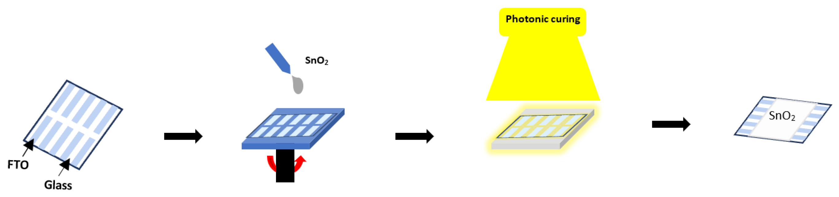
2. Experimental Section

Commercial patterned fluorine-doped tin Oxide (FTO) substrates (SHENZHEN HUAYU UNION TECHNOLOGY, Shenzhen, China, resistance: 7 Ohm/sq) doped with fluorine are cleaned using a sequential process of 10 min each in an ultrasonic bath with DI water, acetone, and isopropyl alcohol (IPA). After drying with a nitrogen spray gun, residual organic contaminants are removed by performing a 15 min O 2 plasma treatment (Plasma Etch, Carson City, NV, USA, PE-100LF). To prepare the SnO 2 solution, a colloidal precursor of SnO 2 obtained from Alfa Aesar (15% in H 2 O colloidal dispersion CN: 044592.A3) is diluted with DI water to a concentration of 3% by volume. The SnO 2 solution is spin-coated onto the clean FTO substrate in one step in air 3000 rpm for 30 s . The edges of the FTO electrodes are then cleaned with a dry cotton swab to enable electrical and IS measurements (Figure 1). For TA, SnO 2 films are annealed using a hot plate at 150 °C for 30 min under ambient air. For photonic curing, each sample is treated using a Novacentrix PulseForge system (500 V /3 A ) power supply with 3 capacitors providing radiant energy greater than 20 J.cm−2 using a lamp system (7.6 c m × 60.8 c m ) with an illumination area of 300 mm × 75 mm. The light source ensures uniform curing over a large area and delivers short (20 μ s to 100 m s ) but intense light pulses from a broadband xenon flash lamp (200–1500 n m ). A Paois (Fluxim AG, SN:20121 Winterthur, Switzerland) tool is used for all electrical and IS measurements. SEM (SU8230 Hitachi) and AFM (Bruker, MultiMode8, Billerica, MA, USA ) are used for topography inspection. For impedance spectroscopy, the FTO edges that are used as electrodes are connected to the Paois to measure the impedance over a range of frequencies (10 Hz to 10 M Hz ) in the dark at 0.07 V perturbation at room temperature. Impedance data can be analyzed using Nyquist and Bode plots to interpret electrochemical properties such as the charge transfer resistance, capacitance, and dielectric properties. The temperature is simulated using NovaCentrix SimPulse software, this simulation package is standard on the PulseForge Version 3, Austin, TX, USA. The configuration is modeled as follows (from bottom to top): aluminum chuck, 6 mm; glass, 2.2 mm; and FTO, 600 nm. The thicknesses of the glass and FTO layers are taken from the manufacturers. X-ray diffraction (XRD) is done using a Bruker D8 Advance (Billerica, MA, USA), and optical absorbance is done using a UV–Vis–NIR spectrophotometer from Perkin Elmer (Waltham, MA, USA).

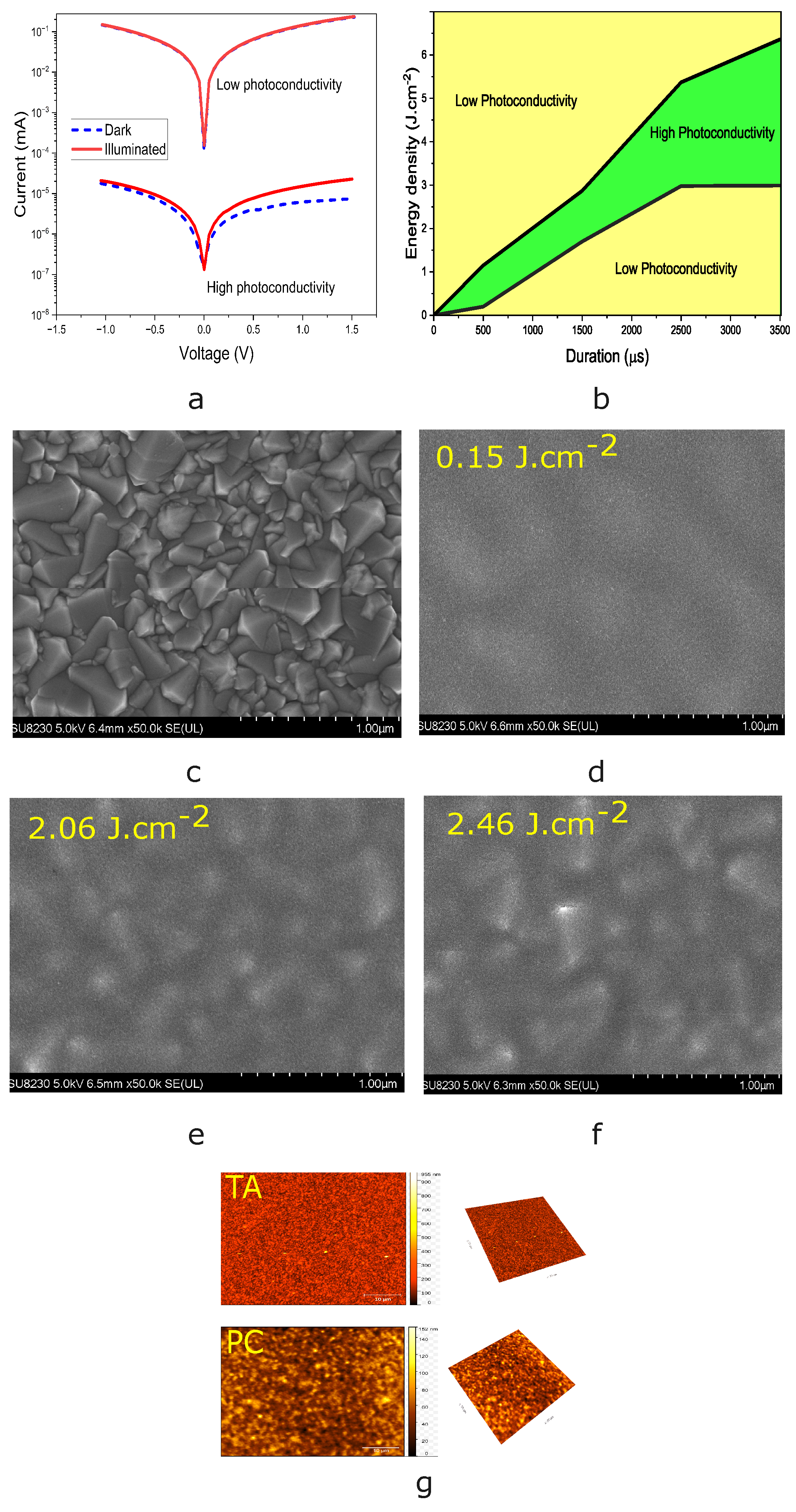
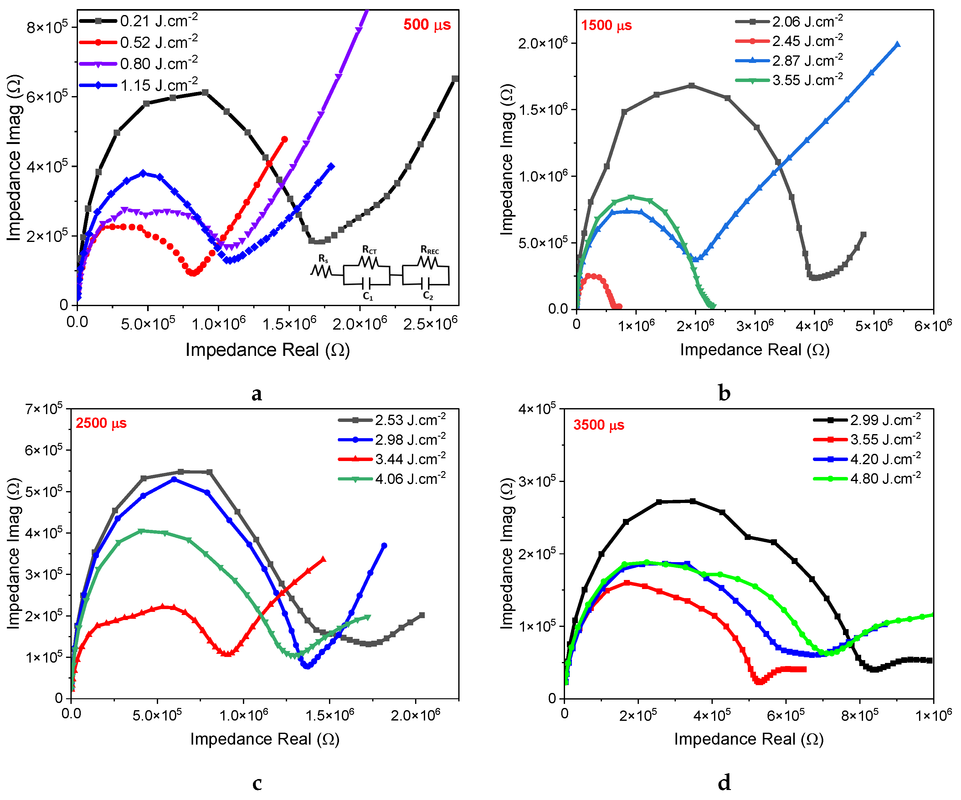
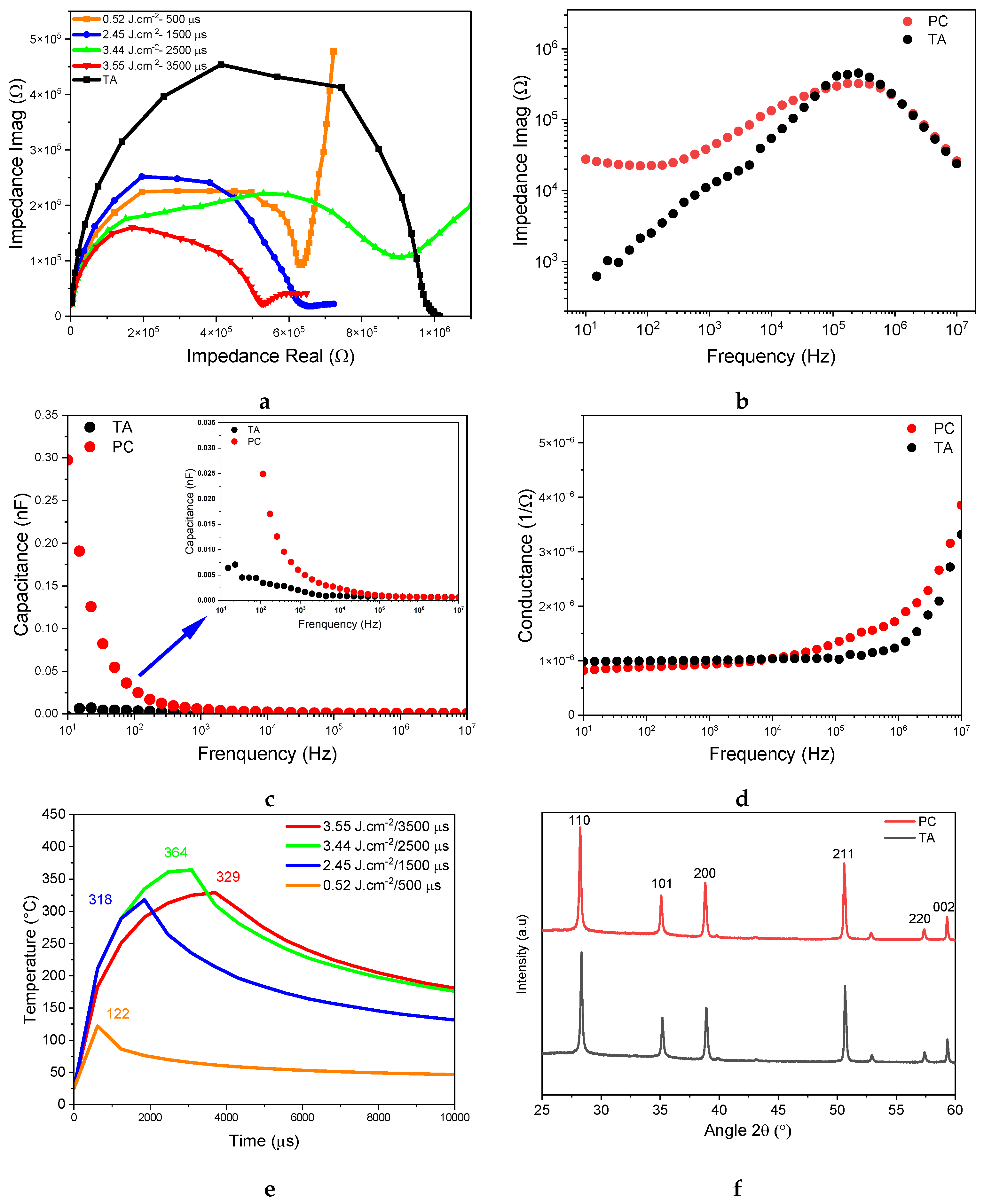
3. Results and Discussion

After deposition of colloidal SnO 2 films using the protocol, samples are post-processed using varying pulse durations and energy densities using the methodology described in the Section 2. To investigate the impact of PC on the electrical properties of SnO 2 films, we conduct flash annealing for pulse durations of 500, 1500, 2500, and 3500 μ s , followed by photocurrent measurements. This allows us to optimize our photonic annealing parameters and define the high photoconductivity range for SnO 2 films. Photocurrent analysis is used to map the different zones’ photoconductivity. Pulses ranging from 500 to 3500 μ s are utilized to complete the photo-responsivity characterization. Figure 2a shows the I–V responses in the dark and under illumination for two samples photonically treated using a pulse duration of 2500 μ s and, respectively, 2 J.cm−2 and 4 J.cm−2. A low photo-responsivity indicates that the illumination and dark curves approach the overlap limit, while a high photo-responsivity indicates a clear offset (more than 0.5 order of magnitude) between the I–V characteristics in the dark and under illumination. Based on such measurements, Figure 2b displays a photo-responsivity map for samples photonically treated using different pulse durations vs. energy densities. To shed light on these results, IS and SEM characterizations are conducted. SnO 2 is highly transparent, which makes photonic curing difficult [26]. To mitigate this problem, we use substrates with FTO patterns that act as a structural support and a stable base for the growth of SnO 2 nanoparticles. This helps promote the transmission of the heat generated when light is absorbed by the nanoparticles [27], which can increase the local temperature around the nanoparticles and promote the recrystallization process. FTO substrates exhibit rougher surfaces than glass [28], promoting superior adhesion and growth of SnO 2 nanoparticles [29]. Their conductivity enhances the electrical properties of the resulting SnO 2 films. The FTO substrate’s roughness directly influences both the diameter and alignment of the SnO 2 nanoparticles [30]. Areas with FTO patterns acting as a blanket allow for changes in nanoparticle recrystallization depending on the energy density used.
Figure 2c displays SEM images of the bare FTO substrate, and Figure 2d–f show SnO 2 films deposited on FTO and photonically treated using energy densities of 0.15, 2.06, and 2.46 J.cm−2, respectively. As the energy density is increased from 0.15 to 2.06 to 2.46 J.cm−2 while using 1500 μ s pulse durations, the SnO 2 -covered films appear increasingly granular, while the distinct grain boundaries that were clearly observed in the FTO/glass film are less apparent. The recrystallization of the SnO 2 film follows the substrate topography well, revealing the underlying FTO grain profile. This process indicates that higher energy densities lead to improved film–substrate adhesion and more pronounced exposure of the underlying grain structure. The photonic curing of SnO 2 wet films enables water evaporation and subsequent crystallization of SnO 2 nanoparticles [31]. The degree of crystallization greatly affects the photoconductivity of SnO 2 films and their ability to carry charge carriers [32,33]. A film’s properties largely depend on two independent parameters: the energy density and the pulse duration of the pulsed light.
To obtain quantitative information and to better understand the surface morphology and roughness, we also conduct AFM analyses on samples subjected to different types of annealing treatments. Figure 2g shows the surface roughness of the film samples for a scan area of 5 × 5 μ m 2 . It highlights the improvement in surface topography after optimal photonic treatment with SnO 2 , with a root-mean-square roughness of 14.01 n m , compared to 45.57 n m for the thermally annealed sample. Roughness is defined as the microscopic and macroscopic variations on a material’s surface [34]. It measures the irregularities present on the surface. These variations can have a significant impact on the physical and chemical properties of materials, such as the recombination rates in ETL films for solar cells. Low-roughness films can reduce the recombination rate and thus improve performance [35]. The morphological effect of PC processing can be beneficial in terms of device performance. This significant improvement underscores another important advantage of photonic treatment for enhancing the quality of SnO 2 as an electron transport layer (ETL) in perovskite solar cells.
This section focuses on the variation of IS results for SnO 2 films treated with different energy densities and pulse durations of 500, 1500, 2500, and 3500 μ s . For these measurements, the SnO 2 film is deposited onto FTO glass, and its electrochemical behavior can be represented by an equivalent circuit that produces a semicircle on the Nyquist diagram. Figure 3a–d displays IS results for SnO 2 samples treated using these different pulse durations and energy densities. When the pulse duration is fixed and the energy density is increased, the semicircle decreases until it reaches its minimum, and then the arc widens. The frequency response exhibits two distinct behaviors. At high frequencies (HF), it is dominated by the resistance attributed to electronic transport ( R C T ). At low frequencies ( L F ), it is dominated by the recombination resistance ( R r e c ) related to ionic diffusion and charge accumulation at the contacts [36,37]. In Figure 3, it corresponds to the second semicircle inclined at 45° to the real axis in the Nyquist graph [38]. The semi-circle in the high-frequency region is generally related to the counter-electrode and its interface [39]. A smaller half-circle suggests a lower R C T and better photoconductivity of the device. These Nyquist plots suggest that our devices’ equivalent circuits can be accurately modeled by a resistor–capacitor (RC) pair in the dark AC regime [40]. As such, the interface contribution can be derived from the equivalent circuit’s parameters [41]. The series resistance (Rs) can be obtained by measuring the shift of the semi-circle from the origin along the horizontal axis [42]. However, the time constant related to the physical phenomena dominating at both the low and high frequencies is described by τ H F . ω H F = 1 and τ L F . ω L F = 1 , with ω H F , L F = 2 π · f m a x , H F , L F [40]. The time constants can be deduced from the IS results by identifying the peak of the semicircle, which corresponds to the maximum frequency, or by calculating τ = R e q . C e q , as shown in Table 1.
Figure 4a compares the Cole–Cole plots for films that are photonically treated using 500, 1500, 2500, and 3500 μ s pulses with respective energy densities of 0.52, 2.45, 3.44, and 3.55 J.cm−2 with a typical film sample crystallized using standard thermal annealing.Clearly, the physical and chemical properties of the resulting SnO 2 films appear greatly affected by the pulse duration and energy density. When the pulse duration is 3500 μ s and the energy density is 3.55 J.cm−2, the high-frequency arc is smallest, suggesting that the film is less resistive and facilitating charge transfer. In comparison, the thermally annealed sample exhibits a larger semicircle than all of the photonically treated samples. This suggests increased imaginary impedance associated with a decrease in charge transfer. Figure 4b–d compare the imaginary impedance, capacitance, and conductance versus the frequency for the best thermally annealed and the best photonically treated films for the conditions 3.55 J.cm−2 and 3500 μ s . In Figure 4b, the high-frequency (HF) peaks appear between 10 5 10 6 Hz for both samples. The response time can be obtained by taking the inverse of the peak frequency from the imaginary impedance graph. Table 1 presents the IS parameters extracted from the spectra. There, the R C T value for the thermally annealed sample is roughly twice the value achieved using optimal photonic curing conditions. This suggests that the SnO 2 /FTO interface provides a low R C T under the effect of photonic annealing, which facilitates charge carrier transport. The resulting time constant is 0.8 μ s for the thermally annealed film, compared to 0.38 μ s for the optimal photonic curing conditions. This suggest that photonically induced crystallization promotes a faster response time, resulting in low recombination and more dominant ionic diffusion behavior [43,44]. At low frequencies, the thermally annealed device does not exhibit any measurable peak, which is consistent with the presence of the single semicircle in Figure 4b. In contrast, the impedance plot of the photonically treated device is curved at low frequencies, explaining the start of the second semicircle in this region. Frequency, time constant, and conductivity values are good indicators of process kinetics [45,46]. Indeed, the dark IS can be directly related to the carrier density, mobility, and conductivity [38]. The temperature simulation results using the photonic annealing parameters shown in Figure 4e reveal a relationship between the energy density, pulse duration, and resulting temperature of the SnO 2 film. As the energy density increases from 0.52 to 3.55 J.cm−2, the temperature increases from 122 to 364 °C then decreases to 329 °C for the film treated with an energy density of 3.55 J.cm−2 and a pulse duration of 3500 μ s . These parameters are crucial to determine the energy transferred to the SnO 2 film, but they show a non-linear trend with temperature. Figure 4f shows X-ray diffraction (XRD) measurements of the thermally and photonically annealed SnO 2 films. The prominent peaks are determined to correspond to (110), (101), (200), (211), (220), and (002), confirming the tetragonal crystal structure of SnO 2 for both the TA and PC films [47,48,49].
Figure 4c,d show capacitance and conductivity evolutions as a function of the operation frequency. Figure 4c illustrates two distinct capacitance behaviors, each corresponding to a specific polarization process. This distinction makes it possible to identify specific capacitive processes directly from the plot [50,51]. The high-frequency capacitance C H F (above 100 k Hz ) exhibits a plateau in the order of 1 p F for both thermally and photonically treated devices and is rather similar for both annealing processes. This region represents the geometric capacitance and is due to the intrinsic dielectric polarization of the SnO 2 layer [50]. However, photonic treatment achieves higher capacitance values at low frequencies (below 1 KHz) compared to the thermally annealed device. This is primarily due to the accumulation of charges or ions [52,53] resulting from the polarization of the interfaces between the SnO 2 layer and the electrodes. At low frequencies, the increase in capacitance is dominated by ionic movement in the dark and electronic movement in the light [54,55]. In circuits that exhibit capacitive behavior, the capacitor offers less resistance to the flow of alternating current as the frequency increases. Accordingly, Figure 4d shows increases in conductance for both devices in the high-frequency region. This behavior is consistent with that of semiconductors, where capacitance and conductance vary inversely [56,57,58].
The optical properties of the prepared samples are characterized by UV–Vis absorption spectra. As shown in Figure 5a, the transmittance of PC-treated films is higher than that of TA-treated films, which is desirable for solar cell applications. SnO 2 is a direct bandgap (BG) semiconductor; its BG can be calculated using a Tauc plot [59], as shown in Figure 5b. The calculated BGs are 3.45 eV and 3.43 eV for the TA- and PC-treated films, respectively, which explains why the TA film is slightly more transparent than the PC film. Measurements in Figure 5c,d compare the dark injection transients for the photocurrent rise and decay for the thermally and photonically treated (3.55 J.cm−2, 3500 μ s ) samples. This time-of-flight technique is useful for determining majority carrier mobility and trapping, especially in thin-films [60]. Figure 5c illustrates that the current for the photonically treated film rises to 2.7 m A , compared to 2.3 m A for the thermally annealed film. The current also increases more rapidly in the photonically treated sample, reflecting the interrelationship between charge carrier generation and recombination. Therefore, the rapid increase in current for the PC sample can be attributed to the fast accumulation of photogenerated carriers [61]. Figure 5d compares the decay of the transient current. After reaching its maximum, the current decay depends on the charge capture coefficient [62]. The decay graph illustrates the speed of charge recombination after being excited by a 1.2 V pulse voltage. A shorter carrier lifetime suggests faster recombination and a high carrier capture rate, which implies more rapid current decay for the thermally annealed sample. In contrast, photonic curing yields a lower recombination rate, resulting in slower decay and longer current holding times. The photogeneration and recombination processes have a significant impact on the density and mobility of charge carriers. Figure 5e compares the charge mobility using the photo-CELIV technique using the following expression [63,64,65]:
μ = 2 d 2 3 A . t m a x 2 ( 1 + 0.36 Δ J m a x )
where d is the SnO 2 film thickness, A is the slope of the extraction voltage ramp, t m a x is the time related to the current peak, and Δ is the difference between the maximum current and the displacement current plateau. Photo-CELIV is a technique used to extract the charge mobility by illuminating the device. The measurement displays the current overshoot and the time at which the current reaches its maximum, which is an essential parameter for quantifying mobility. However, it should be noted that Photo-CELIV only measures fast carriers and cannot distinguish between the mobility of electrons and holes. The Photo-CELIV measurements for the film after optimized photonic treatment yield 4.56 × 10 2 V   c m 2 s 1 , compared with 3.66 × 10 2 V   c m 2 s 1 for the thermally annealed film. This measurement does not precisely reflect the mobility of the SnO 2 material. However, it serves as a characterization for comparing the fastest or maximum carrier mobility values. This higher maximum mobility compared to thermal annealing is consistent with previous results.

4. Conclusions

In summary, we propose an optimized photonic annealing approach to improve the electrical properties of SnO 2 thin-films compared to standard annealing. SnO 2 thin-films play an essential role in emerging device architectures, especially as the electron-transporting layer (ETL) for perovskite-based solar cells. We use impedance spectroscopy to analyze the electrical behavior of SnO 2 films in the dark. The results indicate that the impedance spectroscopy response depends significantly on both the energy density and the pulse duration and shed light on the resulting ionic and electronic transfer. Additionally, we demonstrate that photonic treatment yields SnO 2 layers with enhanced electrical performance and a significantly reduced manufacturing time compared to standard thermal annealing. This would be a great advantage for large-scale manufacturing of better and cheaper perovskite-based solar cells.

Author Contributions

Writing—original draft, methodology, resources, conceptualization, and formal analysis, M.A.S.; simulation and manuscript review, J.A.B.-G.; supervision, visualization, and review and editing, S.G.C. and R.I. All authors have read and agreed to the published version of the manuscript.

Funding

The authors would like to acknowledge the financial support received from the NSERC via Discovery grants RGPIN-2023-05211 and RGPIN 2022-03083 as well as from the Canada Research Chairs (CRC-2021-00490).

Data Availability Statement

The data that support the findings of this study are available from the corresponding author upon reasonable request.

Conflicts of Interest

The authors declare no conflicts of interest.

Abbreviations

The following abbreviations are used in this manuscript:
ETLElectron-transporting layer
PSCPerovskite solar cell
TAThermal annealing
PCPhotonic curing

References

  1. Wei, Z.; Zhao, Y.; Jiang, J.; Yan, W.; Feng, Y.; Ma, J. Research progress on hybrid organic–inorganic perovskites for photo-applications. Chin. Chem. Lett. 2020, 31, 3055–3064. [Google Scholar] [CrossRef]
  2. Jing, H.; Zhu, Y.; Peng, R.W.; Li, C.Y.; Xiong, B.; Wang, Z.; Liu, Y.; Wang, M. Hybrid organic-inorganic perovskite metamaterial for light trapping and photon-to-electron conversion. Nanophotonics 2020, 9, 3323–3333. [Google Scholar] [CrossRef]
  3. Yang, Z.; Lai, J.; Zhu, R.; Tan, J.; Luo, Y.; Ye, S. Electronic Disorder Dominates the Charge-Carrier Dynamics in Two-Dimensional/Three-Dimensional Organic–Inorganic Perovskite Heterostructure. J. Phys. Chem. C 2022, 126, 12689–12695. [Google Scholar] [CrossRef]
  4. Jiang, Q.; Chu, Z.; Wang, P.; Yang, X.; Liu, H.; Wang, Y.; Yin, Z.; Wu, J.; Zhang, X.; You, J. Planar-structure perovskite solar cells with efficiency beyond 21%. Adv. Mater. 2017, 29, 1703852. [Google Scholar] [CrossRef] [PubMed]
  5. Liu, C.; Hu, M.; Zhou, X.; Wu, J.; Zhang, L.; Kong, W.; Li, X.; Zhao, X.; Dai, S.; Xu, B. Efficiency and stability enhancement of perovskite solar cells by introducing CsPbI3 quantum dots as an interface engineering layer. NPG Asia Mater. 2018, 10, 552–561. [Google Scholar] [CrossRef]
  6. Schroder, K.A. Mechanisms of photonic curing™: Processing high temperature films on low temperature substrates. Nanotechnology 2011, 2, 220–223. [Google Scholar]
  7. Akhavan, V.; Schroder, K.; Farnsworth, S. Photonic Curing. Inkjet Print. Ind. Mater. Technol. Syst. Appl. 2022, 2, 1051–1064. [Google Scholar]
  8. Secor, E.B.; Ahn, B.Y.; Gao, T.Z.; Lewis, J.A.; Hersam, M.C. Rapid and versatile photonic annealing of graphene inks for flexible printed electronics. Adv. Mater. 2015, 27, 6683–6688. [Google Scholar] [CrossRef]
  9. Zhu, M.; Liu, W.; Ke, W.; Clark, S.; Secor, E.B.; Song, T.B.; Kanatzidis, M.G.; Li, X.; Hersam, M.C. Millisecond-pulsed photonically-annealed tin oxide electron transport layers for efficient perovskite solar cells. J. Mater. Chem. A 2017, 5, 24110–24115. [Google Scholar] [CrossRef]
  10. Altay, B.N.; Turkani, V.S.; Pekarovicova, A.; Fleming, P.D.; Atashbar, M.Z.; Bolduc, M.; Cloutier, S.G. One-step photonic curing of screen-printed conductive Ni flake electrodes for use in flexible electronics. Sci. Rep. 2021, 11, 3393. [Google Scholar] [CrossRef]
  11. Piper, R.T.; Daunis, T.B.; Xu, W.; Schroder, K.A.; Hsu, J.W. Photonic curing of nickel oxide transport layer and perovskite active layer for flexible perovskite solar cells: A path towards high-throughput manufacturing. Front. Energy Res. 2021, 9, 640960. [Google Scholar] [CrossRef]
  12. Maskey, B.B.; Koirala, G.R.; Kim, Y.; Park, H.; Yadav, P.; Park, J.; Sun, J.; Cho, G. Photonic Curing for Enhancing the Performance of Roll-to-Roll Printed Electronic Devices. Oklahoma State University, USA. 2019. Available online: https://core.ac.uk/reader/215230370 (accessed on 31 July 2024).
  13. Dong, Q.; Shi, Y.; Wang, K.; Li, Y.; Wang, S.; Zhang, H.; Xing, Y.; Du, Y.; Bai, X.; Ma, T. Insight into perovskite solar cells based on SnO2 compact electron-selective layer. J. Phys. Chem. C 2015, 119, 10212–10217. [Google Scholar] [CrossRef]
  14. Matacena, I.; Guerriero, P.; Lancellotti, L.; Alfano, B.; De Maria, A.; La Ferrara, V.; Mercaldo, L.V.; Miglietta, M.L.; Polichetti, T.; Rametta, G. Impedance spectroscopy analysis of perovskite solar cell stability. Energies 2023, 16, 4951. [Google Scholar] [CrossRef]
  15. Hu, M.; Zhang, L.; She, S.; Wu, J.; Zhou, X.; Li, X.; Wang, D.; Miao, J.; Mi, G.; Chen, H. Electron transporting bilayer of SnO2 and TiO2 nanocolloid enables highly efficient planar perovskite solar cells. Sol. RRL 2020, 4, 1900331. [Google Scholar] [CrossRef]
  16. Irfan, M.; Ünlü, F.; Lê, K.; Fischer, T.; Ullah, H.; Mathur, S. Electrospun Networks of ZnO-SnO2 Composite Nanowires as Electron Transport Materials for Perovskite Solar Cells. J. Nanomater. 2022, 2022, 6043406. [Google Scholar] [CrossRef]
  17. Martínez-Denegri, G.; Colodrero, S.; Kramarenko, M.; Martorell, J. All-nanoparticle SnO2/TiO2 electron-transporting layers processed at low temperature for efficient thin-film perovskite solar cells. ACS Appl. Energy Mater. 2018, 1, 5548–5556. [Google Scholar] [CrossRef]
  18. Magar, H.S.; Hassan, R.Y.; Mulchandani, A. Electrochemical impedance spectroscopy (EIS): Principles, construction, and biosensing applications. Sensors 2021, 21, 6578. [Google Scholar] [CrossRef]
  19. Pascoe, A.R.; Duffy, N.W.; Scully, A.D.; Huang, F.; Cheng, Y.B. Insights into planar CH3NH3PbI3 perovskite solar cells using impedance spectroscopy. J. Phys. Chem. C 2015, 119, 4444–4453. [Google Scholar] [CrossRef]
  20. Sinclair, D.C. Characterisation of electro-materials using ac impedance spectroscopy. Boletín Soc. Española Cerámica Vidr. 1995, 34, 55–65. [Google Scholar]
  21. Middlemiss, L.A.; Rennie, A.J.; Sayers, R.; West, A.R. Characterisation of batteries by electrochemical impedance spectroscopy. Energy Rep. 2020, 6, 232–241. [Google Scholar] [CrossRef]
  22. Shohan, S.; Harm, J.; Hasan, M.; Starly, B.; Shirwaiker, R. Non-destructive quality monitoring of 3D printed tissue scaffolds via dielectric impedance spectroscopy and supervised machine learning. Procedia Manuf. 2021, 53, 636–643. [Google Scholar] [CrossRef]
  23. Cherian, C.T.; Zheng, M.; Reddy, M.; Chowdari, B.; Sow, C.H. Zn2SnO4 nanowires versus nanoplates: Electrochemical performance and morphological evolution during Li-cycling. ACS Appl. Mater. Interfaces 2013, 5, 6054–6060. [Google Scholar] [CrossRef] [PubMed]
  24. Suo, Z.; Xiao, Z.; Li, S.; Liu, J.; Xin, Y.; Meng, L.; Liang, H.; Kan, B.; Yao, Z.; Li, C.; et al. Efficient and stable inverted structure organic solar cells utilizing surface-modified SnO2 as the electron transport layer. Nano Energy 2023, 118, 109032. [Google Scholar] [CrossRef]
  25. Dıaz-Flores, L.; Ramırez-Bon, R.; Mendoza-Galvan, A.; Prokhorov, E.; Gonzalez-Hernandez, J. Impedance spectroscopy studies on SnO2 films prepared by the sol–gel process. J. Phys. Chem. Solids 2003, 64, 1037–1042. [Google Scholar] [CrossRef]
  26. Piper, R.T.; Xu, W.; Hsu, J.W. How Optical and Electrical Properties of ITO Coated Willow Glass Affect Photonic Curing Outcome for Upscaling Perovskite Solar Cell Manufacturing. IEEE J. Photovoltaics 2022, 12, 722–727. [Google Scholar] [CrossRef]
  27. Albrecht, A.; Rivadeneyra, A.; Abdellah, A.; Lugli, P.; Salmerón, J.F. Inkjet printing and photonic sintering of silver and copper oxide nanoparticles for ultra-low-cost conductive patterns. J. Mater. Chem. C 2016, 4, 3546–3554. [Google Scholar] [CrossRef]
  28. Pan, D.; Fan, H.; Li, Z.; Wang, S.; Huang, Y.; Jiao, Y.; Yao, H. Influence of substrate on structural properties and photocatalytic activity of TiO2 films. Micro Nano Lett. 2017, 12, 82–86. [Google Scholar] [CrossRef]
  29. Hamdi, M.; Saleh, M.N.; Poulis, J.A. Improving the adhesion strength of polymers: Effect of surface treatments. J. Adhes. Sci. Technol. 2020, 34, 1853–1870. [Google Scholar] [CrossRef]
  30. Bandara, T.; Aththanayake, A.; Kumara, G.; Samarasekara, P.; DeSilva, L.A.; Tennakone, K. Transparent and conductive F-Doped SnO2 nanostructured thin films by sequential nebulizer spray pyrolysis. MRS Adv. 2021, 6, 417–421. [Google Scholar] [CrossRef]
  31. Ghahremani, A.H.; Martin, B.; Gupta, A.; Bahadur, J.; Ankireddy, K.; Druffel, T. Rapid fabrication of perovskite solar cells through intense pulse light annealing of SnO2 and triple cation perovskite thin films. Mater. Des. 2020, 185, 108237. [Google Scholar] [CrossRef]
  32. Mukhamedshina, D.M.; Beisenkhanov, N.B. Influence of crystallization on the properties of SnO2 thin films. In Advances in Crystallization Processes; IntechOpen: London, UK, 2012. [Google Scholar]
  33. Zhu, Z.; Bai, Y.; Liu, X.; Chueh, C.; Yang, S.; Jen, A.K. Enhanced efficiency and stability of inverted perovskite solar cells using highly crystalline SnO2 nanocrystals as the robust electron-transporting layer. Adv. Mater. 2016, 28, 6478–6484. [Google Scholar] [CrossRef] [PubMed]
  34. Creager, S.E.; Hockett, L.A.; Rowe, G.K. Consequences of microscopic surface roughness for molecular self-assembly. Langmuir 1992, 8, 854–861. [Google Scholar] [CrossRef]
  35. Keshtmand, R.; Zamani-Meymian, M.R.; Mohamadkhani, F.; Taghavinia, N. Smoothing and coverage improvement of SnO2 electron transporting layer by NH4F treatment: Enhanced fill factor and efficiency of perovskite solar cells. Sol. Energy 2021, 228, 253–262. [Google Scholar] [CrossRef]
  36. Salado, M.; Contreras-Bernal, L.; Caliò, L.; Todinova, A.; López-Santos, C.; Ahmad, S.; Borras, A.; Idígoras, J.; Anta, J.A. Impact of moisture on efficiency-determining electronic processes in perovskite solar cells. J. Mater. Chem. A 2017, 5, 10917–10927. [Google Scholar] [CrossRef]
  37. Li, N.; Yan, J.; Ai, Y.; Jiang, E.; Lin, L.; Shou, C.; Yan, B.; Sheng, J.; Ye, J. A low-temperature TiO2/SnO2 electron transport layer for high-performance planar perovskite solar cells. Sci. China Mater 2020, 63, 207–215. [Google Scholar] [CrossRef]
  38. Shibuya, H.; Inoue, S.; Ihara, M. Evaluation of dye-sensitized solar cells using forward bias applied impedance spectroscopy under dark. ECS Trans. 2009, 16, 93. [Google Scholar] [CrossRef]
  39. Abdulrahim, S.M.; Ahmad, Z.; Bahadra, J.; Al-Thani, N.J. Electrochemical impedance spectroscopy analysis of hole transporting material free mesoporous and planar perovskite solar cells. Nanomaterials 2020, 10, 1635. [Google Scholar] [CrossRef]
  40. Bredar, A.R.; Chown, A.L.; Burton, A.R.; Farnum, B.H. Electrochemical impedance spectroscopy of metal oxide electrodes for energy applications. ACS Appl. Energy Mater. 2020, 3, 66–98. [Google Scholar] [CrossRef]
  41. Chang, B.Y.; Park, S.M. Integrated description of electrode/electrolyte interfaces based on equivalent circuits and its verification using impedance measurements. Anal. Chem. 2006, 78, 1052–1060. [Google Scholar] [CrossRef]
  42. Matacena, I. Equivalent circuit extraction procedure from Nyquist plots for graphene-silicon solar cells. In Proceedings of the 2019 15th Conference on Ph.D Research in Microelectronics and Electronics (PRIME), Lausanne, Switzerland, 15–18 July 2019; pp. 273–276. [Google Scholar] [CrossRef]
  43. Prochowicz, D.; Trivedi, S.; Parikh, N.; Saliba, M.; Kalam, A.; Mahdi Tavakoli, M.; Yadav, P. In the Quest of Low-Frequency Impedance Spectra of Efficient Perovskite Solar Cells. Energy Technol. 2021, 9, 2100229. [Google Scholar] [CrossRef]
  44. Alvarez, A.O.; Arcas, R.; Aranda, C.A.; Bethencourt, L.; Mas-Marzá, E.; Saliba, M.; Fabregat-Santiago, F. Negative capacitance and inverted hysteresis: Matching features in perovskite solar cells. J. Phys. Chem. Lett. 2020, 11, 8417–8423. [Google Scholar] [CrossRef] [PubMed]
  45. Laschuk, N.O.; Easton, E.B.; Zenkina, O.V. Reducing the resistance for the use of electrochemical impedance spectroscopy analysis in materials chemistry. RSC Adv. 2021, 11, 27925–27936. [Google Scholar] [CrossRef] [PubMed]
  46. Hernández, H.H.; Reynoso, A.R.; González, J.T.; Morán, C.G.; Hernández, J.M.; Ruiz, A.M.; Hernández, J.M.; Cruz, R.O. Electrochemical impedance spectroscopy (EIS): A review study of basic aspects of the corrosion mechanism applied to steels. In Electrochemical Impedance Spectroscopy; IntechOpen: London, UK, 2020; pp. 137–144. [Google Scholar]
  47. Deva Arun Kumar, K.; Valanarasu, S.; Capelle, A.; Nar, S.; Karim, W.; Stolz, A.; Aspe, B.; Semmar, N. Nanostructured Oxide (SnO2, FTO) Thin Films for Energy Harvesting: A Significant Increase in Thermoelectric Power at Low Temperature. Micromachines 2024, 15, 188. [Google Scholar] [CrossRef] [PubMed]
  48. Patil, G.E.; Kajale, D.D.; Gaikwad, V.B.; Jain, G.H. Preparation and characterization of SnO2 nanoparticles by hydrothermal route. Int. Nano Lett. 2012, 2, 17. [Google Scholar] [CrossRef]
  49. Peiris, T.N.; Benitez, J.; Sutherland, L.; Sharma, M.; Michalska, M.; Scully, A.D.; Vak, D.; Gao, M.; Weerasinghe, H.C.; Jasieniak, J. A stable aqueous SnO2 nanoparticle dispersion for roll-to-Roll fabrication of flexible perovskite solar cells. Coatings 2022, 12, 1948. [Google Scholar] [CrossRef]
  50. Guerrero, A.; Garcia-Belmonte, G.; Mora-Sero, I.; Bisquert, J.; Kang, Y.S.; Jacobsson, T.J.; Correa-Baena, J.P.; Hagfeldt, A. Properties of contact and bulk impedances in hybrid lead halide perovskite solar cells including inductive loop elements. J. Phys. Chem. C 2016, 120, 8023–8032. [Google Scholar] [CrossRef]
  51. Almora, O.; Zarazua, I.; Mas-Marza, E.; Mora-Sero, I.; Bisquert, J.; Garcia-Belmonte, G. Capacitive dark currents, hysteresis, and electrode polarization in lead halide perovskite solar cells. J. Phys. Chem. Lett. 2015, 6, 1645–1652. [Google Scholar] [CrossRef]
  52. Mahapatra, A.; Parikh, N.; Kumar, P.; Kumar, M.; Prochowicz, D.; Kalam, A.; Tavakoli, M.M.; Yadav, P. Changes in the electrical characteristics of perovskite solar cells with aging time. Molecules 2020, 25, 2299. [Google Scholar] [CrossRef]
  53. Todinova, A.; Contreras-Bernal, L.; Salado, M.; Ahmad, S.; Morillo, N.; Idígoras, J.; Anta, J.A. Towards a universal approach for the analysis of impedance spectra of perovskite solar cells: Equivalent circuits and empirical analysis. ChemElectroChem 2017, 4, 2891–2901. [Google Scholar] [CrossRef]
  54. Zarazua, I.; Han, G.; Boix, P.P.; Mhaisalkar, S.; Fabregat-Santiago, F.; Mora-Seró, I.; Bisquert, J.; Garcia-Belmonte, G. Surface recombination and collection efficiency in perovskite solar cells from impedance analysis. J. Phys. Chem. Lett. 2016, 7, 5105–5113. [Google Scholar] [CrossRef]
  55. Zarazua, I.; Bisquert, J.; Garcia-Belmonte, G. Light-induced space-charge accumulation zone as photovoltaic mechanism in perovskite solar cells. J. Phys. Chem. Lett. 2016, 7, 525–528. [Google Scholar] [CrossRef] [PubMed]
  56. Li, J.V.; Ferrari, G. Capacitance Spectroscopy of Semiconductors; CRC Press: Boca Raton, FL, USA, 2018. [Google Scholar]
  57. Heeger, A.J.; MacDiarmid, A.G.; Shirakawa, H. The Nobel Prize in Chemistry, 2000: Conductive Polymers; Royal Swedish Academy of Sciences: Stockholm, Sweden, 2000; pp. 1–16. [Google Scholar]
  58. Namsheer, K.; Rout, C.S. Conducting polymers: A comprehensive review on recent advances in synthesis, properties and applications. RSC Adv. 2021, 11, 5659–5697. [Google Scholar]
  59. Wang, Y.; Su, N.; Liu, J.; Lin, Y.; Wang, J.; Guo, X.; Zhang, Y.; Qin, Z.; Liu, J.; Zhang, C.; et al. Enhanced visible-light photocatalytic properties of SnO2 quantum dots by niobium modification. Results Phys. 2022, 37, 105515. [Google Scholar] [CrossRef]
  60. Esward, T.; Knox, S.; Jones, H.; Brewer, P.; Murphy, C.; Wright, L.; Williams, J. A metrology perspective on the dark injection transient current method for charge mobility determination in organic semiconductors. J. Appl. Phys. 2011, 109. [Google Scholar] [CrossRef]
  61. Sarda, N.; Vidhan, A.; Basak, S.; Hazra, P.; Behera, T.; Ghosh, S.; Choudhary, R.J.; Chowdhury, A.; Sarkar, S.K. Photonically Cured Solution-Processed SnO2 Thin Films for High-Efficiency and Stable Perovskite Solar Cells and Minimodules. ACS Appl. Energy Mater. 2023, 6, 3996–4006. [Google Scholar] [CrossRef]
  62. Knapp, E.; Ruhstaller, B. The role of shallow traps in dynamic characterization of organic semiconductor devices. J. Appl. Phys. 2012, 112, 024519. [Google Scholar] [CrossRef]
  63. Aukštuolis, A.; Girtan, M.; Mousdis, G.A.; Mallet, R.; Socol, M.; Rasheed, M.; Stanculescu, A. Measurement of charge carrier mobility in perovskite nanowire films by photo-CELIV method. Proc. Rom. Acad.-Ser. A Math. Phys. Tech. Sci. Inf. Sci. 2017, 18, 34–41. [Google Scholar]
  64. Stephen, M.; Genevičius, K.; Juška, G.; Arlauskas, K.; Hiorns, R.C. Charge transport and its characterization using photo-CELIV in bulk heterojunction solar cells. Polym. Int. 2017, 66, 13–25. [Google Scholar] [CrossRef]
  65. Sen, S.; Islam, R. Investigation of Charge Carrier Transport of Bulk Heterojunction Organic Solar Cell Using Photo-CELIV Electrical Simulation. Proc. Natl. Acad. Sci. India Sect. A Phys. Sci. 2022, 92, 713–717. [Google Scholar] [CrossRef]
Figure 1. Illustration of the SnO 2 sample fabrication process.
Nanomaterials 14 01508 g001
Figure 2. (a) I−V responses in the dark and under illumination for two samples photonically treated using a pulse duration of 2500 μ s and, respectively, 2 and 4 J.cm−2. (b) Photo-response map for samples photonically treated using different pulse durations vs. energy densities based on the criterion in Figure 2a. (c) SEM images of FTO/glass. (df) SEM images of PC of SnO 2 samples on FTO/glass. (g) Atomic force microscopy (AFM) images in 2D and 3D of thermally and photonically annealed samples.
Nanomaterials 14 01508 g002
Figure 3. Imaginary versus real components of impedance for photonically annealed films with pulse durations of (a) 500, (b) 1500, (c) 2500, and (d) 3500 μ s , respectively.
Nanomaterials 14 01508 g003
Figure 4. (a) Cole–Cole plot for films thermally and photonically treated using 500, 1500, 2500, and 3500 μ s with energy densities of 0.52, 2.45, 3.44, and 3.55 J.cm−2, respectively. (bd) Comparison of imaginary impedance, capacitance, and conductance vs. frequency for typical thermally annealed and photonically treated samples. (e) SimPulse simulations of temperature profiles of photonically annealed SnO2 film Cole–Cole plots for films photonically treated using 500, 1500, 2500, and 3500 μ s with energy densities of 0.52, 2.45, 3.44, and 3.55 J.cm−2, respectively. (f) XRD spectra of thermally and photonically annealed SnO 2 films at 3.55 J.cm−2 μ s .
Nanomaterials 14 01508 g004
Figure 5. (a,b) Transmittance spectra and Tauc plots of thermally and photonically annealed SnO 2 samples. (c,d) Dark injection transients for the photocurrent rise and decay for the thermally and photonically treated samples. (e) Charge mobility using the photo-CELIV technique for the thermally and photonically treated samples.
Nanomaterials 14 01508 g005aNanomaterials 14 01508 g005b
Table 1. IS parameters extracted from the Nyquist plots for thermally annealed and photonically treated samples at 0 V in dark conditions with 0.07 V perturbations. Photonic treatment is performed using a 3500 μ s pulse duration at 3.55 J.cm−2 energy density.
DeviceRs ( k Ω ) R CT ( M Ω )Ceq ( p F ) τ HF ( μ s )
Thermally annealed1.960.990.880.87
Photonically treated3.060.490.780.38
Disclaimer/Publisher’s Note: The statements, opinions and data contained in all publications are solely those of the individual author(s) and contributor(s) and not of MDPI and/or the editor(s). MDPI and/or the editor(s) disclaim responsibility for any injury to people or property resulting from any ideas, methods, instructions or products referred to in the content.

