Article

Förster Resonance Energy Transfer and Enhanced Emission in Cs4PbBr6 Nanocrystals Encapsulated in Silicon Nano-Sheets for Perovskite Light Emitting Diode Applications

by
Araceli Herrera Mondragon
1,
Roberto Gonzalez Rodriguez
1,
Noah Hurley
1,
Sinto Varghese
1,
Yan Jiang
1,
Brian Squires
1,
Maoding Cheng
2,
Brooke Davis
2,
Qinglong Jiang
2,
Mansour Mortazavi
2,
Anupama B. Kaul
3,4,
Jeffery L. Coffer
5,
Jingbiao Cui
1 and
Yuankun Lin
1,4,*
1
Department of Physics, University of North Texas, Denton, TX 76203, USA
2
Department of Chemistry and Physics, University of Arkansas, Pine Bluff, AR 71601, USA
3
Department of Materials Science and Engineering, University of North Texas, Denton, TX 76203, USA
4
Department of Electrical Engineering, University of North Texas, Denton, TX 76203, USA
5
Department of Chemistry and Biochemistry, Texas Christian University, TCU Box 298860, Fort Worth, TX 76129, USA
*
Author to whom correspondence should be addressed.
Nanomaterials 2024, 14(19), 1596; https://doi.org/10.3390/nano14191596
Submission received: 8 September 2024 / Revised: 25 September 2024 / Accepted: 1 October 2024 / Published: 3 October 2024
(This article belongs to the Special Issue Nanostructured Materials for Electric Applications)

Abstract

:
Encapsulating Cs4PbBr6 quantum dots in silicon nano-sheets not only stabilizes the halide perovskite, but also takes advantage of the nano-sheet for a compatible integration with the traditional silicon semiconductor. Here, we report the preparation of un-passivated Cs4PbBr6 ellipsoidal nanocrystals and pseudo-spherical quantum dots in silicon nano-sheets and their enhanced photoluminescence (PL). For a sample with low concentrations of quantum dots in silicon nano-sheets, the emission from Cs4PbBr6 pseudo-spherical quantum dots is quenched and is dominated with Pb2+ ion/silicene emission, which is very stable during the whole measurement period. For a high concentration of Cs4PbBr6 ellipsoidal nanocrystals in silicon nano-sheets, we have observed Förster resonance energy transfer with up to 87% efficiency through the oscillation of two PL peaks when UV excitation switches between on and off, using recorded video and PL lifetime measurements. In an area of a non-uniform sample containing both ellipsoidal nanocrystals and pseudo-spherical quantum dots, where Pb2+ ion/silicene emissions, broadband emissions from quantum dots, and bandgap edge emissions (515 nm) appear, the 515 nm peak intensity increases five times over 30 min of UV excitation, probably due to a photon recycling effect. This irradiated sample has been stable for one year of ambient storage. Cs4PbBr6 quantum dots encapsulated in silicon nano-sheets can lead to applications of halide perovskite light emitting diodes (PeLEDs) and integration with traditional semiconductor materials.

1. Introduction

Solution-processing halide perovskites such as APbX3 (A = Cs, MA, FA, and PEA (FA, formamidinium; MA, methylammonium; PEA, phenylethylammonium); X = Cl, Br, and I) are very attractive due to their low-cost production and potential commercial application in pure color LED and photovoltaic devices [1,2,3,4]. A solar-cell efficiency of up to 26.1% has been reported since their discovery [5]. The thermal stability and photostability of halide perovskites pose challenges for their commercial application. Therefore, the surface passivation and encapsulation of halide perovskites in nanotubes or polymers is necessary in order to improve their stability [2,6,7,8,9,10,11,12,13,14,15]. Sargent and Grätzel’s groups have recently applied fluorinated aniliniums for an interfacial passivation for triple cation Cs0.05MA0.05FA0.9Pb (I0.95Br0.05)3 perovskite films [16]. The accelerating aging tests of halide perovskites under high temperatures and high humidity have reported a power-conversion efficiency of 24.09% and a 1560 h T85 at the maximum power point under 1 sun illumination, operating at 85 °C and 50% relative humidity [16]. For perovskite light emitting diode (PeLED) applications, the quantum efficiency of bicomponent perovskite nanocomposites can reach near 100% [17] based on the Förster resonance energy transfer (FRET) from the core CsPbBr3 to the CsPbI3 shell. FRET [18,19] has further been reported between CsPbBr3 and CsPbCl3 [20], between (PEA)2PbI4 and MAPbBr3 [21], and between 2D perovskites [22].
Cs4PbBr6 is a zero-dimensional perovskite that can be easily prepared as quantum dots. Quantum dots of Cs4PbBr6 have been stabilized in glass, where the photoluminescence (PL) of perovskites shifts from 519 to 503 nm [23]. The superior thermal stability [24] and photostability [25] have been reported in CsPbBr3-in-Cs4PbBr6 quantum dots. Highly emissive blue (470 nm) quantum dots have resulted in a high photoluminescence quantum yield of >90% in CsPbBr3 + Cs4PbBr6 material systems [24]. Silicon nano-sheets are 2D layers of silicon with a tunable band gap. CsPbBr3 isolated in silicene has been realized for PeLED applications [26]. On the other hand, Cs4PbBr6 can have a very high photoluminescence quantum yield (PLQY), which can be two orders of magnitude higher than its 3D counterpart [27]. Furthermore, it is also desired to stabilize Cs4PbBr6 in silicene and use the silicene for integration with traditional semiconductors. FRET can also be incorporated to further improve the PLQY for PeLED applications [17].
In this paper, nanomaterial systems of Cs4PbBr6 ellipsoidal nanocrystals and pseudo-spherical quantum dots in silicon nano-sheets have been prepared, and their PL emissions have been studied. For Cs4PbBr6 quantum dots in silicon nano-sheets, broadband emissions have been observed due to the surface trap states of Cs4PbBr6. They are replaced by stable Pb2+ ion emissions. For the Cs4PbBr6 nanocrystals in silicon nano-sheets, we have observed FRET of up to 87% efficiency. A three-month-old sample of Cs4PbBr6 nanocrystals in silicon nano-sheets has shown an enhanced emission five times higher during 30 min of UV laser irradiation.

2. Materials and Methods

Preparation of Cs4PbBr6 nanocrystals: 71.2 mg CsBr and 24.8 mg PbBr2 was dissolved in 0.6 mL DMSO at 80 °C in a vial. The mixture was cooled down slowly while putting it in the methanol chamber. Green Cs4PbBr6 crystals were obtained at the bottom of the vial.
Preparation of Cs4PbBr6 nanocrystals and quantum dots in silicon nano-sheets: 45 mg of Cs4PbBr6 crystals was dissolved in 0.1 mL of DMSO and mixed with a given amount of silicon nano-sheets. In low concentrations of Cs4PbBr6 in silicon nano-sheets, the prepared Cs4PbBr6 solution was diluted by 10 times. The silicon nano-sheets were prepared following the method described in the reference [28]. In brief, the silicon nano-sheets were obtained by removing calcium ions from CaSi2 in concentrated HCl. As examined by TEM, a different concentration of Cs4PbBr6 in silicon nano-sheets results in different crystal sizes and shapes. Cs4PbBr6 crystals in silicon nano-sheets smaller than 10 nm form a pseudo-spherical shape. We call them Cs4PbBr6 quantum dots hereafter. Cs4PbBr6 crystals in silicon nano-sheets larger than 10 nm form an ellipsoid shape with an elongation in the silicon nano-sheet plane. We call them Cs4PbBr6 nanocrystals hereafter.
The material characterizations and crystal structures of Cs4PbBr6 crystals, silicon nano-sheets, and Cs4PbBr6 nanocrystals in silicon nano-sheets were analyzed using Rigaku Miniflex 600 X-ray diffraction (XRD) with CuKα radiation (λ = 0.15405 nm).
Structural characterization was carried out with transmission electron microscopy (TEM) and energy-dispersive X-ray (EDX) in JEOL JEM-2100 at 200 kV. A carbon-coated 200-mesh copper grid was used for the preparation of TEM samples. The solution of Cs4PbBr6 nanocrystals in silicon nano-sheets was drop-casted on the copper grid and dried in a vacuum.
The PL of the Cs4PbBr6 crystals and Cs4PbBr6 nanocrystals in silicon nano-sheets was excited using a 375 nm UV laser (CrystaLaser, Reno, NV, USA). The PL of the Cs4PbBr6 quantum dots in silicon nano-sheets and pure silicon nano-sheets was excited using a He-Cd 325 nm laser (Kimmon, Tokyo, Japan). The PL spectra were analyzed using a BaySpec SuperGamut fiber-coupled UV-NIR spectrometer.
Fluorescence lifetime imaging (FLIM), PL decay lines, and lifetime histograms were obtained using a MicroTime 200 time-resolved confocal fluorescence microscope. The measurement was recorded using a PicoQuant PicoHarp 300 time-correlated single-photon-counter. Data acquisition was performed using SymPho Time 64 software. A Picoquant 405 nm picosecond laser was used with a repetition rate of 40 MHz. A cut-off filter of 435 nm was used before the detectors. Neutral density filters were used to reduce photon counts below 106. A 20× objective lens (numerical aperture NA = 0.4) was used in the confocal microscope. For the FRET measurements, filters of 490 ± 5 nm (i.e., 485–495 nm) and 530 ± 20 nm (i.e., 510–550 nm) were placed in front of the detectors. The intensity FRET was calculated using software in SymPho Time 64.

3. Results

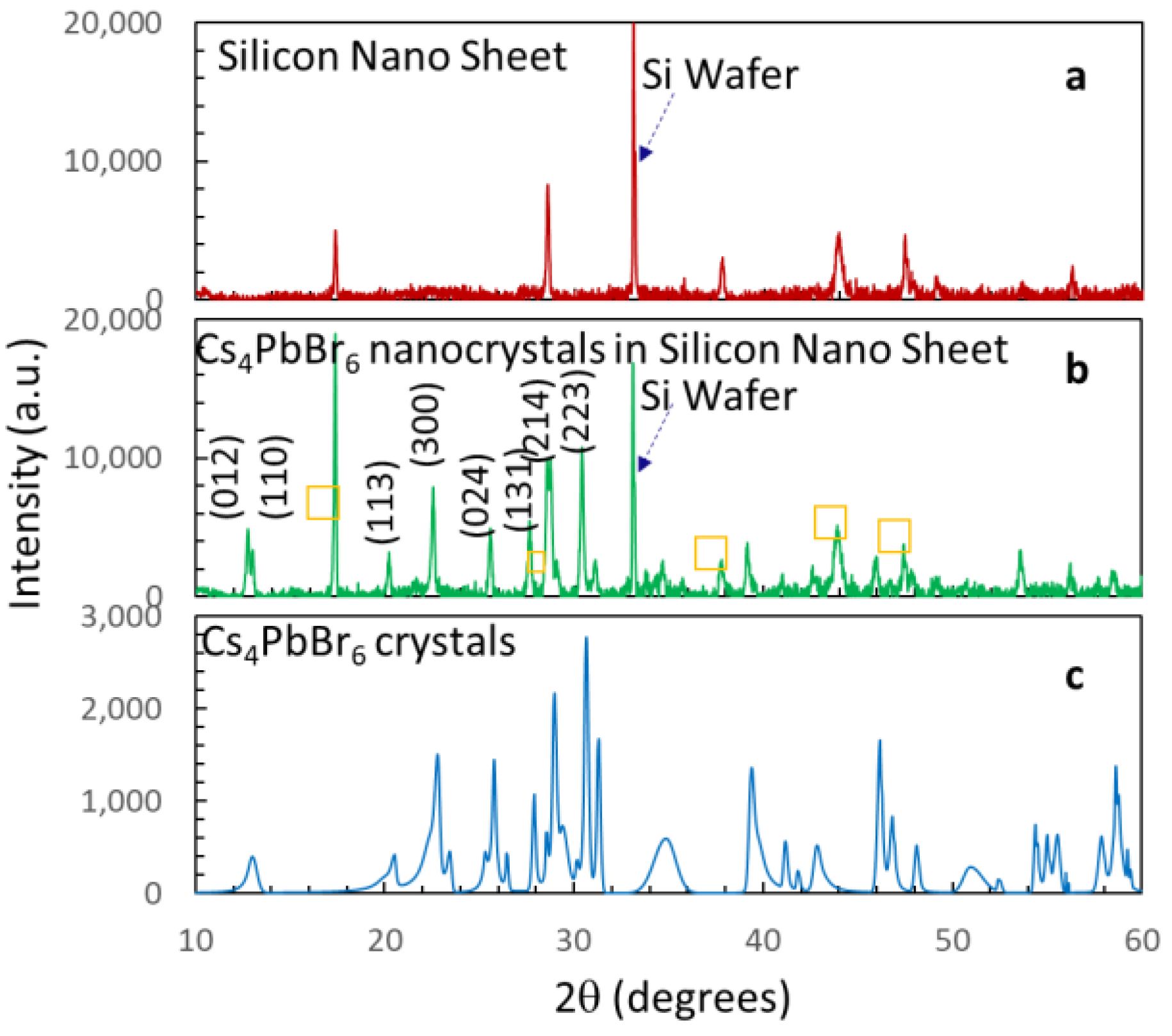
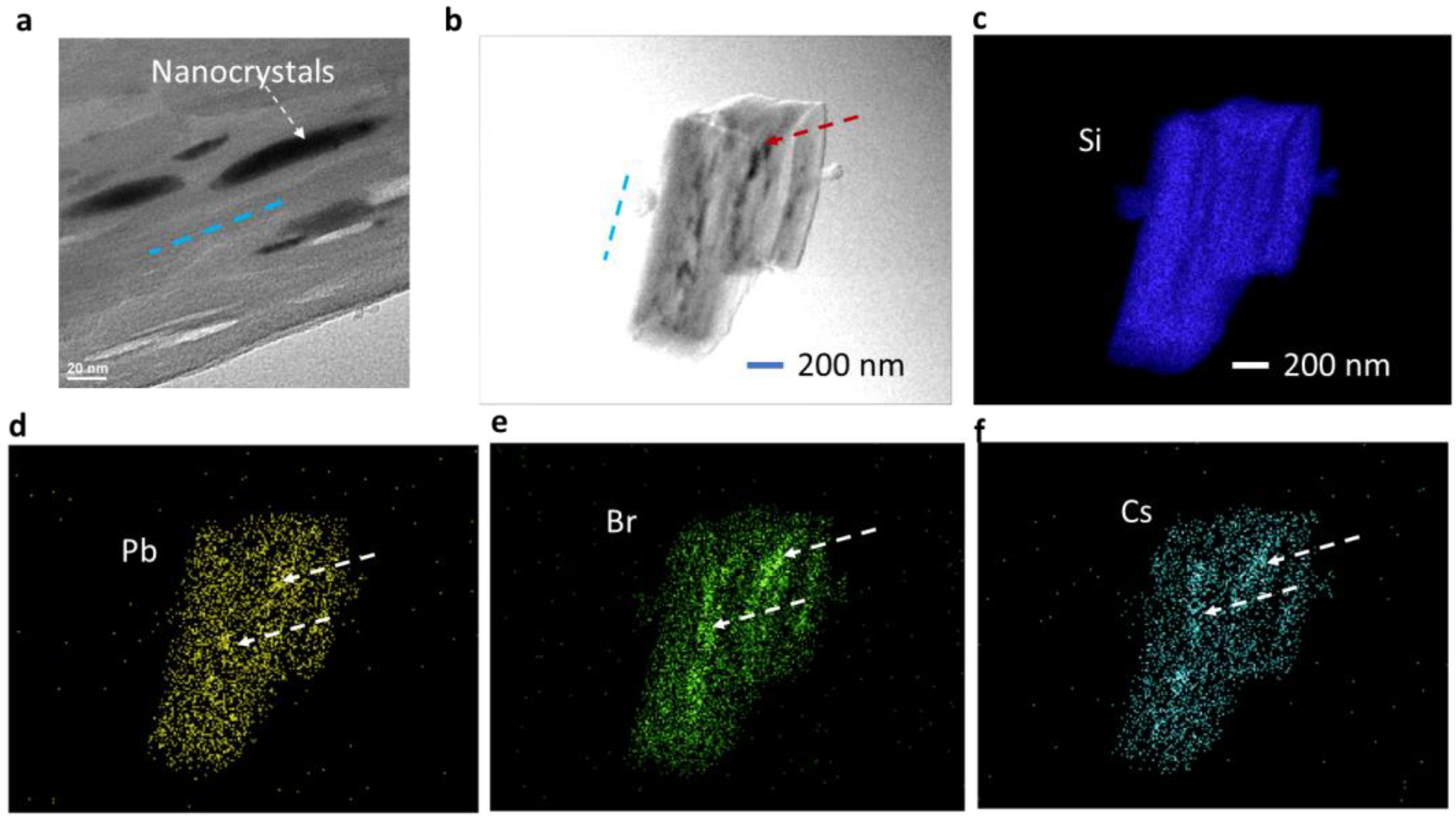
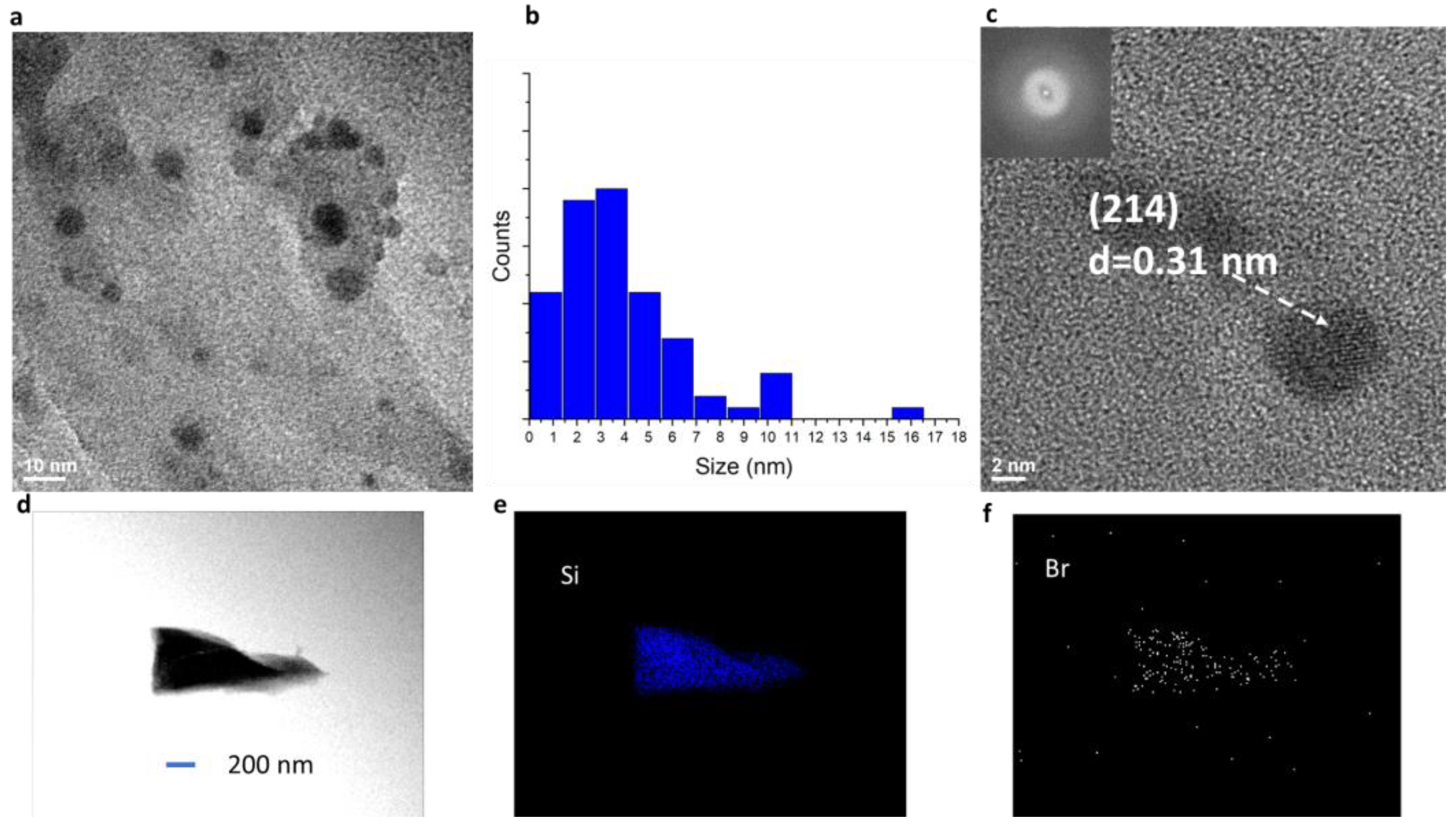
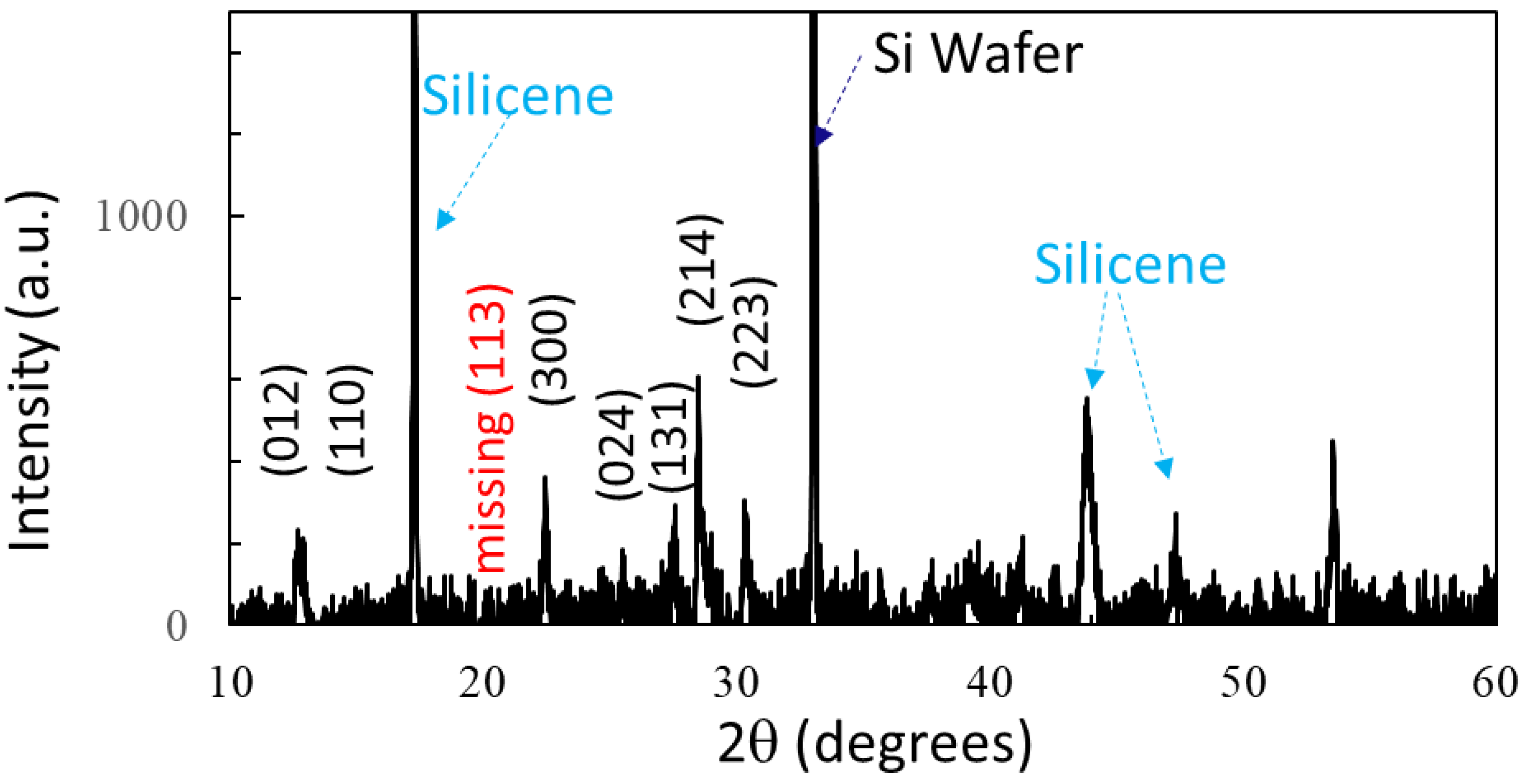
3.1. Material and Structural Characteristics

The prepared solutions of silicon nano-sheets and Cs4PbBr6 nanocrystals encapsulated in silicon nano-sheets were drop-casted onto a Si wafer and dried. Figure 1 shows the X-ray diffraction (XRD) of the silicon nano-sheet, the Cs4PbBr6 nanocrystals encapsulated in silicon nano-sheets, and the bulk Cs4PbBr6 crystals. The XRD peaks at 33.1° in Figure 1a,b belong to the Si wafer, as confirmed in the supporting information in reference [26]. Silicon nano-sheets have XRD peaks at 17.4°, 28.6°, 37.8°, 44.0°, 47.5°, 49.2°, and 56.5° (Figure 1a) [26]. These peaks appear in the XRD of Cs4PbBr6 nanocrystals (high concentration) encapsulated in silicon nano-sheets in Figure 1b, as labeled with yellow squares. The XRD peaks from Cs4PbBr6 nanocrystals in Figure 1b are located at 12.6°, 12.9°, 20.1°, 22.4°, 25.4°, 27.5°, 28.6°, and 30.3°, and are assigned to the low diffraction orders of the (012), (110), (113), (300), (024), (131), (214), and (223) planes, respectively. Figure 1c shows the XRD pattern of bulk Cs4PbBr6 for comparison. The XRD pattern in Figure 1c can be fitted to the hexagonal phase of Cs4PbBr6 with a = 13.73 Å, b = 13.73 Å, c = 13.73 Å, α = 90.0°, β = 90.0°, and γ = 120.0° (XRD database Card No.: 1538416). The XRD pattern of Cs4PbBr6 quantum dots encapsulated in silicon nano-sheets shows peaks from silicon nano-sheets only due to the low concentration. However, their presence is confirmed by TEM (vide infra).
Figure 2a shows a zoomed-in image (enlarged view) of a TEM image of Cs4PbBr6 ellipsoidal nanocrystals encapsulated in silicon nano-sheets. The dashed arrow in the figure indicates the location of one Cs4PbBr6 nanocrystal (dark region). All Cs4PbBr6 nanocrystals are elongated with the same orientation, as indicated by a dashed blue line, assuming they are in the same plane as a given silicon nano-sheet. From Figure 2a, we can observe that the nanocrystal size is not uniform; the elongated nanocrystals have a larger size in the middle than these at both sides of elongation. The stretching of the nanocrystals and different sizes along the long nanocrystals will be modeled for the explanation of the multiple peaks in the PL measurements.
Figure 2b shows a TEM image of one piece of sample for TEM-EDX study. The scale bars in2(b–f are the same. The dashed blue line indicates the nano-sheet orientation. One of the dark regions is indicated by an arrow. These nanocrystals in the dark regions are in the same orientation. Over 10 of them are revealed on the surface using TEM. Inside the bulk sample, TEM-EDX maps can reveal more information. The distribution of elements associated with the Cs4PbBr6 nanocrystals encapsulated in silicon nano-sheet perovskites (i.e., Si, Pb, Br, and Cs) is shown in Figure 2c–f, respectively. The elements of Si, Pb, Br, and Cs cover the whole piece of the sample in Figure 2b, as judged by the map shape. It is understandable that the map intensity of Si in Figure 2c is uniform due to the role of the host. The map intensity of Pb, Br, and Cs is not uniform. Especially in Figure 2e, it is very clear to see that the strong intensity regions (indicated by dashed white arrows, for example) correspond to the dark regions in Figure 2b.
The diffraction peaks from Cs4PbBr6 quantum dots did not show up in the XRD pattern due to their low concentration (diluted by 10 times). TEM allowed us to observe the quantum dots. Figure 3a shows a typical TEM image of Cs4PbBr6 pseudo-spherical quantum dots encapsulated in silicon nano-sheets. The size of the quantum dots is not uniform. Figure 3b shows the size distribution of the quantum dots in a range of 1 to 16 nm. The mean size is 4.67 nm. Figure 3c shows a high-resolution TEM (HRTEM) image of quantum dots and fast Fourier transform (FFT) patterns. A d-value of 0.31 nm was obtained, corresponding to the space between the (214) plane of hexagonal Cs4PbBr6. Figure 3d shows a TEM image of one piece of the sample and its distribution of elements associated with the Cs4PbBr6 quantum dots encapsulated in silicon nano-sheet perovskites in Figure 3e,f for Si and Br as an example, respectively. Si covers the whole sample in Figure 3e, while the map intensity of Br is not as dense as Si due to the low concentration of quantum dots.

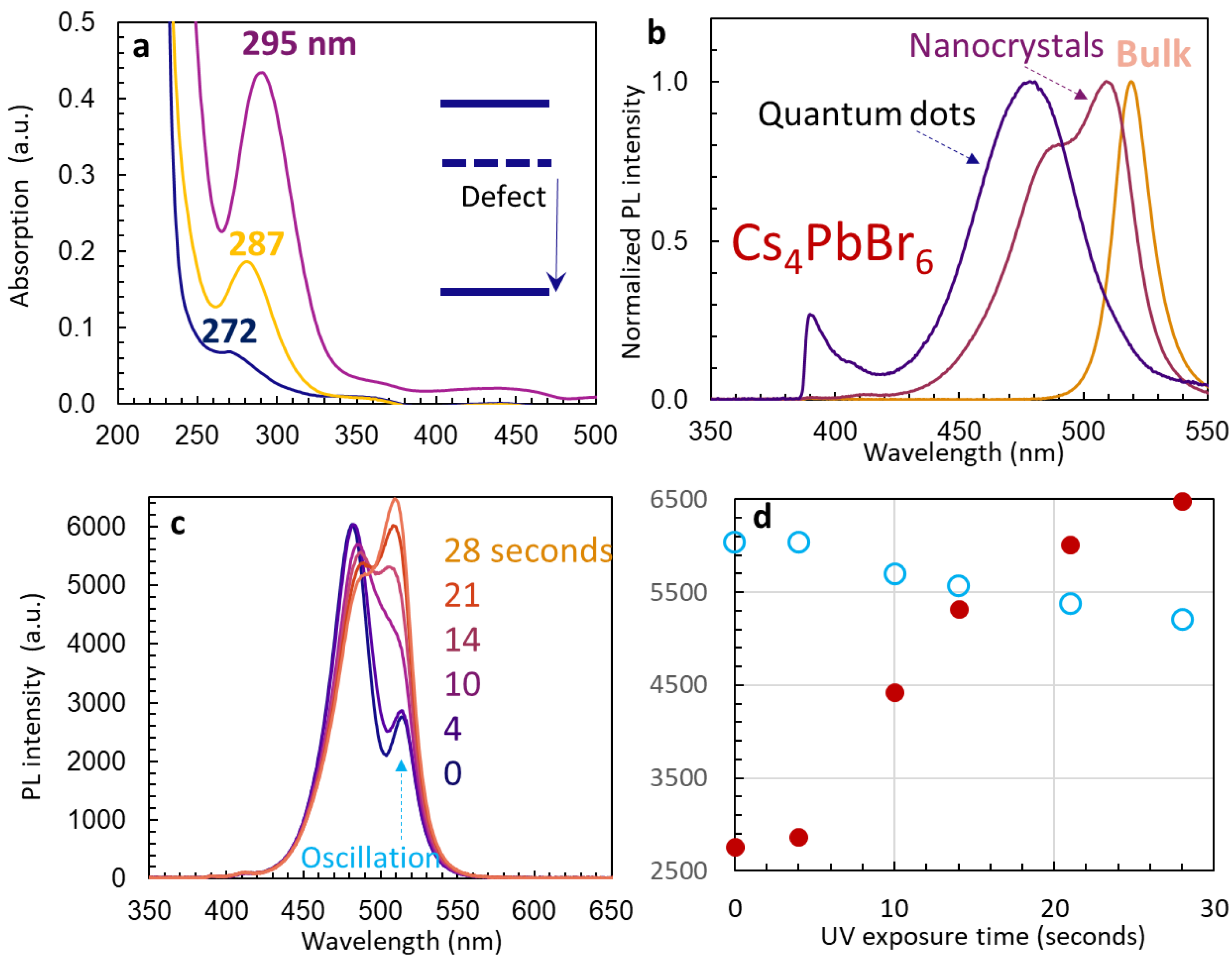
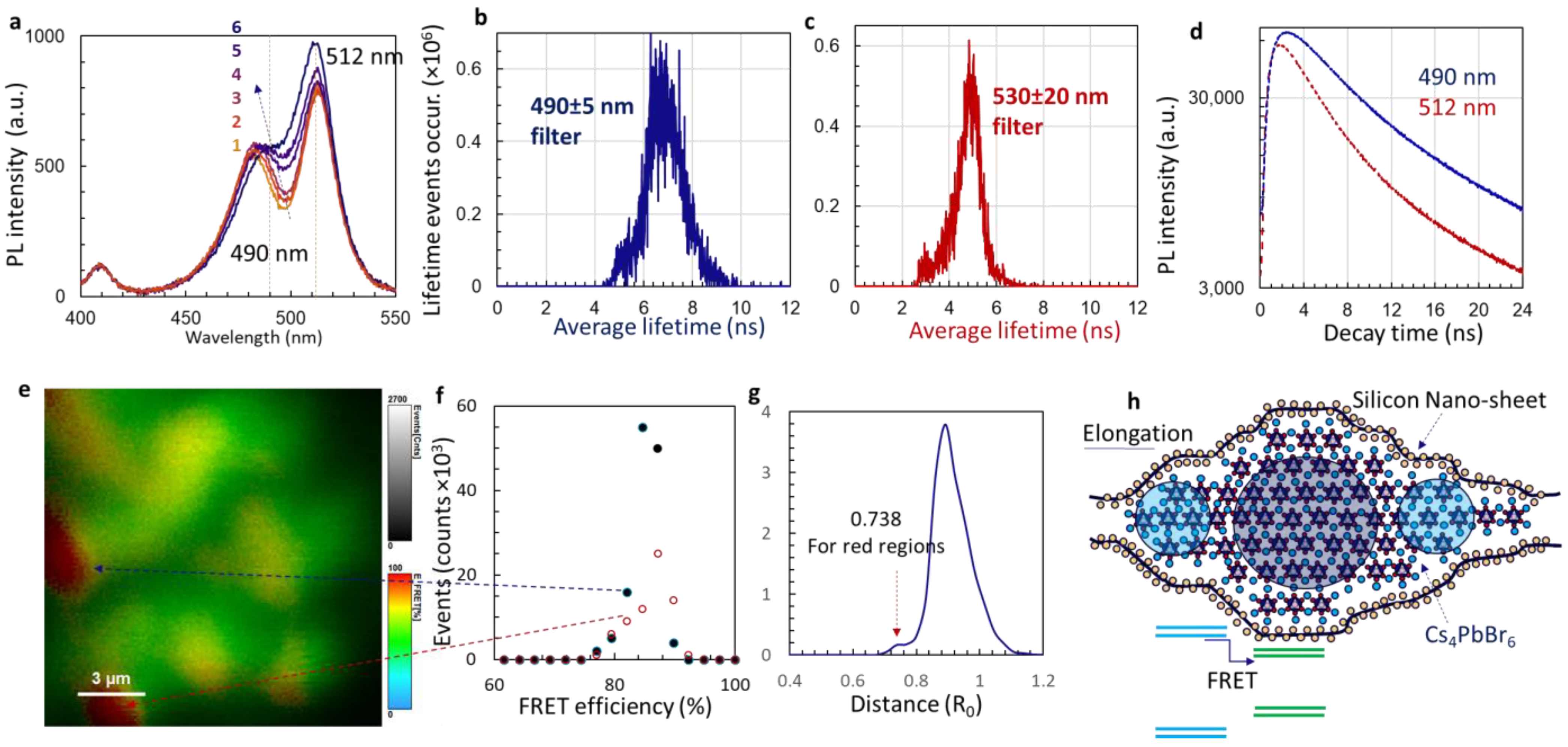
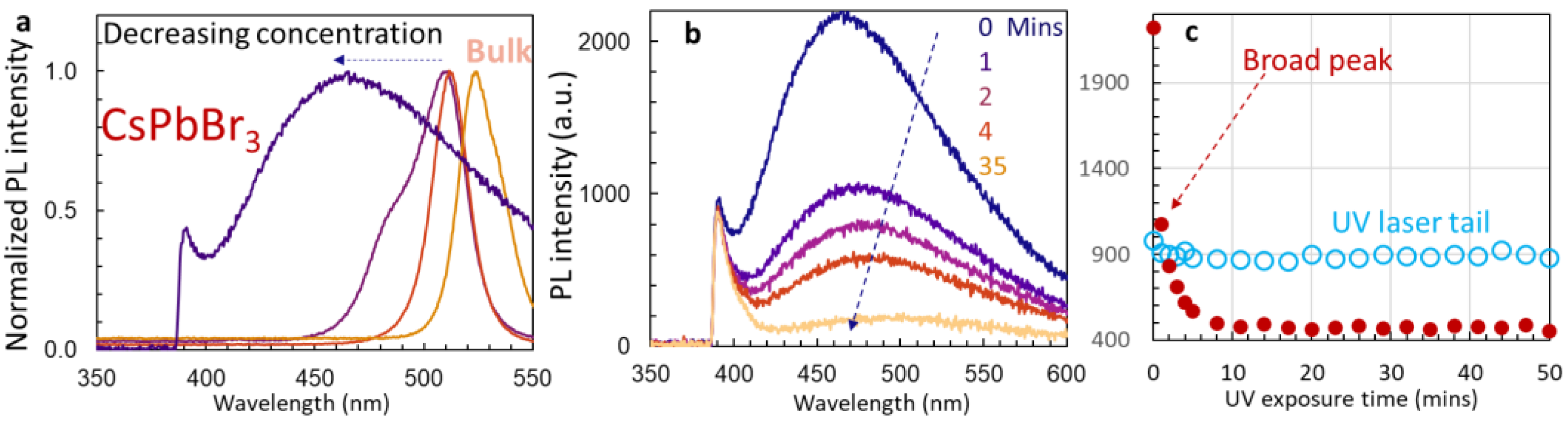
3.2. PL Spectra and Förster Resonance Energy Transfer

Firstly, we measured the absorption of bulk Cs4PbBr6 Cs4PbBr6 nanocrystals and quantum dots in DMSO solution before they were mixed with silicon nano-sheets, where narrow peaks were observed at 295, 287, and 272 nm, respectively. We then measured the PL for bulk Cs4PbBr6, its ellipsoidal nanocrystals, and pseudo-spherical quantum dots encapsulated in silicon nano-sheets. Figure 4b shows normalized PLs, with a peak position at 520 nm for bulk Cs4PbBr6, two peaks at 512 and 490 nm for Cs4PbBr6 nanocrystals, and a broad peak centered at 480 nm for Cs4PbBr6 quantum dots. With a small crystal size, the PL peak is blueshifted, similar to what has been observed in CsPbBr3 in silicene and bulk CsPbBr3. The broad peak of Cs4PbBr6 quantum dots in Figure 4b can be due to the un-passivated surfaces and its surface state. Similar to other results [29], Cs4PbBr6 had a very small spectral overlap of absorption and PL emission with a Stokes shift of up to 1.82 eV. Defect states due to Br-poor vacancy or local deformation of [PbBr6]4− octahedra were used to explain the large Stokes shift [29,30,31,32]. Although the shift of the narrow peak with the crystal size can be observed in Figure 4a, such a large Stokes shift poses a complexity in explaining the FRET below in Cs4PbBr6 in silicon nano-sheets.
The PL in Figure 4b for Cs4PbBr6 nanocrystals in silicon nano-sheets was measured after several minutes of UV exposure. In the short period of UV 375 nm laser exposure, the peak at 512 nm is very weak initially, then increases its intensity from 0 to 28 s, and finally its intensity is higher than the peak at 490 nm, as shown in Figure 4c. We also recorded a Video S1, “PL peak intensity oscillation”. We can see the increase in peak intensity at 512 nm, turning off the UV laser at 36–42 s, the dropping of the peak intensity, and its increase again after the UV laser is turned on. Figure 4d shows the peak intensity as a function of UV exposure time, where we see an increase in intensity by more than two times for 512 nm emission in 20 s.
In order to understand both the intensity oscillation of the 512 nm emission peak and the exchange of peak intensity of both PL lines in Cs4PbBr6 nanocrystals encapsulated in silicon nano-sheets, we measured the lifetime of PL peaks and FRET in the next steps. Due to the intensity change and shift of the PL peaks with UV laser exposure time, we measured the PL after the UV laser had been turned on for several minutes (typical time for PL lifetime imaging). We measured the PL for six times of the irradiation hardening, starting from yellow to dark blue as shown in Figure 5a. The irradiation-hardened Cs4PbBr6 nanocrystals had PL peaks at 490 and 512 nm. We used bandpass filters of 490 ± 5 nm (i.e., 485–495 nm) and 530 ± 20 nm (i.e., 510–550 nm) and measured the FLIM. After fitting and calculation, Figure 5b,c show the average lifetime histogram for the PL peaks at 490 and 512 nm, respectively. The lifetime events were controlled below 106 for measurement accuracy. As seen from Figure 5b,c, the average lifetime is centered at 6.8 ns for 490 nm and 5.0 ns for 512 nm. Their PL decay lines are shown in Figure 5d. As the nanocrystal size becomes smaller, the PL peak usually blueshifts [33]. The PL of 490 nm comes from a smaller nanocrystal than that of 512 nm. The more surface localized charges [34] (also the more surface trap states) in smaller nanocrystals, the higher the PL lifetime, which also makes the lifetime histogram curve broader in Figure 5b than that in Figure 5c.
Using bandpass filters of 490 ± 5 nm and 530 ± 20 nm, we measured the FLIM and calculated FRET events and efficiency between 490 nm and 512 nm as shown in Figure 5e. The FRET efficiency E [19] is defined in Equation (1):
E = 1 R R 0 6 + 1
where Ro is the distance between the Cs4PbBr6 donor (490 nm emission) and the Cs4PbBr6 acceptor (512 nm emission) with a FRET efficiency of 50%, and R is the distance between the donor and the acceptor. Non-uniformity in the FRET efficiency is clearly observed. Based on the scale bar, most of areas are covered by a green color with approximately 66% efficiency with a distance of 0.89 Ro, as also calculated by Equation (1). For the two red regions, we processed with the “region of interest” and obtained a FRET efficiency histogram in Figure 5f. Both red regions have a FRET efficiency of 86–87%, corresponding to a distance of 0.738 Ro, as indicated by the red arrow in Figure 5g, where the occurred FRET events over the map region are plotted with respect to R. Figure 5h shows a schematic of the proposed model of Cs4PbBr6 nanocrystals encapsulated in silicon nano-sheets with horizontal elongation, following the information that was obtained using TEM in Figure 2a,b for Cs4PbBr6 ellipsoidal nanocrystals in the dark regions. The circles in Figure 5h are for visual indication only. We have a schematic of wide (blue lines) and narrow (green lines) bandgaps for the Cs4PbBr6 nanocrystals above. FRET can occur between these wide and narrow bandgaps.

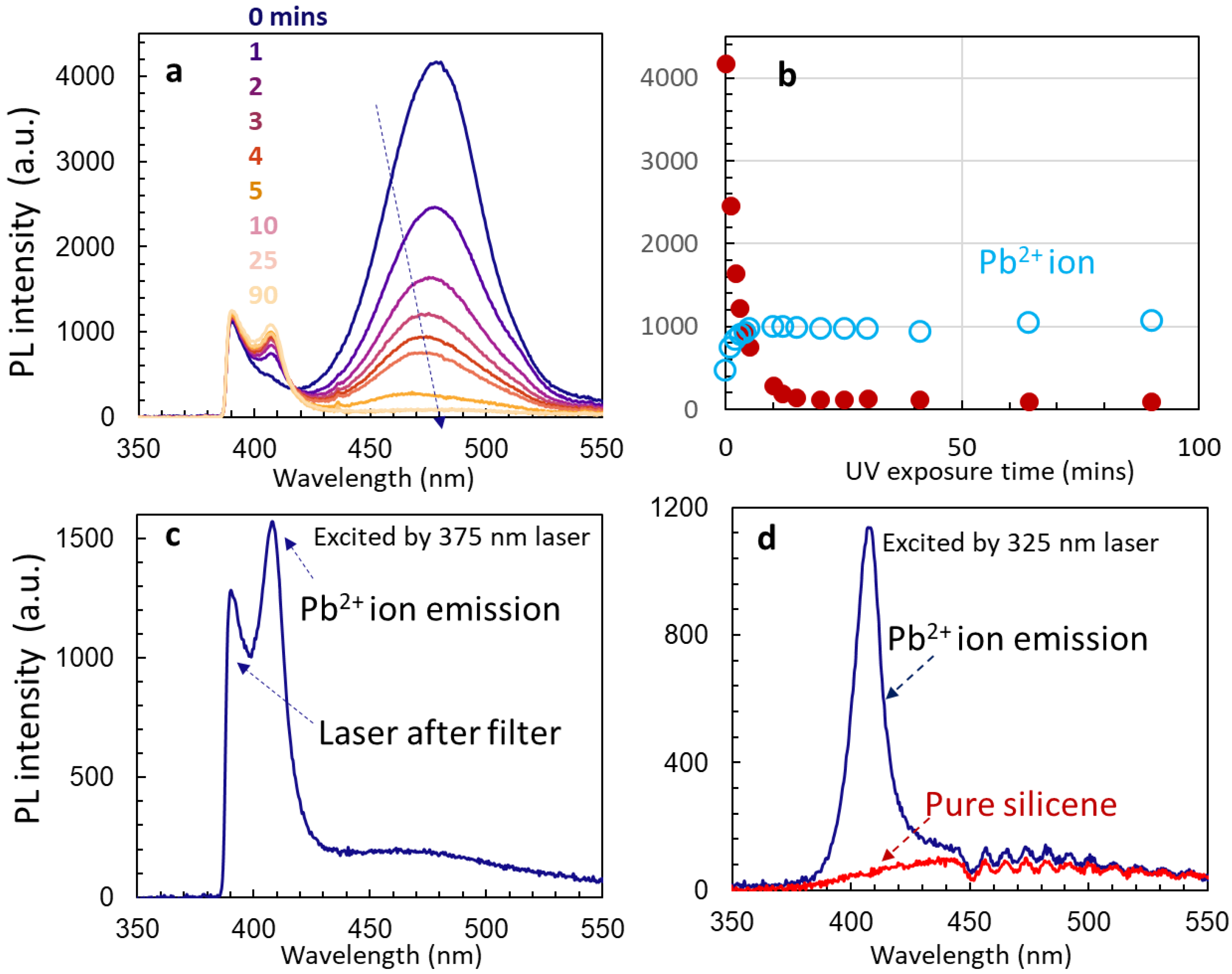
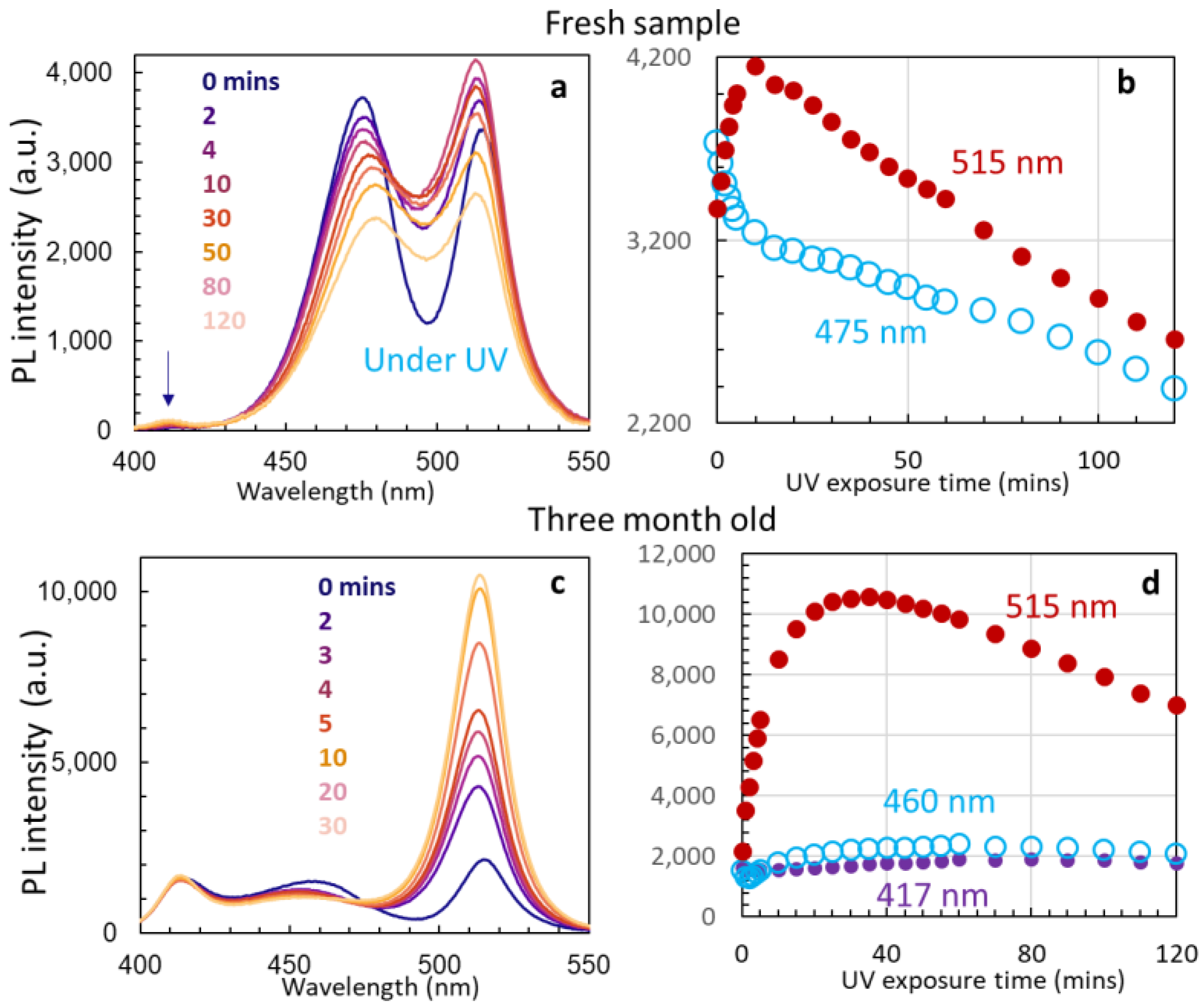
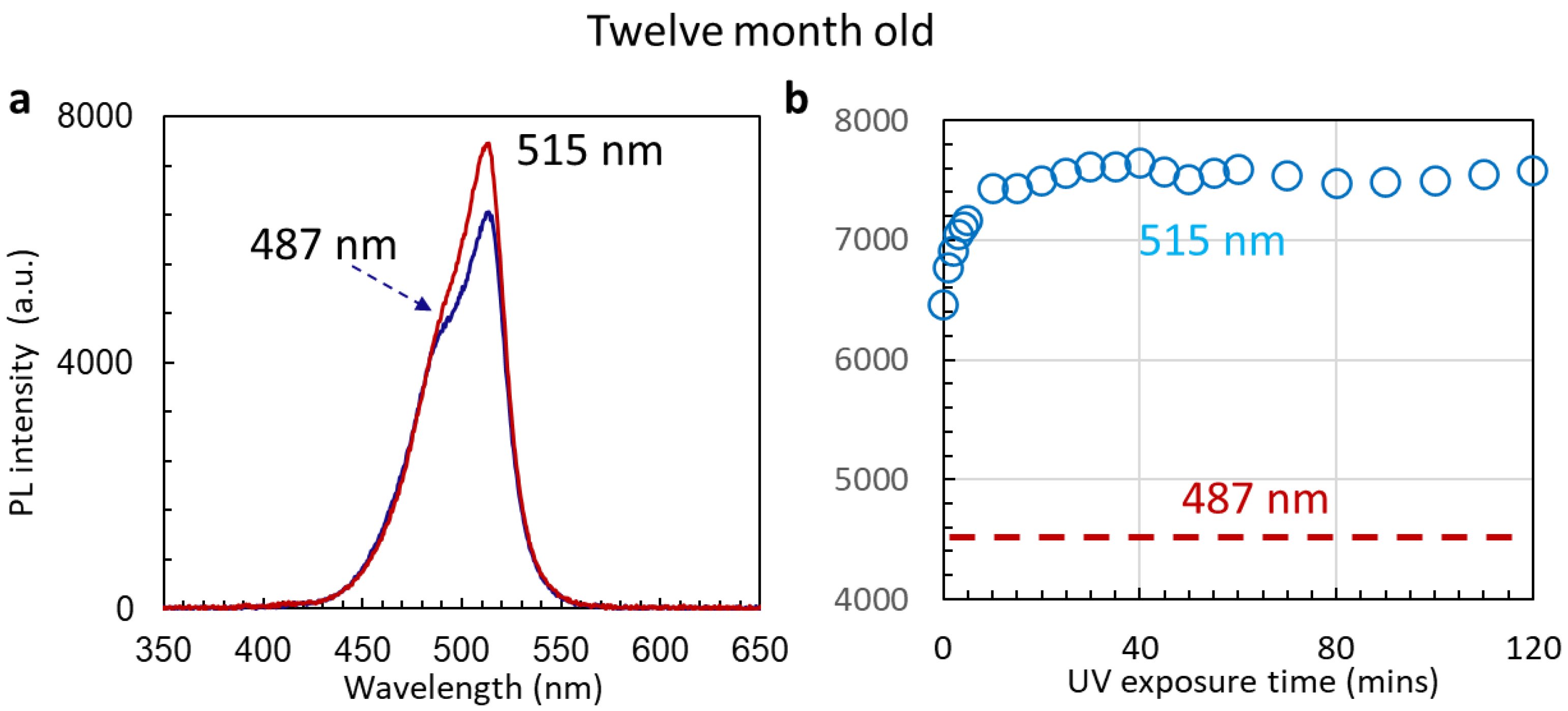
3.3. Stability of Un-Passivated Cs4PbBr6 and Enhanced PL Emissions

We present the stability of un-passivated Cs4PbBr6 quantum dots encapsulated in silicon nano-sheets, their non-uniformity, their Pb2+ ion emission, and their enhancement of 512 nm emission. Figure 6a shows the PL spectra of Cs4PbBr6 quantum dots encapsulated in silicon nano-sheets after continuous UV laser exposure for 0, 1, 2, 3, 4, 5, 10, 25, and 90 min. The broad peak centered at 483 nm drops in intensity very quickly within 5 s. The intensity of Pb2+ ion emission [31,32] at 410 nm increases quickly with increasing exposure. Figure 6b shows the PL intensities as a function of UV laser exposure time for these two peaks. At 12 min, the intensity of the 483 nm peaks reaches almost zero, while the Pb2+ ion emission reaches the maximum at 12 min and is stable up to the end of measurement (90 min), indicating that un-passivated Cs4PbBr6 quantum dots are not stable, and isolated Pb2+ ions are formed and are stable. After a longer UV exposure time, Pb2+ ion emission becomes stronger. Figure 6c shows the PL of Pb2+ ion emission after the UV degradation of Cs4PbBr6 quantum dots for 5 h. The peak below 400 nm is the emission tail of the 375 nm laser after a band cutoff filter. To confirm this, we excited the PL of degraded Cs4PbBr6 quantum dots using a UV 325 nm laser. Figure 6d shows the PL of the degraded Cs4PbBr6 quantum dots with one peak only, at 410 nm. We also show the PL spectrum of pure silicene, excited using a UV 325 nm laser for comparison. The silicene (silicon nano-sheets) has no PL between 350 and 550 nm.
We further studied the stability of Pb2+ ion emission. We picked up degraded Cs4PbBr6 quantum dots and monitored the intensity stability of the 410 nm peak (Pb2+ ion emission [31,32]) as shown in Figure 7a on day 1. The red circles in the figure indicate that the laser power is very stable. The intensity of Pb2+ ion emission changed slightly at the very beginning and then became stable. We measured the intensity of Pb2+ ion emission on days 3, 4, 10, and 22 for 2 h. Figure 7b plots the intensity of Pb2+ ion emission on day 22 as a representative example, and Figure 7c shows the intensity ratio of Pb2+ ion emission over the laser tail power. Overall, the intrinsic Pb2+ ion emission is stable.
With the above understanding of the stability of Pb2+ ions and the instability of Cs4PbBr6 quantum dots, we further studied a region of the sample where Cs4PbBr6 nanocrystals have three PL peaks at 515 nm, 475 nm, and 410 nm, as shown in Figure 8a. The shift of the 490 nm peak in Figure 5a to 475 nm in Figure 8a indicates smaller nanocrystal sizes in Figure 8a than that in Figure 5a. From Figure 8a,b, we can learn that the intensity of the PL peak of 515 nm is initially weaker than that of 475 nm, it increases at the very beginning of UV 375 nm exposure, it becomes stronger than that of 475 nm, and then it decreases in intensity with increasing exposure time. For the 475 nm peak, its intensity drops quickly at the very beginning of UV exposure and drops at a slower rate together with the 515 nm peak in Figure 8b. The dropping of intensity of both PL peaks can be caused by the instability of Cs4PbBr6 nanocrystals related to the 475 nm peak.
We waited for 3 months for the disappearance of the 475 nm peak. As shown in Figure 8c, the 3-month-old sample has a weak peak at 460 nm. However, the Pb2+ ion emission becomes relatively strong due to the degradation of Cs4PbBr6 nanocrystals. In such an aged sample, the intensity of PL 515 nm increases five times upon exposing the sample to a UV 375 nm laser for 15 min, and reaches the maximum after 30 min, as shown in Figure 8c,d. The Pb2+ ion emission at 417 nm was stable, and the intensity of 460 nm varied slightly. The stable PL of Pb2+ ion emission can lead to the possibility of photon recycling (the process of photon re-absorption and internal re-emission from Pb2+ to 515 nm) for the enhancement of 515 nm. Future research can be performed on the passivation of Cs4PbBr6 nanocrystals, then further encapsulated in silicon nano-sheets for photoelectric devices.
After 12 months of ambient storage of Cs4PbBr6 nanocrystals in silicon nano-sheets, we were still able to observe the FRET, as shown in Figure 9. This time, the peak intensity at 487 nm was stable during the measurement period from 0 to 120 min. The peak intensity at 515 nm was stronger than the 487 nm peak. Its intensity increased from 6400 to 7600 in a short time, then stayed almost constant. By the comparison of two peak intensities in Figure 9a,b, we can see that FRET plays a crucial role in the PL enhancement of 515 nm for PeLED application.

4. Discussion

Cs4PbBr6 was reported to be stable under alpha-particle excitation [35]. We first discussed the UV irradiation effect on Cs4PbBr6 nanocrystals encapsulated in silicon nano-sheets. After 12 months, we rechecked XRD for the sample as shown in Figure 10. As we can see from the figure, XRD peaks from silicon nano-sheet were still observed, indicating silicon nano-sheets were stable for 12 months. We can still observe the XRD peaks from Cs4PbBr6 nanocrystals at 12.6°, 12.9°, 22.4°, 25.4°, 27.5°, 28.6°, and 30.3° due to the low diffraction orders of the (012), (110), (300), (024), (131), (214), and (223) planes, respectively. Diffraction from the (113) plane is missing and XRD peaks are weaker from the aged sample than the fresh one, corresponding to the fact that the broad peak around 460 nm from the Cs4PbBr6 became weak and Pb2+ emission appeared after UV irradiation in Figure 6 and Figure 8.
We further discussed why the PL peak from Cs4PbBr6 quantum dots is broader than those from nanocrystal or bulk material. Usually, the PL peak becomes narrower when the nanocrystal size becomes smaller due to the quantum discrete state [33]. We assume that there are many surface trap states in the interface of silicon nano-sheets and un-passivated quantum dots, leading to a broad PL peak. To confirm this assumption, we compared our results for Cs4PbBr6 with those for CsPbBr3. We prepared CsPbBr3 encapsulated in silicon nano-sheets with decreasing concentrations (the quantity of the concentration was ignored) and measured their PL as shown in Figure 11a. Similarly, a broad peak was observed at the low concentration of CsPbBr3 in silicon nano-sheets. The intensity of the broad peak dropped quickly during the UV 375 nm laser irradiation, as shown in Figure 11b,c. The only difference between the Cs4PbBr6 and CsPbBr3 samples is that there is no Pb2+ ion emission in the CsPbBr3 sample.

5. Conclusions

Silicon nano-sheets have been used to encapsulate Cs4PbBr6 nanocrystals for their potential integration with traditional semiconductors. For low concentrations of un-passivated Cs4PbBr6 in silicon nano-sheets, pseudo-spherical quantum dots were formed with a broad PL peak, which was not stable upon irradiation with a UV 375 nm laser. The Pb2+ ion emission was stable upon the degradation of Cs4PbBr6 quantum dots. For high concentrations of un-passivated Cs4PbBr6 in silicon nano-sheets, ellipsoidal nanocrystals were observed. The intensity oscillation of two PL peaks was observed upon the UV laser being switched on and off after exposure, and explained by FRET with an efficiency of up to 86–87%. In a sample with three PL peaks at 515, 475, and 410 nm, the degraded (aged for 3 months) sample showed stable Pb2+ ion/silicene emission and enhanced intensity by five times for 515 nm, presumably due to photon recycling from Pb2+ ion/silicene emission to 515 nm.

Supplementary Materials

The following supporting information can be downloaded at https://www.mdpi.com/article/10.3390/nano14191596/s1, Video S1: PL peak intensity oscillation.

Author Contributions

Conceptualization, Y.L., J.C. and R.G.R.; methodology, R.G.R., Y.L., A.H.M. and J.C.; software, N.H., A.H.M. and S.V.; formal analysis, A.H.M., R.G.R. and Y.L.; investigation, A.H.M., R.G.R., N.H., B.S. and S.V.; resources, J.L.C., B.S., J.C. and Y.L.; Material synthesis, B.D., M.C., Q.J. and R.G.R.; writing—original draft preparation, A.H.M., R.G.R., Q.J. and Y.L.; writing—review and editing, all; visualization, Y.L. and Y.J.; supervision, Q.J., A.B.K., M.M., J.L.C., J.C. and Y.L.; funding acquisition, Q.J., A.B.K., M.M., J.C. and Y.L. All authors have read and agreed to the published version of the manuscript.

Funding

This research was partially supported by the U.S. National Science Foundation, grant number 2128367, grant number 2228891 and by the Department of Energy/National Nuclear Security Administration under Award Number DE-NA0004114.

Data Availability Statement

The data will be available upon request.

Conflicts of Interest

The authors declare no conflicts of interest. This report was prepared as an account of work sponsored by an agency of the United States Government. Neither the United States Government nor any agency thereof, nor any of their employees, makes any warranty, express or implied, or assumes any legal liability or responsibility for the accuracy, completeness, or usefulness of any information, apparatus, product, or process disclosed, or represents that its use would not infringe privately owned rights. Reference herein to any specific commercial product, process, or service by trade name, trademark, manufacturer, or otherwise does not necessarily constitute or imply its endorsement, recommendation, or favoring by the United States Government or any agency thereof. The views and opinions of the authors expressed herein do not necessarily state or reflect those of the United States Government or any agency thereof.

References

  1. Xing, G.; Mathews, N.; Lim, S.S.; Yantara, N.; Liu, X.; Sabba, D.; Grätzel, M.; Mhaisalkar, S.; Sum, T.C. Low-Temperature Solution-Processed Wavelength-Tunable Perovskites for Lasing. Nat. Mater. 2014, 13, 476–480. [Google Scholar] [CrossRef] [PubMed]
  2. Tan, H.; Jain, A.; Voznyy, O.; Lan, X.; García de Arquer, F.P.; Fan, J.Z.; Quintero-Bermudez, R.; Yuan, M.; Zhang, B.; Zhao, Y.; et al. Efficient and Stable Solution-Processed Planar Perovskite Solar Cells via Contact Passivation. Science 2017, 355, 722–726. [Google Scholar] [CrossRef] [PubMed]
  3. Nie, W.; Tsai, H.; Asadpour, R.; Blancon, J.-C.; Neukirch, A.J.; Gupta, G.; Crochet, J.J.; Chhowalla, M.; Tretiak, S.; Alam, M.A.; et al. High-Efficiency Solution-Processed Perovskite Solar Cells with Millimeter-Scale Grains. Science 2015, 347, 522–525. [Google Scholar] [CrossRef] [PubMed]
  4. Zhang, L.; Hu, S.; Guo, M.; Ren, Y.; Wei, L.; Li, W.; Lin, F.; Yang, Z.; Yang, Z.; Liu, C.; et al. Manipulation of Charge Dynamics for Efficient and Bright Blue Perovskite Light-Emitting Diodes with Chiral Ligands. Adv. Mater. 2023, 35, 2302059. [Google Scholar] [CrossRef]
  5. Finkenauer, B.P.; Akriti; Ma, K.; Dou, L. Degradation and Self-Healing in Perovskite Solar Cells. ACS Appl. Mater. Interfaces 2022, 14, 24073–24088. [Google Scholar] [CrossRef]
  6. Jiao, H.; Ni, Z.; Shi, Z.; Fei, C.; Liu, Y.; Dai, X.; Huang, J. Perovskite Grain Wrapping by Converting Interfaces and Grain Boundaries into Robust and Water-Insoluble Low-Dimensional Perovskites. Sci. Adv. 2022, 8, abq4524. [Google Scholar] [CrossRef]
  7. Chen, S.; Dai, X.; Xu, S.; Jiao, H.; Zhao, L.; Huang, J. Stabilizing Perovskite-Substrate Interfaces for High-Performance Perovskite Modules. Science 2021, 373, 902–907. [Google Scholar] [CrossRef]
  8. Gonzalez-Rodriguez, R.; Hathaway, E.; Lin, Y.; Coffer, J.L.; Cui, J. Encapsulated MAPbBr3 in Nickel Oxide Nanotubes and Their Electroluminescence. Nanoscale 2022, 14, 6417–6424. [Google Scholar] [CrossRef]
  9. Abdi-Jalebi, M.; Andaji-Garmaroudi, Z.; Cacovich, S.; Stavrakas, C.; Philippe, B.; Richter, J.M.; Alsari, M.; Booker, E.P.; Hutter, E.M.; Pearson, A.J.; et al. Maximizing and Stabilizing Luminescence from Halide Perovskites with Potassium Passivation. Nature 2018, 555, 497–501. [Google Scholar] [CrossRef]
  10. Xiong, S.; Hou, Z.; Zou, S.; Lu, X.; Yang, J.; Hao, T.; Zhou, Z.; Xu, J.; Zeng, Y.; Xiao, W.; et al. Direct Observation on P- to n-Type Transformation of Perovskite Surface Region during Defect Passivation Driving High Photovoltaic Efficiency. Joule 2021, 5, 467–480. [Google Scholar] [CrossRef]
  11. Fang, H.-H.; Yang, J.; Tao, S.; Adjokatse, S.; Kamminga, M.E.; Ye, J.; Blake, G.R.; Even, J.; Loi, M.A. Unravelling Light-Induced Degradation of Layered Perovskite Crystals and Design of Efficient Encapsulation for Improved Photostability. Adv. Funct. Mater. 2018, 28, 1800305. [Google Scholar] [CrossRef]
  12. Raja, S.N.; Bekenstein, Y.; Koc, M.A.; Fischer, S.; Zhang, D.; Lin, L.; Ritchie, R.O.; Yang, P.; Alivisatos, A.P. Encapsulation of Perovskite Nanocrystals into Macroscale Polymer Matrices: Enhanced Stability and Polarization. ACS Appl. Mater. Interfaces 2016, 8, 35523–35533. [Google Scholar] [CrossRef] [PubMed]
  13. Konidakis, I.; Karagiannaki, A.; Stratakis, E. Advanced Composite Glasses with Metallic, Perovskite, and Two-Dimensional Nanocrystals for Optoelectronic and Photonic Applications. Nanoscale 2022, 14, 2966–2989. [Google Scholar] [CrossRef] [PubMed]
  14. He, H.; Cui, Y.; Li, B.; Wang, B.; Jin, C.; Yu, J.; Yao, L.; Yang, Y.; Chen, B.; Qian, G. Confinement of Perovskite-QDs within a Single MOF Crystal for Significantly Enhanced Multiphoton Excited Luminescence. Adv. Mater. 2019, 31, 1806897. [Google Scholar] [CrossRef] [PubMed]
  15. Lin, Y.; Fan, X.; Yang, X.; Zheng, X.; Huang, W.; Shangguan, Z.; Wang, Y.; Kuo, H.; Wu, T.; Chen, Z. Remarkable Black-Phase Robustness of CsPbI3 Nanocrystals Sealed in Solid SiO2/AlOx Sub-Micron Particles. Small 2021, 17, 2103510. [Google Scholar] [CrossRef]
  16. Park, S.M.; Wei, M.; Xu, J.; Atapattu, H.R.; Eickemeyer, F.T.; Darabi, K.; Grater, L.; Yang, Y.; Liu, C.; Teale, S.; et al. Engineering Ligand Reactivity Enables High-Temperature Operation of Stable Perovskite Solar Cells. Science 2023, 381, 209–215. [Google Scholar] [CrossRef]
  17. Fan, X.; Wang, S.; Yang, X.; Zhong, C.; Chen, G.; Yu, C.; Chen, Y.; Wu, T.; Kuo, H.; Lin, Y.; et al. Brightened Bicomponent Perovskite Nanocomposite Based on Förster Resonance Energy Transfer for Micro-LED Displays. Adv. Mater. 2023, 35, 2300834. [Google Scholar] [CrossRef]
  18. Rabouw, F.T.; den Hartog, S.A.; Senden, T.; Meijerink, A. Photonic Effects on the Förster Resonance Energy Transfer Efficiency. Nat. Commun. 2014, 5, 3610. [Google Scholar] [CrossRef]
  19. Zhang, B.; Lyu, G.; Kelly, E.A.; Evans, R.C. Förster Resonance Energy Transfer in Luminescent Solar Concentrators. Adv. Sci. 2022, 9, 2201160. [Google Scholar] [CrossRef]
  20. Mishra, L.; Behera, R.K.; Panigrahi, A.; Sarangi, M.K. Förster Resonance Energy Transfer Assisted Enhancement in Optoelectronic Properties of Metal Halide Perovskite Nanocrystals. J. Phys. Chem. Lett. 2022, 13, 4357–4364. [Google Scholar] [CrossRef]
  21. Song, Y.; Zhang, C.; Liu, W.; Li, X.; Long, H.; Wang, K.; Wang, B.; Lu, P. High-Efficiency Energy Transfer in Perovskite Heterostructures. Opt. Express 2018, 26, 18448. [Google Scholar] [CrossRef] [PubMed]
  22. Panuganti, S.; Besteiro, L.V.; Vasileiadou, E.S.; Hoffman, J.M.; Govorov, A.O.; Gray, S.K.; Kanatzidis, M.G.; Schaller, R.D. Distance Dependence of Förster Resonance Energy Transfer Rates in 2D Perovskite Quantum Wells via Control of Organic Spacer Length. J. Am. Chem. Soc. 2021, 143, 4244–4252. [Google Scholar] [CrossRef] [PubMed]
  23. Li, S.; Liu, G.; Liu, Q.; Nie, L.; Yao, G.; Zeng, F.; He, Y.; Xiang, W. Ultrastable Zero-Dimensional Cs4PbBr6 Perovskite Quantum Dot Glass. ACS Sustain. Chem. Eng. 2020, 8, 10646–10652. [Google Scholar] [CrossRef]
  24. Kim, H.; Park, J.H.; Kim, K.; Lee, D.; Song, M.H.; Park, J. Highly Emissive Blue Quantum Dots with Superior Thermal Stability via In Situ Surface Reconstruction of Mixed CsPbBr3–Cs4PbBr6 Nanocrystals. Adv. Sci. 2022, 9, 2104660. [Google Scholar] [CrossRef] [PubMed]
  25. Leitão, M.F.; Islim, M.S.; Yin, L.; Viola, S.; Watson, S.; Kelly, A.; Dong, Y.; Li, X.; Zeng, H.; Videv, S.; et al. Pump-Power-Dependence of a CsPbBr3-in-Cs4PbBr6 Quantum Dot Color Converter. Opt. Mater. Express 2019, 9, 3504. [Google Scholar] [CrossRef]
  26. Gonzalez-Rodriguez, R.; Hathaway, E.; Paulette, H.; Coffer, J.L.; Lin, Y.; Cui, J. Two-Dimensional Quantum-Confined CsPbBr3 in Silicene for LED Applications. ACS Appl. Nano Mater. 2023, 6, 4028–4033. [Google Scholar] [CrossRef]
  27. Saidaminov, M.I.; Almutlaq, J.; Sarmah, S.; Dursun, I.; Zhumekenov, A.A.; Begum, R.; Pan, J.; Cho, N.; Mohammed, O.F.; Bakr, O.M. Pure Cs4PbBr6: Highly Luminescent Zero-Dimensional Perovskite Solids. ACS Energy Lett. 2016, 1, 840–845. [Google Scholar] [CrossRef]
  28. Gonzalez-Rodriguez, R.; del Castillo, R.M.; Hathaway, E.; Lin, Y.; Coffer, J.L.; Cui, J. Silicene/Silicene Oxide Nanosheets for Broadband Photodetectors. ACS Appl. Nano Mater. 2022, 5, 4325–4335. [Google Scholar] [CrossRef]
  29. Zhao, H.; Sun, R.; Wang, Z.; Fu, K.; Hu, X.; Zhang, Y. Zero-Dimensional Perovskite Nanocrystals for Efficient Luminescent Solar Concentrators. Adv. Funct. Mater. 2019, 29, 1902262. [Google Scholar] [CrossRef]
  30. Benin, B.M.; Dirin, D.N.; Morad, V.; Wörle, M.; Yakunin, S.; Rainò, G.; Nazarenko, O.; Fischer, M.; Infante, I.; Kovalenko, M.V. Highly Emissive Self-Trapped Excitons in Fully Inorganic Zero-Dimensional Tin Halides. Angew. Chem. Int. Ed. 2018, 57, 11329–11333. [Google Scholar] [CrossRef]
  31. Yin, J.; Zhang, Y.; Bruno, A.; Soci, C.; Bakr, O.M.; Brédas, J.-L.; Mohammed, O.F. Intrinsic Lead Ion Emissions in Zero-Dimensional Cs4PbBr6 Nanocrystals. ACS Energy Lett. 2017, 2, 2805–2811. [Google Scholar] [CrossRef]
  32. Almutlaq, J.; Yin, J.; Mohammed, O.F.; Bakr, O.M. The Benefit and Challenges of Zero-Dimensional Perovskites. J. Phys. Chem. Lett. 2018, 9, 4131–4138. [Google Scholar] [CrossRef] [PubMed]
  33. Wen, X.; Zhang, P.; Smith, T.A.; Anthony, R.J.; Kortshagen, U.R.; Yu, P.; Feng, Y.; Shrestha, S.; Coniber, G.; Huang, S. Tunability Limit of Photoluminescence in Colloidal Silicon Nanocrystals. Sci. Rep. 2015, 5, 12469. [Google Scholar] [CrossRef] [PubMed]
  34. Chen, X.; Lin, X.; Zhou, L.; Sun, X.; Li, R.; Chen, M.; Yang, Y.; Hou, W.; Wu, L.; Cao, W.; et al. Blue Light-Emitting Diodes Based on Colloidal Quantum Dots with Reduced Surface-Bulk Coupling. Nat. Commun. 2023, 14, 284. [Google Scholar] [CrossRef]
  35. Li, Y.; Shao, W.; Chen, L.; Wang, J.; Nie, J.; Zhang, H.; Zhang, S.; Gao, R.; Ouyang, X.; Ouyang, X.; et al. Lead-Halide Cs4PbBr6 Single Crystals for High-Sensitivity Radiation Detection. NPG Asia Mater. 2021, 13, 40. [Google Scholar] [CrossRef]
Figure 1. XRD patterns of silicon nano-sheets on Si wafer (a), Cs4PbBr6 nanocrystals encapsulated in silicon nano-sheets (b), and bulk Cs4PbBr6 (c). XRD peaks from Si wafer substrate are labeled with dashed arrows. XRD peaks from silicon nano-sheets are labeled with squares in (b).
Nanomaterials 14 01596 g001
Figure 2. (a) Zoomed-in TEM image of Cs4PbBr6 nanocrystals encapsulated in silicon nano-sheets; (b) TEM image of one piece of sample of Cs4PbBr6 nanocrystals encapsulated in silicon nano-sheets for TEM-EDX. TEM-EDX map of Si (c), Pb (d), Br (e), and Cs (f). Cs4PbBr6 nanocrystals are pointed out by dashed arrows in (a,b). Same scale bar is used for (bf). White arrows in (df) are for region with strong intensity. Dashed lines in (a,b) indicate nano-sheet orientation.
Nanomaterials 14 01596 g002
Figure 3. (a) TEM image of Cs4PbBr6 quantum dots encapsulated in silicon nano-sheets; (b) size distribution of Cs4PbBr6 quantum dots encapsulated in silicon nano-sheets. (c) High resolution TEM (HRTEM) image of Cs4PbBr6 quantum dots and corresponding FFT. TEM of one piece of sample (d) and its TEM-EDX map of Si (e) and Br (f). Same scale bar is used for (df).
Nanomaterials 14 01596 g003
Figure 4. (a) Absorption of bulk Cs4PbBr6 (pink line), Cs4PbBr6 nanocrystals (yellow line), and quantum dots (blue line) in DMSO solution. (b) Normalized PL spectra of bulk Cs4PbBr6 (yellow line), Cs4PbBr6 nanocrystals (pink line), and quantum dots (blue line) encapsulated in silicon nano-sheets. (c) PL spectra of Cs4PbBr6 nanocrystals encapsulated in silicon nano-sheets at 0, 4, 10, 14, 21, and 28 s after UV excitation laser is turned on. (d) PL intensity at two wavelengths (512 nm in red and 490 nm in blue) as a function of UV exposure time.
Nanomaterials 14 01596 g004
Figure 5. (a) PL spectra measured after Cs4PbBr6 nanocrystals encapsulated in silicon nano-sheets were exposed to UV 375 nm laser for several minutes. Six of them were measured starting with “1” and ending with “6”. (b,c) Average PL lifetime histogram measured with bandpass filters of 490 ± 5 nm (i.e., 485–495 nm) (b) and 530 ± 20 nm (c). (d) PL intensity decay curves for 490 and 512 nm. (e) Intensity and efficiency of FRET and (f) FRET efficiency histogram for two red regions in (d) as indicated by dashed arrows. (g) Occurred FRET events at different distances. (h) Schematic of elongated Cs4PbBr6 nanocrystals encapsulated in silicon nano-sheets. Circles show different crystal sizes. Different sizes lead to different bandgaps for FRET.
Nanomaterials 14 01596 g005
Figure 6. (a) PL spectra of Cs4PbBr6 quantum dots encapsulated in silicon nano-sheets after different lengths of UV laser exposure of 0, 1, 2, 3, 4, 5, 10, 25, and 90 min; (b) PL intensities as a function of UV laser exposure time for 483 nm (red circles) and Pb2+ ion emission at 410 nm; (c) PL of Pb2+ ion emission after UV degradation of Cs4PbBr6 quantum dots for 5 h. (d) PL of degraded Cs4PbBr6 quantum dots and pure silicene, excited using UV 325 nm laser.
Nanomaterials 14 01596 g006
Figure 7. The PL intensity of Pb2+ ion emission and laser tail intensity after a filter on day 1 (a) and day 22 (b). (c) The laser intensity is stable and is used as a reference for the intensity ratio of Pb2+ ion emission on different days.
Nanomaterials 14 01596 g007
Figure 8. (a) PL spectra in a region of the sample where Cs4PbBr6 nanocrystals have three PL peaks at 515 nm, 475 nm, and the weak 410 nm line (as indicated by an arrow) after 0, 2, 4, 10, 30, 50 80, and 120 min of UV 375 nm laser exposure; (b) PL intensities of 515 nm and 475 nm as a function of length of UV 375 nm laser exposure. (c) PL spectra from 3-month-old sample after 0, 2, 3, 4, 5, 10, 20, and 30 min of UV 375 nm laser exposure; (d) PL intensities of 515 nm, 460 nm, and 417 nm as a function of length of UV 375 nm laser exposure.
Nanomaterials 14 01596 g008
Figure 9. (a) PL spectra of 12-month-old sample of Cs4PbBr6 nanocrystals encapsulated in silicon nano-sheets at 0 (blue line) and 120 min (red line) after UV excitation laser is turned on. (b) PL intensity at 515 nm as function of UV exposure time. We did not conduct peak intensity fitting for 487 nm. The dashed red line is for visual indication only.
Nanomaterials 14 01596 g009
Figure 10. XRD patterns of Cs4PbBr6 nanocrystals encapsulated in silicon nano-sheets that are 12 months old.
Nanomaterials 14 01596 g010
Figure 11. (a) Normalized PL spectra of CsPbBr3 with decreasing concentration in silicon nano-sheets. (b) PL spectra of CsPbBr3 quantum dots encapsulated in silicon nano-sheets after different lengths of UV laser exposure of 0, 1, 2, 4, and 35 min; (c) PL intensities as function of UV laser exposure time for broad peak centered at 466 nm.
Nanomaterials 14 01596 g011
Disclaimer/Publisher’s Note: The statements, opinions and data contained in all publications are solely those of the individual author(s) and contributor(s) and not of MDPI and/or the editor(s). MDPI and/or the editor(s) disclaim responsibility for any injury to people or property resulting from any ideas, methods, instructions or products referred to in the content.

