Article

Extended One-Way Waveguide States of Large-Area Propagation in Gyromagnetic Photonic Crystals

School of Physics and Optoelectronics, South China University of Technology, Guangzhou 510640, China
*
Author to whom correspondence should be addressed.
Nanomaterials 2024, 14(22), 1790; https://doi.org/10.3390/nano14221790
Submission received: 14 October 2024 / Revised: 31 October 2024 / Accepted: 5 November 2024 / Published: 7 November 2024
(This article belongs to the Special Issue 2D Materials and Metamaterials in Photonics and Optoelectronics)

Abstract

:
We propose extended one-way waveguide states of large-area propagation in a photonic crystal waveguide consisting of two honeycomb gyromagnetic photonic crystals with opposite external magnetic fields. When the width of the waveguide is small enough, the edge states along both boundaries of the waveguide couple with each other strongly and thus create the so-called extended one-way waveguide states. Of note, this structure supports both even and odd extended states, which can be excited under different excitation conditions. For the odd mode, electromagnetic waves have opposite phase distributions along the centerline of the waveguide on both sides, while for the even mode, they have in-phase distributions on both sides. In addition, the odd and the even modes both have the large-area propagating property. Moreover, we have carried out a microwave experiment to verify the simulation results. The measured transmission spectrum shows that the structure has strong non-reciprocity, and the measured electric field distributions of the even and odd modes prove that it supports excellent large-area transmission behaviors. These results provide feasible ideas for achieving topological high-throughput transmission.

1. Introduction

Photonic crystals (PCs), as a typical micro-/nano-artificial structure [1,2], possess rich design freedom and have unique advantages in the realization of topological photonic devices. In recent years, by drawing analogies from the band theory and topological states in electronic systems, researchers have proposed topological PC structures analogous to the quantum Hall effect, quantum spin Hall effect, and quantum valley Hall effect. Correspondingly, they have achieved topologically protected chiral unidirectional edge states [3,4], pseudo-spin edge states [5], and valley edge states [6,7,8]. In 2008, Haldane and Raghu from Princeton University first proposed that in a Gyromagnetic PC (GPC) composed of Faraday effect materials, applying an external magnetic field (EMF) will break its time-reversal symmetry [3], and thus generate chiral unidirectional edge states similar to the electronic quantum Hall effect. Its topological properties can be characterized by a non-zero Chern number [9] of the band structure. By using these edge states, various high-performance topological photonic devices such as topological laser [10,11,12], unidirectional beam splitter [13,14], and topological add drop filter [15,16,17] have been proposed. In 2020, antichiral edge states were theoretical proposed [18] and experimentally verified [19], which also have strong robustness against various defects.
The chiral and antichiral topological edge states provide unidirectional, backscattering immune energy transport at the strip edge. However, from the previous studies [18,19,20,21,22], these chiral and antichiral topological edge states rely solely on the boundary regions of the structure for electromagnetic wave transmission, which results in low transmission flux and poor space utilization. To improve the space utilization, researchers have begun to investigate mechanisms for large-area unidirectional transmission [23,24,25]. In 2021, C. T. Chan et al. proposed a sandwich waveguide structure composed of two magneto-optical PCs and one PC with Dirac dispersion. This structure enabled unidirectional transmission with extended boundary states to support a large mode field distribution [23]. Later, Y. Yang et al. introduced valley PCs on either side of the Dirac dispersion PC, which change the valley boundary state into an expanded mode field [26]. Recently, our group proposed unidirectional transmission of waveguide states with a large mode field and pseudo-spin-momentum locking by integrating Dirac dispersion PCs into pseudo-spin magneto-optical PCs [27]. Although these works explored new ways to expand the transmission area of the waveguide, they all used a sandwich structure, which led to complex analysis and fabrication. Differently, here, we proposed a new mechanism for large-area propagation by generating extended one-way waveguide states by using line defect PC waveguide. The structure has only two honeycomb GPCs, which is much simpler and easier for fabrication than those sandwich structures.
In this work, we propose extended one-way waveguide states which are realized in a waveguide structure composed of two honeycomb GPCs with opposite EMFs. When the waveguide width is small enough, there exist both even and odd extended states. They can be excited to support large-area one-way propagating by sources with in-phase and opposite phases, respectively. Moreover, we design an experiment to explore the large-area propagating behaviors. The transmission spectrum and the eigenmodal fields of the experiment agree well with the simulation results. These results provide a feasible idea for reaching topological high-throughput transmission.

2. Materials and Methods

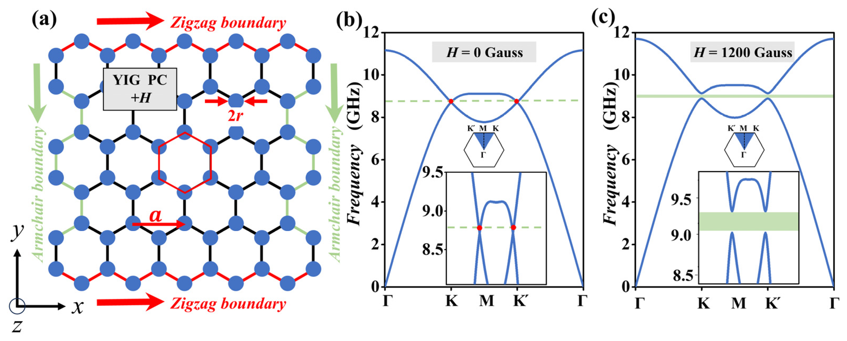
2.1. Basic GPC Structure

We start with a 2D honeycomb GPC which is composed of cylindrical yttrium iron garnet (YIG) rods immersed in air. As shown in Figure 1a, the relative permittivity and the radius of the YIG rods are ε = 14.5 and r = 0.15a, where a = 10 mm is the lattice constant of the GPC. The honeycomb GPC has two typical boundary configurations. One is the zigzag boundary along the x direction, while the other one is the armchair boundary along the y direction, as shown by the red and green arrows in Figure 1a, respectively. When no EMF is applied, the magnetic permeability of YIG rods is μ =1. However, when an EMF of H0 = +1200 Gauss is applied to the YIG rods along the +z direction, the gyromagnetic anisotropy is strongly induced to break time-reversal symmetry and the permeability becomes a tensor as follows [28,29]:
μ ^ = μ r j μ k 0 j u k μ r 0 0 0 1
where μr = 1 + ωm(ω0 + jαω)/[(ω0 + jαω)2ω2)] and μk = ωωm/[(ω0 + jαω)2ω2)], γ = 2.8 × 10⁶ Hz/Oe is the gyromagnetic ratio, ω0 = 2πf0 = 2πγH0 is the resonance frequency, ωm = 2πfm = 2πγM0 is the characteristic circular frequency, with M0 = 1750 Gauss being the saturation magnetization, and the damping coefficient is α = 3 × 10⁻⁴. The bulk band structures of transverse magnetic (TM) mode with H = 0 Gauss and +1200 Gauss are calculated by the honeycomb unit cell (marked as a red hexagon in Figure 1a) by the finite-element method, as shown in Figure 1b,c, respectively. In addition, all six boundaries of the unit cell are set into three pairs of parallel Floquet periodic boundaries.
Figure 1b is the bulk band structure of GPC without an EMF. Obviously, the band gap will not exist and in the first Brillouin zone, two bands couple with each other at two Dirac points of K and K’, which is marked as the green line intersecting with the band of two red dots. The larger image of Figure 1b shows that the frequencies of two Dirac points are 8.85 GHz. Figure 1c shows the bulk band structure of GPC, which is applied with H0 = +1200 Gauss. Two coupled points at Dirac points K and K’ are broken and the two bands are separated from each other (marked as the green zone). The larger image of Figure 1c shows that the opened band gap appears from 9.02 to 9.28 GHz with a bandwidth of 0.26 GHz.

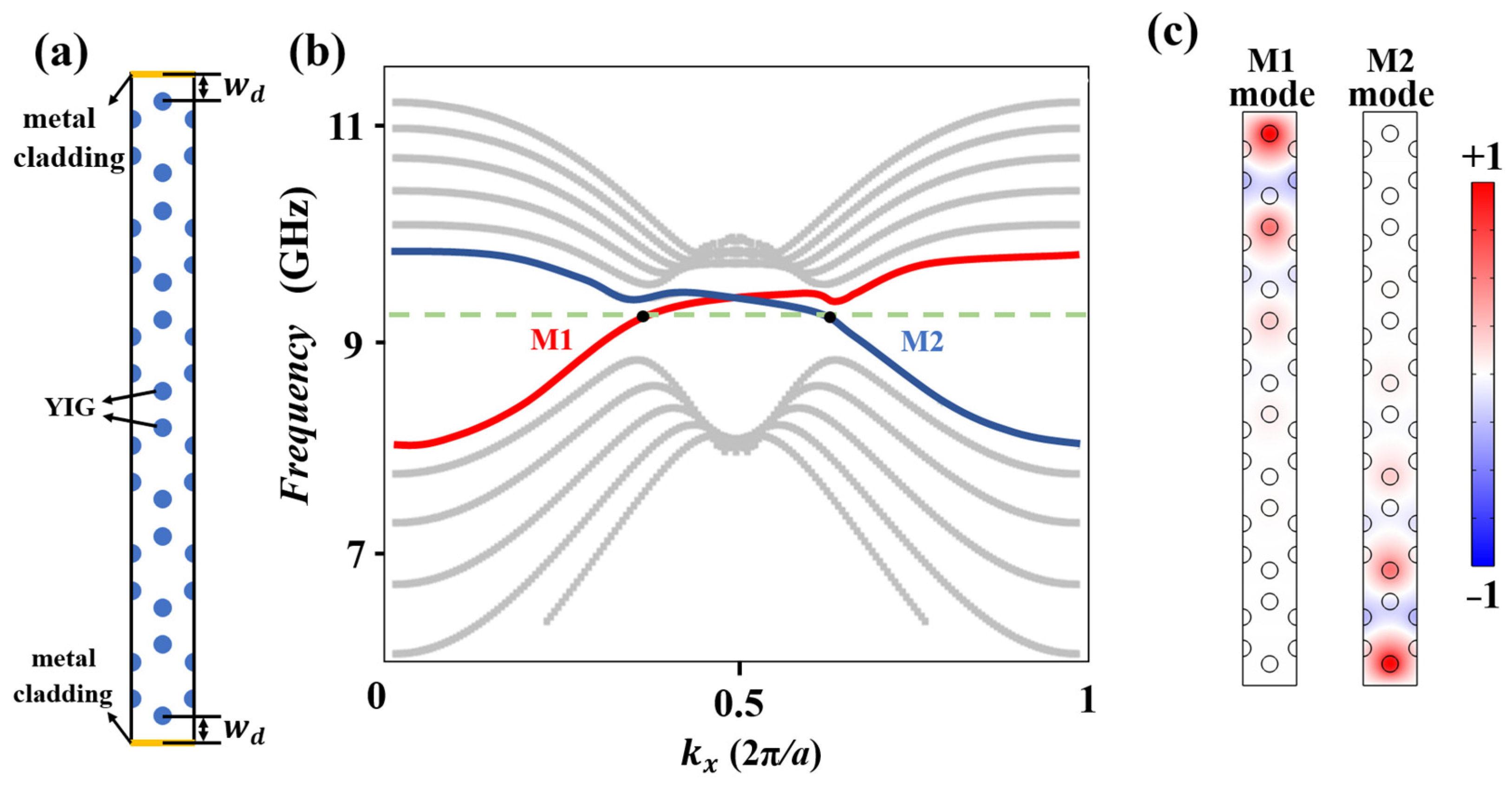
2.2. Projected Band Structure and Physical Mechanism Analysis

The Chern number Cn and the gap Chern number Cgap can describe the topological properties of the structure [28,30]. The above honeycomb GPC is applied with H0 = +1200 Gauss in Figure 1c. The Cn of the first and second bands are −1 and +1, respectively [31]. The sign of ΔCgap determines its propagation direction of the waveguide and the value of |ΔCgap| determines the number of one-way edge states.
Firstly, we study the characteristics of the projected band structure. To further explore the topological property, two metallic claddings (denoted by yellow color) are placed close to the zigzag edges of the 2D honeycomb GPC to form two isolated unilateral waveguides with a width of wd = a. Figure 2a shows the structure of supercell. It is remarkable that the upper and lower boundaries of the supercell are perfect electric conductors (PECs) which are used to avoid the energy leaking into the air. The left and right boundaries are Floquet periodic boundaries. Figure 2b shows the projected band structure of the upper and lower waveguides with ΔCgap of −1 and +1 (marked by red and blue line, respectively). There exists a topological band gap from 8.87 GHz to 9.50 GHz. The red and blue curves in the band gap represent two one-way edge states with counter-propagating directions. To demonstrate the characteristics of these waveguide modes in depth, we choose the central frequency (fs = 9.2 GHz) which intersects with the red and blue dispersion curves at points M1 and M2 for further discussions. Figure 2c shows the eigenmodal field of |E| of the M1 and M2 modes, respectively. Obviously, the eigenmodal fields are localized at the edges’ region and gradually decrease towards the center of the supercell.
Here, we discuss the physical mechanism of the extended one-way waveguide states. As shown in Figure 3a, we construct a supercell by the upper and lower PCs with opposite EMFs of +H and −H, respectively (mark by blue and red, respectively). The distance between the nearest red and blue cylinders is wd. As wd decreases from 1.5a to 0.35a, the band structures show evident differences, as shown in Figure 3(b1–b4). We take fs = 9.2 GHz for detailed analyses. When wd = 1.5a [Figure 3(c1)], the width of the waveguide is large enough so that the interaction between the upper and lower PCs is negligible. There only exists one edge state H2 and one transmission state H1. When wd decreases to 1a, the interaction effect between the upper and lower PCs appears and results in an even P1 mode and odd P2 mode, as well as a couple of degenerate antichiral edge states [i.e., P3(P4)] which co-propagate at the upper and lower boundaries of the structure. However, the odd P2 mode still mainly localizes at the center of the supercell, as shown in Figure 3(c2), meaning the interaction is not strong enough. Then, we continue to decrease the wd to observe the evolution of the eigenmodal field. Interestingly, when wd  0.5a, the width of the waveguide is small enough to cause a strong interaction; so, the odd mode and even mode both become the extended one-way waveguide states (Q1, Q4 for wd = 0.5a; R1, R4 for wd = 0.35a), as shown in Figure 3(c3,c4). In addition, the degenerate antichiral edge states (Q2, Q3) and (R2, R3) still exist. It is emphasized that for these extended waveguide states, their energy is no longer localized at the center of the supercell but spread throughout the entire structure. This property holds great potential in constructing a transmission structure with one-way large-area propagation, which is beneficial for enhancing spatial utilization. For simplification, we will choose the waveguide structure with wd = 0.35a for further discussions.

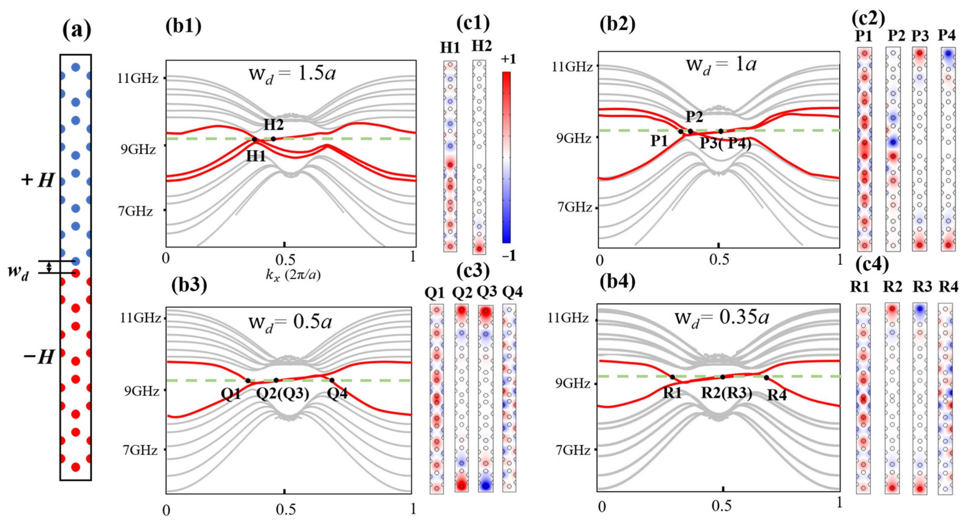
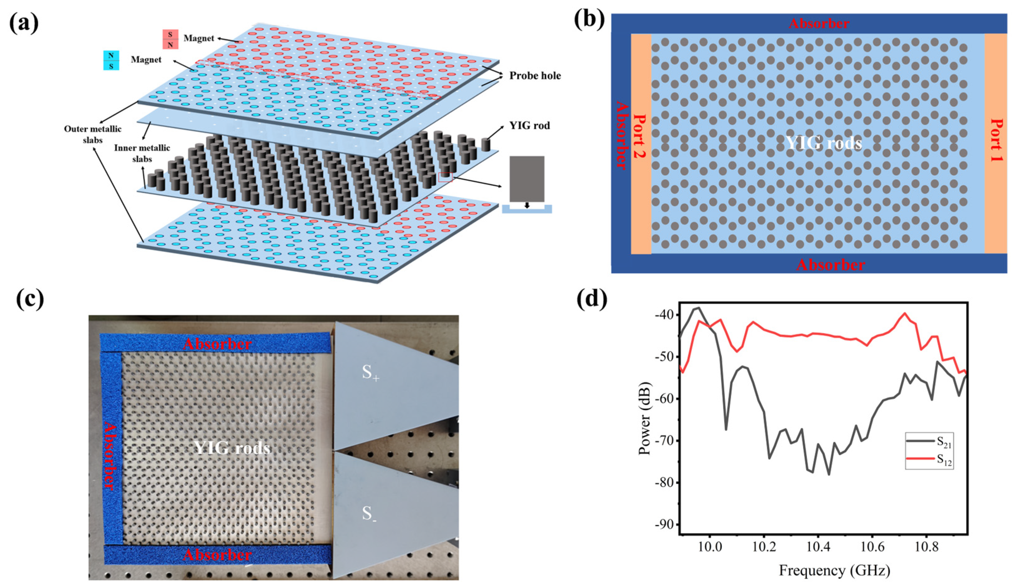
2.3. Design of Experiment Scheme

We theoretically analyzed the implementation of the extended one-way large-area waveguide states of honeycomb GPCs in detail. Here, we come up with a realistic experimental design to verify the simulation results. As shown in Figure 4a, the inner pair of metallic slabs are set in the upper and lower parts of the GPC structure to impede the electromagnetic waves from transporting in the z direction, while the outer pair of metallic slabs are carved out as honeycomb arrays to locate the magnet arrays, and then cover from the top and the bottom of the inner structure to complete sample fabrication. The positive and negative EMFs are produced by the different combinations of the magnetic poles of magnets (i.e., SN or NS combinations). Figure 4b shows the horizontal schematic diagram of the realistic experimental model for verifying the extended waveguide states. Three absorbers are set around the GPC structure to prevent the leakage of electromagnetic waves. The input port 1 and output port 2 (colored in the orange rectangles) are arranged on the right and left sides of the GPC structure. Figure 4c is the fabricated sample. We use vector network analyzer (Keysight P9374A, Santa Rosa, CA, USA) to observe the transmission of the signal. Two horn antennas (JUNCOAX-LB39591517, Shanghai, China) are used as two plane wave sources (marked with S+ and S−) with the same intensity but opposite phases at port 1 to excite the odd R4 mode. The transmission spectrum is measured and shown in Figure 4d. The topological band gap of the experiment appears from about 10.18 GHz to 10.66 GHz, meaning that the experimental band gap is slightly narrower than that in the simulation. This phenomenon is also affected by the uneven magnetization and the inaccurate geometric parameters of the YIG rods during fabrication. The red curve represents the energy ratio from port 1 to port 2, while the black curve is that from port 2 to port 1. They are marked as S12 and S21, respectively. The difference between the leftward and rightward transmissions between 10.18 and 10.66 GHz is 35 dB or so, exhibiting strong nonreciprocity, which can well satisfy practical needs. It should be noted that the topological band gap shifted about 1 GHz towards higher frequency since the magnetic field in the actual experiment is larger than that in the simulations.

3. Results

3.1. Numerical Simulations of the One-Way Large-Area Waveguide Extended States

In order to further explore the transmission behaviors of the extended one-way waveguide states of R1 and R4 modes, we construct a waveguide consisting of two identical GPCs with H0 = +1200 and −1200 Gauss as denoted by the yellow and black frames in Figure 5a, respectively. The size of the waveguide is 40a × 16 3 a. A series of 2D line sources (marked by stars) oscillating at fs = 9.2 GHz are placed at equal spacing on the right side of the structure, and they are longitudinally symmetrical regarding the waveguide, as shown in Figure 5a,b. The even R1 mode is excited when all line sources are in-phase. Conversely, the odd R4 mode is excited when the line sources on the upper and lower parts are in opposite phases. Figure 5a,b clearly shows that the R1 and R4 mode can propagate leftwards over a large area of the GPC rather than being localized within the waveguide, which is consistent with the eigenmodal field results in Figure 3(c3,c4). Being completely different from Figure 5a,b, when the line sources are placed on the left side of the GPC, the antichiral edge states of R2 and R3 are excited on the upper and lower boundaries of the GPC, respectively, and they co-propagate rightwards. These simulation results clearly demonstrate the different one-way transmission behaviors of these four waveguide modes [i.e., extended one-way waveguide states (R1, R4) and antichiral states (R2, R3)]. Figure 5d shows the amplitudes of electric field (|E|) of these four waveguide modes along the dotted green lines at x = 13.5a in Figure 5a–c. On the one hand, the |E| peaks of the R1 and R4 modes (colored in red and blue, respectively) are distributed near the waveguide with values of 9 × 10⁴ V/m and 7.5 × 10⁴ V/m, respectively. On the other hand, the |E| decreases slowly on both sides, showing the characteristics of Gaussian distribution. We can roughly estimate that the half-peak range is from y = 9.8a to 17.6a (marked by the green rectangle) with a width of 7.8a. In addition, it is worth noting that there exist two small peaks in the |E| curves of the R1 and R4 modes and their positions are consistent with the maximum peaks of the R2 and R3 modes (colored in dark green), indicating that the energy of the R1 and R4 modes diffuses to the upper and lower boundaries and slightly excites the antichiral R2 and R3 modes. It should be noted that the coupling strength between the even mode and antichiral modes is weaker than that between the odd mode and antichiral modes because the even mode decays faster than the odd mode along the y direction, as shown in Figure 5d.

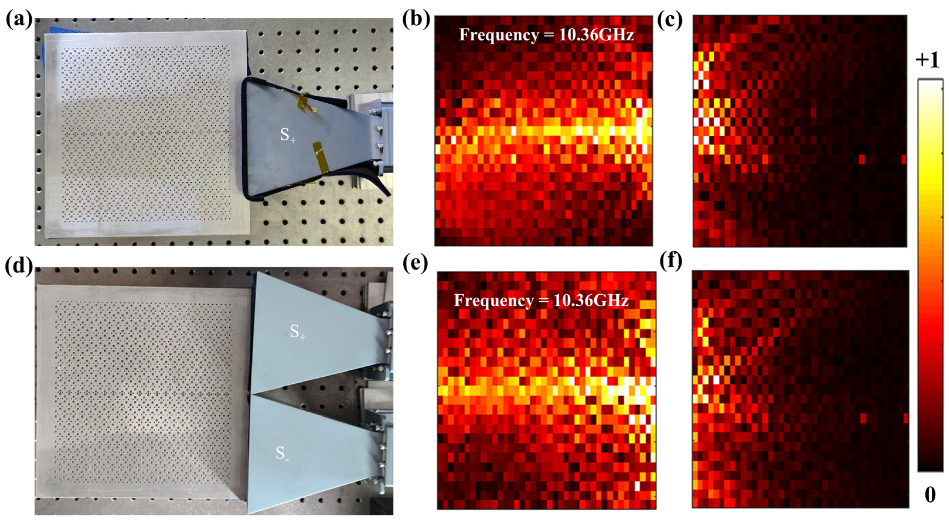
3.2. Experimental Results of the One-Way Large-Area Waveguide Extended States

Next, we carry out experiments to demonstrate the field distributions of both the even and odd extended waveguide states. The MATLAB program was used for data processing. The experiment setups and measured results are shown in Figure 6. The even and odd modes are excited by one plane wave source (S+) or two plane wave sources with opposite phases (S+ and S−), respectively (Figure 6a,c). In Figure 6b,e, we measure the field distributions of the R1 and R4 modes at 10.36 GHz by using the point-by-point scanning method. The experimental results demonstrate that they can both large-area propagate leftwards. Conversely, when the sources are placed on the left side of the structure, the measured results in Figure 6c,f clearly show that no electromagnetic wave can propagate rightwards. These experimental results prove that the structure supports excellent one-way large-area propagation of electromagnetic waves, which agrees well with the previous simulation results.

4. Conclusions

In conclusion, we realized the one-way large-area extended states in a GPC waveguide. When the width of the waveguide is small enough, the interaction between the upper and lower GPCs can create even and odd extended waveguide states simultaneously. They both support large-area one-way transmission within the topological band gap. Moreover, we demonstrated the large-area propagation phenomena of the even and odd states by microwave experiments. The simulated and the experimental results both prove the excellent large-area transmission performance of the proposed structure. Our work has improved the spatial utilization of the waveguide structure and paves the way for creating large-area one-way states. These excellent properties of such extended waveguide states support high-throughput transmission and the design of high-performance topological optical devices such as a Y-shaped splitter and a Z-shaped router. Moreover, the idea of extended one-way waveguide states can also be further extended to the visible or infrared light bands by reducing the lattice constant to the micro/nano scales with suitable materials.

Author Contributions

X.L. and C.Y. contributed to this work equally; conceptualization, and writing—original draft preparation, X.L. and C.Y. methodology, Z.-Y.L.; project administration and supervision, W.L. All authors have read and agreed to the published version of the manuscript.

Funding

This research was funded by the National Key R&D Program of China (2023YFA1406900); National Natural Science Foundation of China (12474380, 12074127); Natural Science Foundation of Guangdong Province (2023A1515010951); Education Teaching Reform Project of Guangdong (x2wl-C9233016).

Data Availability Statement

The data presented in this study are available on request from the corresponding author.

Conflicts of Interest

The authors declare no conflicts of interest.

References

  1. John, S. Strong Localization of Photons in Certain Disordered Dielectric Super Lattices. Phys. Rev. Lett. 1987, 58, 2486–2489. [Google Scholar] [CrossRef] [PubMed]
  2. Yablonovitch, E. Inhibited spontaneous emission in solid-state physics and electronics. Phys. Rev. Lett. 1987, 58, 2059–2062. [Google Scholar] [CrossRef] [PubMed]
  3. Haldane, F.D.M.; Raghu, S. Possible realization of directional optical waveguides in photonic crystals with broken time-reversal symmetry. Phys. Rev. Lett. 2008, 100, 013904. [Google Scholar] [CrossRef] [PubMed]
  4. Raghu, S.; Haldane, F.D.M. Analogs of quantum-Hall-effect edge states in photonic crystals. Phys. Rev. A 2008, 78, 033834. [Google Scholar] [CrossRef]
  5. Wu, L.-H.; Hu, X. Scheme for Achieving a Topological Photonic Crystal by Using Dielectric Material. Phys. Rev. Lett. 2015, 114, 223901. [Google Scholar] [CrossRef]
  6. Dong, J.W.; Chen, X.D.; Zhu, H.; Wang, Y.; Zhang, X. Valley photonic crystals for control of spin and topology. Nat. Mater. 2017, 16, 298–302. [Google Scholar] [CrossRef]
  7. Gao, F.; Xue, H.; Yang, Z.; Lai, K.; Yu, Y.; Lin, X.; Chong, Y.; Shvets, G.; Zhang, B. Topologically protected refraction of robust kink states in valley photonic crystals. Nat. Phys. 2017, 14, 140–144. [Google Scholar] [CrossRef]
  8. He, X.T.; Liang, E.T.; Yuan, J.J.; Qiu, H.Y.; Chen, X.D.; Zhao, F.L.; Dong, J.W. A silicon-on-insulator slab for topological valley transport. Nat. Commun. 2019, 10, 872. [Google Scholar] [CrossRef]
  9. Fukui, T.; Hatsugai, Y.; Suzuki, H. Chern Numbers in Discretized Brillouin Zone: Efficient Method of Computing (Spin) Hall Conductances. J. Phys. Soc. Jpn. 2005, 74, 1674–1677. [Google Scholar] [CrossRef]
  10. Bahari, B.; Ndao, A.; Vallini, F.; El Amili, A.; Fainman, Y.; Kante, B. Nonreciprocal lasing in topological cavities of arbitrary geometries. Science 2017, 358, 636–639. [Google Scholar] [CrossRef]
  11. Shao, Z.K.; Chen, H.Z.; Wang, S.; Mao, X.R.; Yang, Z.Q.; Wang, S.L.; Wang, X.X.; Hu, X.; Ma, R.M. A high-performance topological bulk laser based on band-inversion-induced reflection. Nat. Nanotechnol. 2020, 15, 67–72. [Google Scholar] [CrossRef] [PubMed]
  12. Zeng, Y.; Chattopadhyay, U.; Zhu, B.; Qiang, B.; Li, J.; Jin, Y.; Li, L.; Davies, A.G.; Linfield, E.H.; Zhang, B.; et al. Electrically pumped topological laser with valley edge modes. Nature 2020, 578, 246–250. [Google Scholar] [CrossRef] [PubMed]
  13. Liu, S.Y.; Lu, W.L.; Lin, Z.F.; Chui, S.T. Magnetically controllable unidirectional electromagnetic waveguiding devices designed with metamaterials. Appl. Phys. Lett. 2010, 97, 201113. [Google Scholar] [CrossRef]
  14. He, C.; Chen, X.L.; Lu, M.H.; Li, X.F.; Wan, W.W.; Qian, X.S.; Yin, R.C.; Chen, Y.F. Tunable one-way cross-waveguide splitter based on gyromagnetic photonic crystal. Appl. Phys. Lett. 2010, 96, 111111. [Google Scholar] [CrossRef]
  15. Tang, G.; Huang, Y.; Chen, J.; Li, Z.-Y.; Liang, W. A Topological Multichannel Add-Drop Filter Based on Gyromagnetic Photonic Crystals. Nanomaterials 2023, 13, 1711. [Google Scholar] [CrossRef]
  16. Tao, K.; Xiao, J.-J.; Yin, X. Nonreciprocal photonic crystal add-drop filter. Appl. Phys. Lett. 2014, 105, 211105. [Google Scholar] [CrossRef]
  17. Yan, C.; Huang, Y.; Li, Z.Y.; Liang, W. Controllable Pseudospin Topological Add-Drop Filter Based on Magnetic-Optical Photonic Crystals. Nanomaterials 2024, 14, 919. [Google Scholar] [CrossRef]
  18. Chen, J.F.; Liang, W.Y.; Li, Z.Y. Antichiral one-way edge states in a gyromagnetic photonic crystal. Phys. Rev. B 2020, 101, 214102. [Google Scholar] [CrossRef]
  19. Zhou, P.H.; Liu, G.G.; Yang, Y.H.; Hu, Y.H.; Ma, S.L.; Xue, H.R.; Wang, Q.; Deng, L.J.; Zhang, B.L. Observation of Photonic Antichiral Edge States. Phys. Rev. Lett. 2020, 125, 263603. [Google Scholar] [CrossRef]
  20. Yu, Z.; Veronis, G.; Wang, Z.; Fan, S. One-Way Electromagnetic Waveguide Formed at the Interface between a Plasmonic Metal under a Static Magnetic Field and a Photonic Crystal. Phys. Rev. Lett. 2008, 100, 023902. [Google Scholar] [CrossRef]
  21. Chen, J.; Li, Z.-Y. Configurable topological beam splitting via antichiral gyromagnetic photonic crystal. Opto-Electron. Sci. 2022, 1, 220001. [Google Scholar] [CrossRef]
  22. Chen, J.F.; Li, Z.Y. Prediction and Observation of Robust One-Way Bulk States in a Gyromagnetic Photonic Crystal. Phys. Rev. Lett. 2022, 128, 257401. [Google Scholar] [CrossRef] [PubMed]
  23. Wang, M.; Zhang, R.Y.; Zhang, L.; Wang, D.; Guo, Q.; Zhang, Z.Q.; Chan, C.T. Topological One-Way Large-Area Waveguide States in Magnetic Photonic Crystals. Phys. Rev. Lett. 2021, 126, 067401. [Google Scholar] [CrossRef]
  24. Qu, T.; Wang, N.; Wang, M.; Zhang, L.; Chen, J. Flexible electromagnetic manipulation by topological one-way large-area waveguide states. Phys. Rev. B 2022, 105, 195432. [Google Scholar] [CrossRef]
  25. Lan, Z.; Chen, M.L.N.; You, J.W.; Sha, W.E.I. Large-area quantum-spin-Hall waveguide states in a three-layer topological photonic crystal heterostructure. Phys. Rev. A 2023, 107, L041501. [Google Scholar] [CrossRef]
  26. Chen, Q.; Zhang, L.; Chen, F.; Yan, Q.; Xi, R.; Chen, H.; Yang, Y. Photonic Topological Valley-Locked Waveguides. ACS Photonics 2021, 8, 1400–1406. [Google Scholar] [CrossRef]
  27. Yu, X.; Chen, J.; Li, Z.-Y.; Liang, W. Topological large-area one-way transmission in pseudospin-field-dependent waveguides using magneto-optical photonic crystals. Photonics Res. 2023, 11, 1105–1112. [Google Scholar] [CrossRef]
  28. Wang, Z.; Chong, Y.D.; Joannopoulos, J.D.; Soljacic, M. Observation of unidirectional backscattering-immune topological electromagnetic states. Nature 2009, 461, 772–775. [Google Scholar] [CrossRef]
  29. Chen, J.F.; Liang, W.Y.; Li, Z.Y. Progress of Topological Photonic State in Magneto-Optical Photonic Crystal. Acta Opt. Sin. 2021, 41, 0823015. [Google Scholar]
  30. Skirlo, S.A.; Lu, L.; Igarashi, Y.C.; Yan, Q.H.; Joannopoulos, J.; Soljacic, M. Experimental Observation of Large Chern Numbers in Photonic Crystals. Phys. Rev. Lett. 2015, 115, 253901. [Google Scholar] [CrossRef]
  31. Zhao, R.; Xie, G.D.; Chen, M.L.N.; Lan, Z.; Huang, Z.; Sha, W.E.I. First-principle calculation of Chern number in gyrotropic photonic crystals. Opt. Express 2020, 28, 4638–4649. [Google Scholar] [CrossRef]
Figure 1. GPC structure and band structure. (a) The honeycomb GPC structure with the zigzag edges along the x direction. The unit cell (marked by red regular hexagon) is used to calculate the bulk band structures shown in (b,c). (b) The bulk band structure of TM mode without an EMF. The red dots indicate the two Dirac points which are connected by a green dotted line. (c) The bulk band structure of the TM mode with an EMF of H0 = +1200 Gauss. The green rectangle represents the band gap. The insets are the larger image of the band structure.
Nanomaterials 14 01790 g001
Figure 2. GPC supercell structure, band structure and eigenmodal fields. (a) The supercell of the honeycomb GPC structure which is used to calculate the projected band structure. Solid yellow lines at both sides indicate the metal claddings. (b) The projected band structure of TM mode with an EMF H0 = +1200 Gauss. A green dotted line represents a typical frequency of fs = 9.2 GHz, which intersects with two bands at M1 and M2 points, respectively. (c) The eigenmodal fields of M1 and M2 modes.
Nanomaterials 14 01790 g002
Figure 3. Schematic illustration, band structure and eigenmodal fields of the supercell. (a) Schematic illustration of the supercell. +H and −H are applied to the upper and lower cells (mark by blue and red, respectively). (b1b4) TM band structure for wd = 1.5a, 1a, 0.5a and 0.35a, respectively. (c1c4) Eigenmodal fields at 9.2 GHz with different wd.
Nanomaterials 14 01790 g003
Figure 4. (a) Three-dimensional schematic diagram of the realistic experimental model. The red and light-blue colors indicate different combinations of magnetic poles N and S. The white dots on the upper two metallic slabs represent the holes for probing the EM waves in the GPC structure. (b) Horizontal schematic diagram of the realistic experimental model. (c) The fabricated sample. (d) Transmission spectrum of the experiment structure.
Nanomaterials 14 01790 g004
Figure 5. Ez fields and the amplitude of electric fields (|E|). (ac) The intensity distributions of Ez fields of R1, R4, R2 and R3 modes, respectively. Stars of different color show the line sources are in opposite phases. (d) The amplitude of electric fields (|E|) along the green dotted lines of R1, R4, R2 and R3 modes, respectively. The green rectangle represents the half-peak range of electric fields.
Nanomaterials 14 01790 g005
Figure 6. Experimental setups and measured results. (a) Schematic diagram for the even R1 mode excited by S+. (b,c) The measured field distributions of the R1 mode at 10.36 GHz when the source is placed on the right and left side, respectively. (d) Schematic diagram for the odd R4 mode excited by S+ and S− with same intensity but opposite phases. (e,f) The measured field distributions of the R4 mode at 10.36 GHz when the sources are placed on the right and left side, respectively.
Nanomaterials 14 01790 g006
Disclaimer/Publisher’s Note: The statements, opinions and data contained in all publications are solely those of the individual author(s) and contributor(s) and not of MDPI and/or the editor(s). MDPI and/or the editor(s) disclaim responsibility for any injury to people or property resulting from any ideas, methods, instructions or products referred to in the content.

