
A Ku-Band Fully Differential Low-Power High-Input P1dB Low-Noise Amplifier


Abstract
1. Introduction
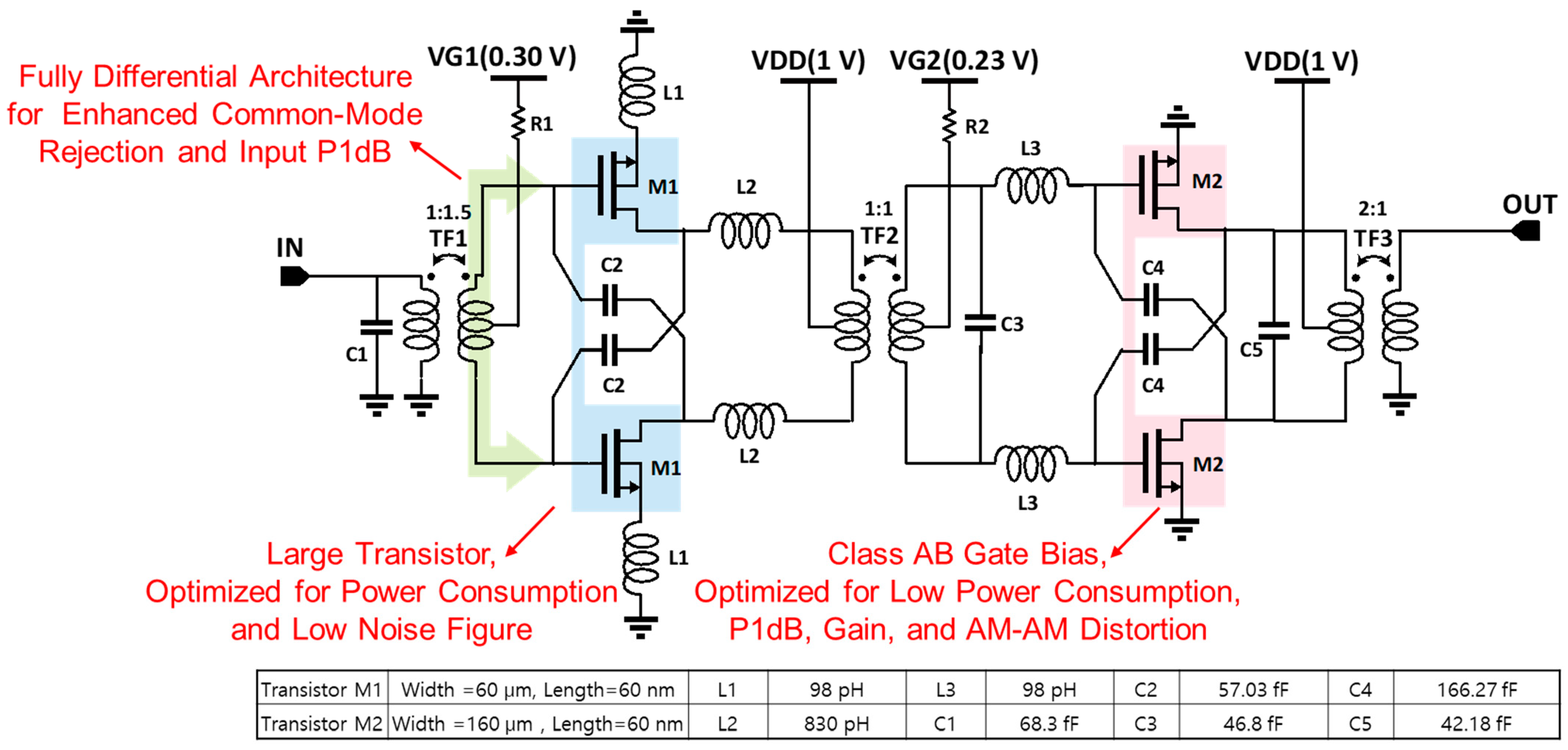
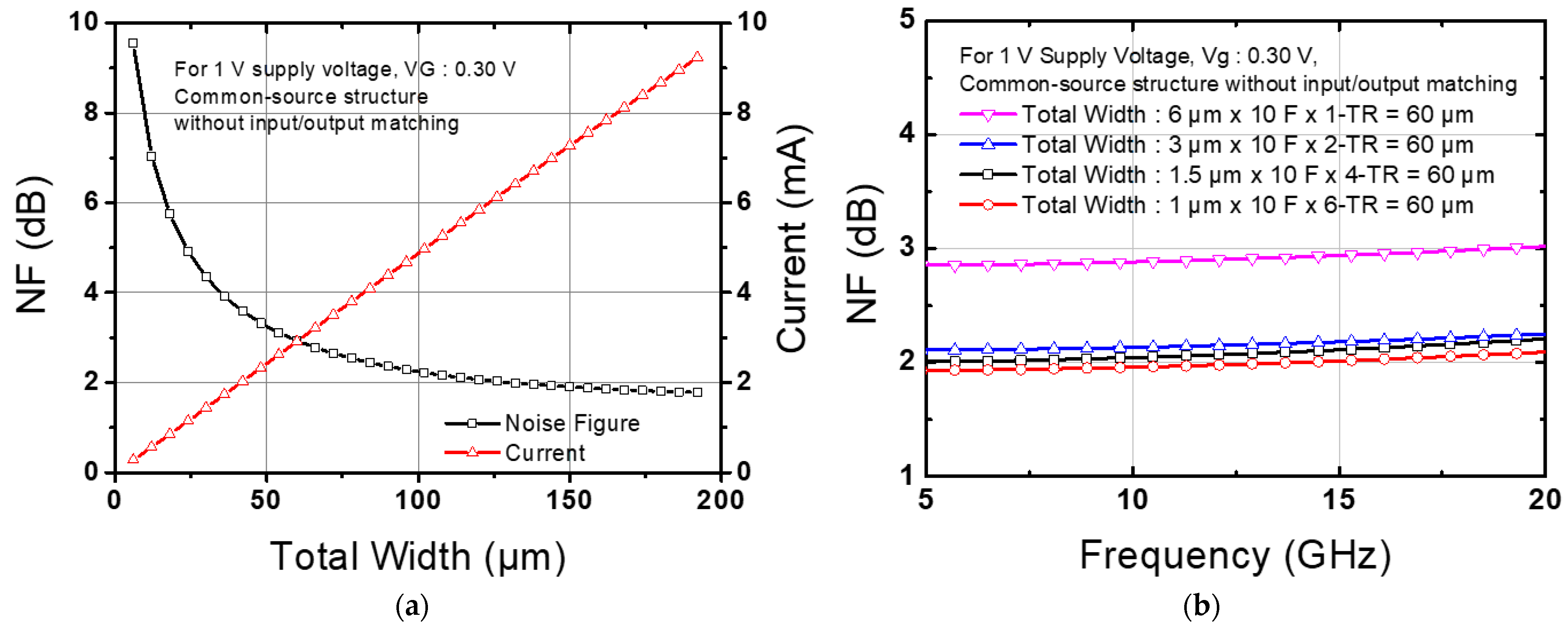
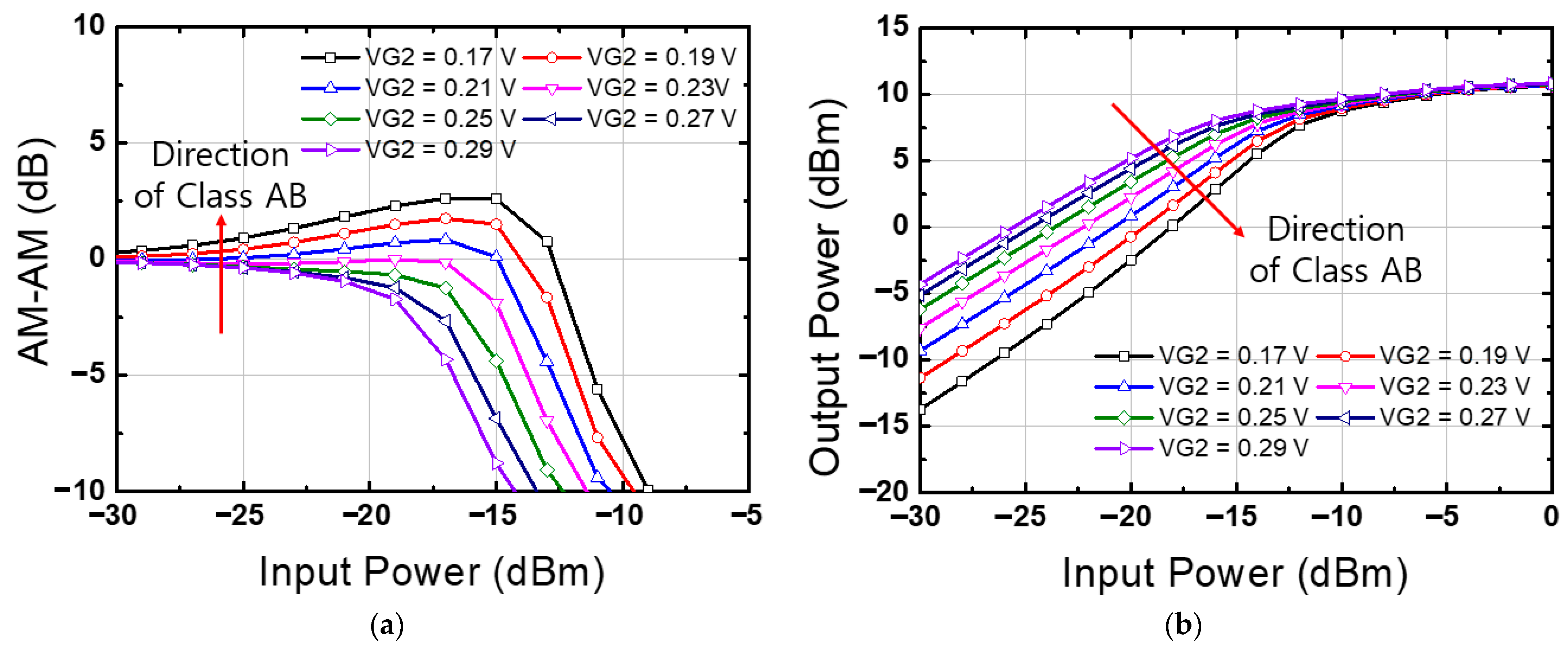
2. Circuit Design
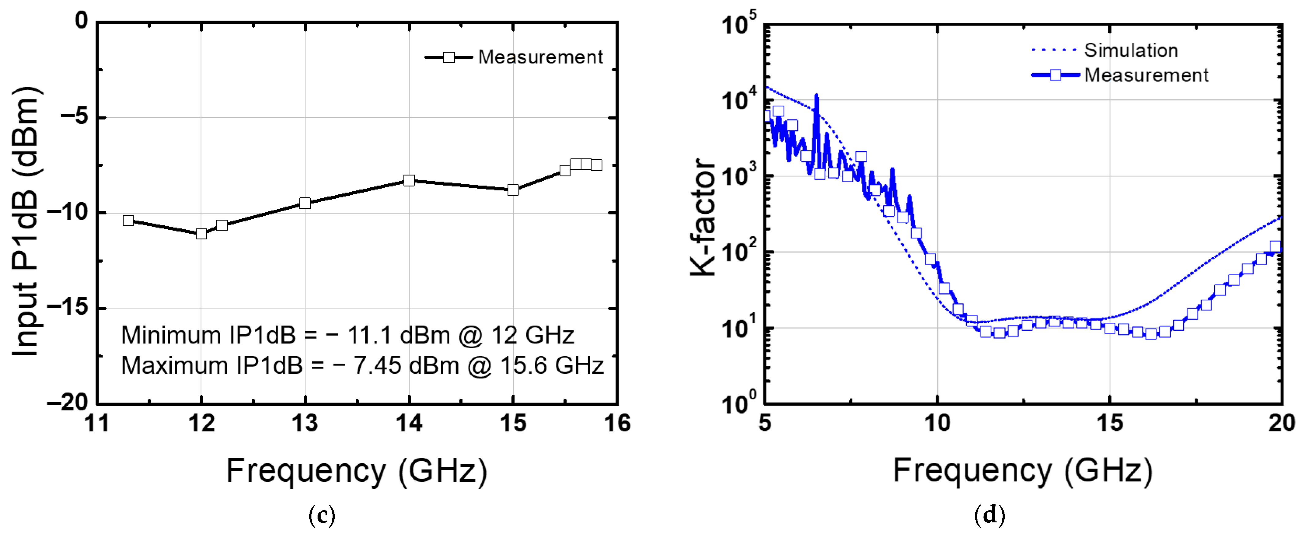
3. Measurement
4. Conclusions
Author Contributions
Funding
Data Availability Statement
Acknowledgments
Conflicts of Interest
References
- Golma, H.; Mogensen, P.; Viswanathan, H. Extreme Massive MIMO for Macro Cell Capacity Boost in 5G-Advanced and 6G; White Paper; Nokia Bell Labs: Murray Hill, NJ, USA, 2021. [Google Scholar]
- Semaan, E.; Tejedor, E.; Kochhar, R.K.; Magnusson, S. Realizing the 6G Vision—Why is Spectrum Fundamental? Erics-Son Blog 2022. Available online: https://www.ericsson.com/en/blog/2022/6/6g-spectrum-why-its-fundamental (accessed on 1 February 2023).
- Becoming 5G-Advanced: The 3GPP 2025 Roadmap. Available online: https://www.5gamericas.org/wp-content/uploads/2022/12/Becoming-5G-Advanced-the-3GPP-2025-Roadmap-InDesign.pdf (accessed on 1 February 2023).
- You, X.; Wang, C.X.; Huang, J.; Gao, X.; Zhang, Z.; Wang, M.; Liang, Y.C. Towards 6G wireless communication networks: Vision, enabling technologies, and new paradigm shifts. Sci. China Inf. Sci. 2021, 64, 110301. [Google Scholar] [CrossRef]
- 3GPP. Study on the 7–24 GHz Frequency Range for NR, Specification#: 38.820, Version 16.1.0. Available online: https://portal.3gpp.org/desktopmodules/Specifications/SpecificationDetails.aspx?specificationId=3599 (accessed on 1 February 2023).
- Kang, S.; Mezzavilla, M.; Rangan, S.; Madanayake, A.; Venkatakrishnan, S.B.; Hellbourg, G.; Ghosh, M.; Rahmani, H.; Dhananjay, A. Cellular Wireless Networks in the Upper Mid-Band. IEEE Open J. Commun. Soc. 2024, 5, 2058–2075. [Google Scholar] [CrossRef]
- Choi, H.-W.; Kim, C.-Y.; Choi, S. 6.7–15.3 GHz, High-Performance Broadband Low-Noise Amplifier with Large Transistor and Two-Stage Broadband Noise Matching. IEEE Microw. Wirel. Compon. Lett. 2021, 31, 949–952. [Google Scholar] [CrossRef]
- Peng, N.; Zhao, D. A Ku-Band Low-Noise Amplifier in 40-nm CMOS. In Proceedings of the 2019 IEEE International Conference on Integrated Circuits, Technologies and Applications (ICTA), Chengdu, China, 13–15 November 2019; pp. 9–10. [Google Scholar] [CrossRef]
- Chen, H.; Zhu, H.; Wu, L.; Xue, Q.; Che, W. A 7.2–27.3 GHz CMOS LNA with 3.51 ± 0.21 dB Noise Figure Using Multistage Noise Matching Technique. IEEE Trans. Microw. Theory Tech. 2021, 70, 74–84. [Google Scholar] [CrossRef]
- Qin, P.; Xue, Q. Design of Wideband LNA Employing Cascaded Complimentary Common Gate and Common Source Stages. IEEE Microw. Wirel. Compon. Lett. 2017, 27, 587–589. [Google Scholar] [CrossRef]
- Zhang, J.; Zhao, D.; You, X. A CMOS LNA with Transformer-Based Integrated Notch Filter for Ku-Band Satellite Communications. In Proceedings of the 2021 IEEE MTT-S International Microwave Symposium (IMS), Atlanta, GA, USA, 7–25 June 2021; pp. 592–594. [Google Scholar] [CrossRef]
- Inanlou, F.; Coen, C.T.; Cressler, J.D. A 1.0 V, 10–22 GHz, 4 mW LNA Utilizing Weakly Saturated SiGe HBTs for Single-Chip, Low-Power, Remote Sensing Applications. IEEE Microw. Wirel. Compon. Lett. 2014, 24, 890–892. [Google Scholar] [CrossRef]
- Zhang, C.; Wang, Y.; Gao, S.; Tang, L.; Zhang, Y.; Park, S.M. A switchable dual-mode fully-differential common-source low-noise amplifier in 0.18-μm CMOS technology. Microw. Opt. Technol. Lett. 2019, 62, 1163–1168. [Google Scholar] [CrossRef]
- Cruz-Acosta, J.M.; Galante-Sempere, D.; Khemchandani, S.L.; del Pino, J. A 0.38 V Fully Differential K-Band LNA with Transformer-Based Matching Networks. Appl. Sci. 2023, 13, 5460. [Google Scholar] [CrossRef]
- Choi, H.-W.; Choi, S.; Kim, C.-Y. Ultralow-Noise Figure and High Gain Ku-Band Bulk CMOS Low-Noise Amplifier with Large-Size Transistor. IEEE Microw. Wirel. Compon. Lett. 2021, 31, 60–63. [Google Scholar] [CrossRef]
- Yoon, J.; Park, C. A CMOS LNA Using a Harmonic Rejection Technique to Enhance Its Linearity. IEEE Microw. Wirel. Compon. Lett. 2014, 24, 605–607. [Google Scholar] [CrossRef]
- Kim, J.-H.; Son, J.-T.; Lim, J.-T.; Choi, H.-W.; Kim, C.-Y. Ultralow Noise Figure and Broadband CMOS LNA with Three-Winding Transformer and Large Transistor. IEEE Trans. Microw. Theory Tech. 2024, 72, 2734–2744. [Google Scholar] [CrossRef]
- Nguyen, T.-K.; Kim, C.-H.; Ihm, G.-J.; Yang, M.-S.; Lee, S.-G. CMOS low-noise amplifier design optimization techniques. IEEE Trans. Microw. Theory Tech. 2004, 52, 1433–1442. [Google Scholar] [CrossRef]
- Park, B.; Jin, S.; Jeong, D.; Kim, J.; Cho, Y.; Moon, K.; Kim, B. Highly Linear mm-Wave CMOS Power Amplifier. IEEE Trans. Microw. Theory Tech. 2016, 64, 4535–4544. [Google Scholar] [CrossRef]
- Chang, Y.-W.; Tsai, T.-C.; Zhong, J.-Y.; Tsai, J.-H.; Huang, T.-W. A 28 GHz Linear and Efficient Power Amplifier Supporting Wideband OFDM for 5G in 28 nm CMOS. In Proceedings of the 2020 IEEE/MTT-S International Microwave Symposium (IMS), Los Angeles, CA, USA, 4–6 August 2020; pp. 1093–1096. [Google Scholar] [CrossRef]
- Deng, Z.; Niknejad, A.M. A layout-based optimal neutralization technique for mm-wave differential amplifiers. In Proceedings of the 2010 IEEE Radio Frequency Integrated Circuits Symposium, Anaheim, CA, USA, 23–25 May 2010; pp. 355–358. [Google Scholar] [CrossRef]
- Asada, H.; Matsushita, K.; Bunsen, K.; Okada, K.; Matsuzawa, A. A 60 GHz CMOS power amplifier using capacitive cross-coupling neutralization with 16% PAE. In Proceedings of the 2011 6th European Microwave Integrated Circuit Conference, Manchester, UK, 10–11 October 2011; pp. 554–557. [Google Scholar]
- Chan, W.L.; Long, J.R. A 58–65 GHz Neutralized CMOS Power Amplifier with PAE Above 10% at 1-V Supply. IEEE J. Solid-State Circuits 2010, 45, 554–564. [Google Scholar] [CrossRef]


| Ref. | This Work | [7] | [8] | [9] | [10] | [11] | [12] |
|---|---|---|---|---|---|---|---|
| Technology | 65 nm CMOS | 65 nm CMOS | 40 nm CMOS | 65 nm CMOS | 65 nm CMOS | 65 nm CMOS | 130-nm SiGe |
| Supply Voltage [V] | 1 | 0.8 | 1 | 1.2 | 1 | 1 | 1 |
| Topology | Diff. (CS)-Diff. (CS) | Single (CS)-Single (CS) | Single (Cascode) | Single (CS)-Single (CC) | Single (CG)-Single (CS) | Single (CC)-Diff. (CS) | Single (CE)-Single (CE) |
| Frequency (GHz) | 11.24–15.89 | 6.7–15.3 | 10–14 | 7.2–27.3 | 7.6–29 | 9.2–12.7 | 10–22 |
| 3 dB-BW(GHz) | 4.65 | 8.6 | 4 | 20.1 | 21.4 | 3.5 | 12 |
| Peak Gain (dB) | 19.92 @ 12.2 GHz | 20 | 11 | 16.6 | 10.7 | 19.5 | 15.5 |
| Noise Figure Minimum (dB) | 2.7 @ 13.6 GHz | 2.08 (Average) | 1.7 | 3.3 | 4.5 | 2.3 | 3.2 |
| Input P1dB (dBm) | −7.45 @ 15.6 GHz | −17 | −8.8 | −11.7 | NA | −13.5 | NA |
| PDC (mW) | 11 | 12.8 | 10 | 13.2 | 12.1 | 5.9 | 4 |
| Core Area (mm2) | 0.26 | 0.144 | 0.162 | 0.14 | 0.3 | 0.8 | 0.1 |
| FoM I | 10.35 | 12.72 | 2.63 | 3.04 | 0.53 | 21.64 | 8.14 |
| FoM II | 1.86 | 0.25 | 0.35 | 0.21 | NA | 0.97 | NA |
Disclaimer/Publisher’s Note: The statements, opinions and data contained in all publications are solely those of the individual author(s) and contributor(s) and not of MDPI and/or the editor(s). MDPI and/or the editor(s) disclaim responsibility for any injury to people or property resulting from any ideas, methods, instructions or products referred to in the content. |
© 2024 by the authors. Licensee MDPI, Basel, Switzerland. This article is an open access article distributed under the terms and conditions of the Creative Commons Attribution (CC BY) license (https://creativecommons.org/licenses/by/4.0/).
Share and Cite
Lee, S.-R.; Kim, J.-H.; Baek, M.-S.; Kim, C.-Y. A Ku-Band Fully Differential Low-Power High-Input P1dB Low-Noise Amplifier. Nanomaterials 2024, 14, 1913. https://doi.org/10.3390/nano14231913
Lee S-R, Kim J-H, Baek M-S, Kim C-Y. A Ku-Band Fully Differential Low-Power High-Input P1dB Low-Noise Amplifier. Nanomaterials. 2024; 14(23):1913. https://doi.org/10.3390/nano14231913
Chicago/Turabian StyleLee, Sang-Rok, Joon-Hyung Kim, Min-Seok Baek, and Choul-Young Kim. 2024. "A Ku-Band Fully Differential Low-Power High-Input P1dB Low-Noise Amplifier" Nanomaterials 14, no. 23: 1913. https://doi.org/10.3390/nano14231913
APA StyleLee, S.-R., Kim, J.-H., Baek, M.-S., & Kim, C.-Y. (2024). A Ku-Band Fully Differential Low-Power High-Input P1dB Low-Noise Amplifier. Nanomaterials, 14(23), 1913. https://doi.org/10.3390/nano14231913