

Effect of Bias Voltage on the Microstructure and Photoelectric Properties of W-Doped ZnO Films


Abstract
:1. Introduction
2. Experimental Details
2.1. Coating Deposition
2.2. Coating Characterization
3. Results
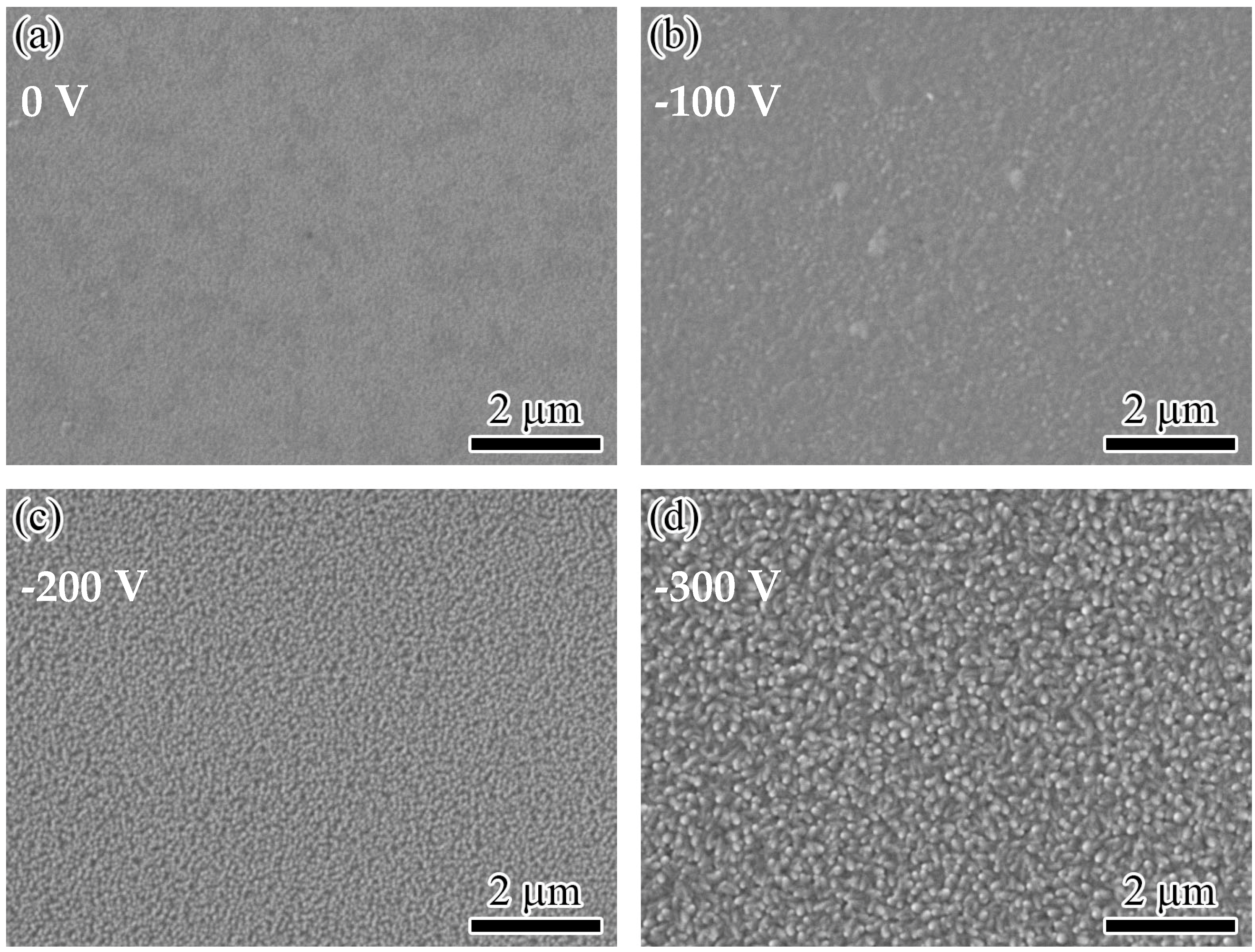
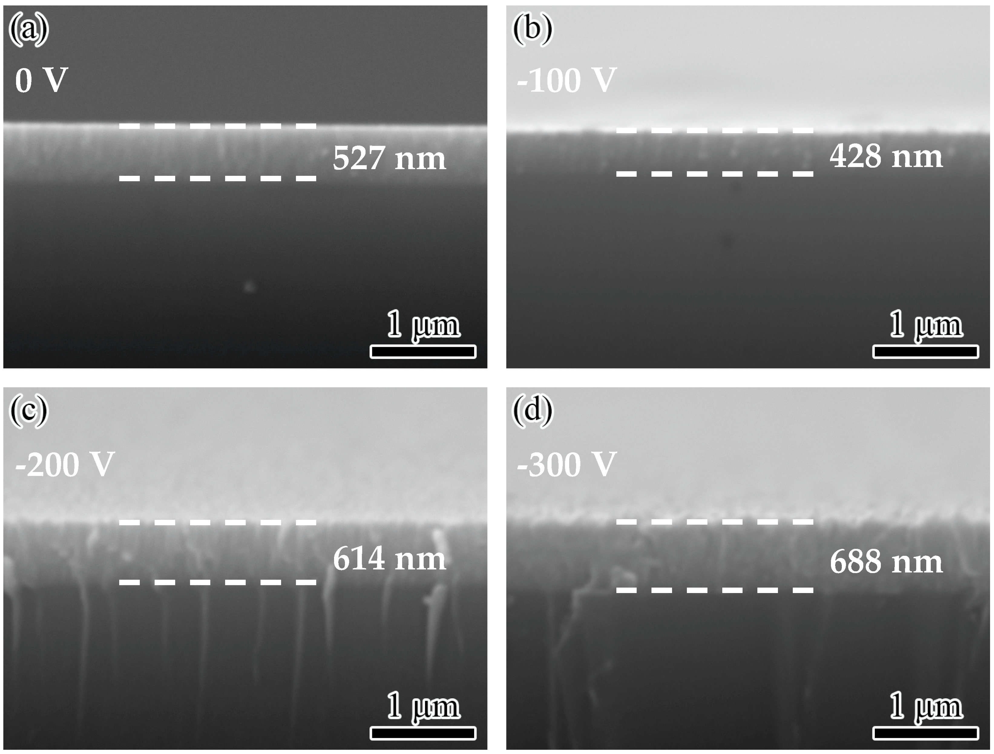
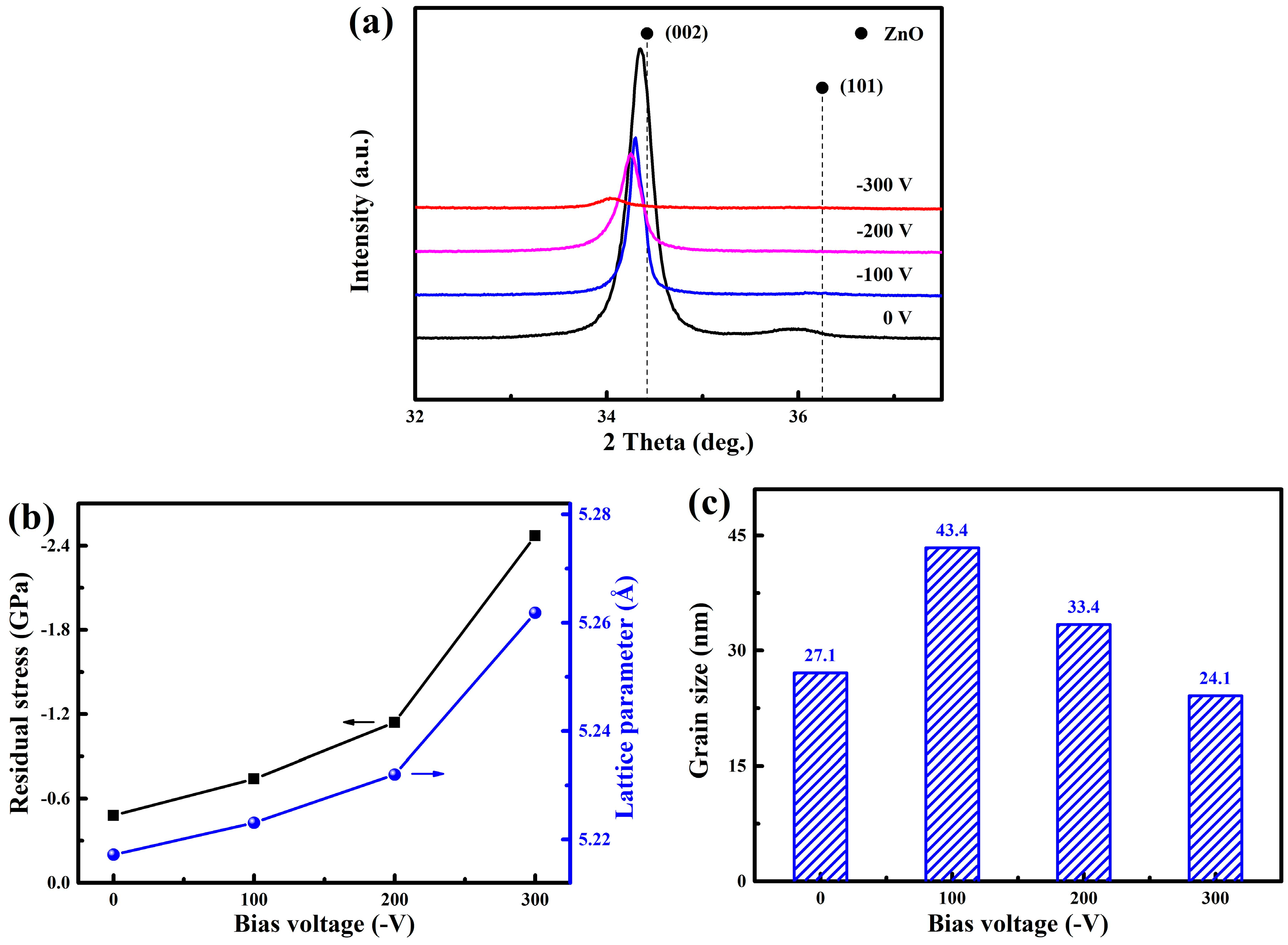
3.1. Microstructure
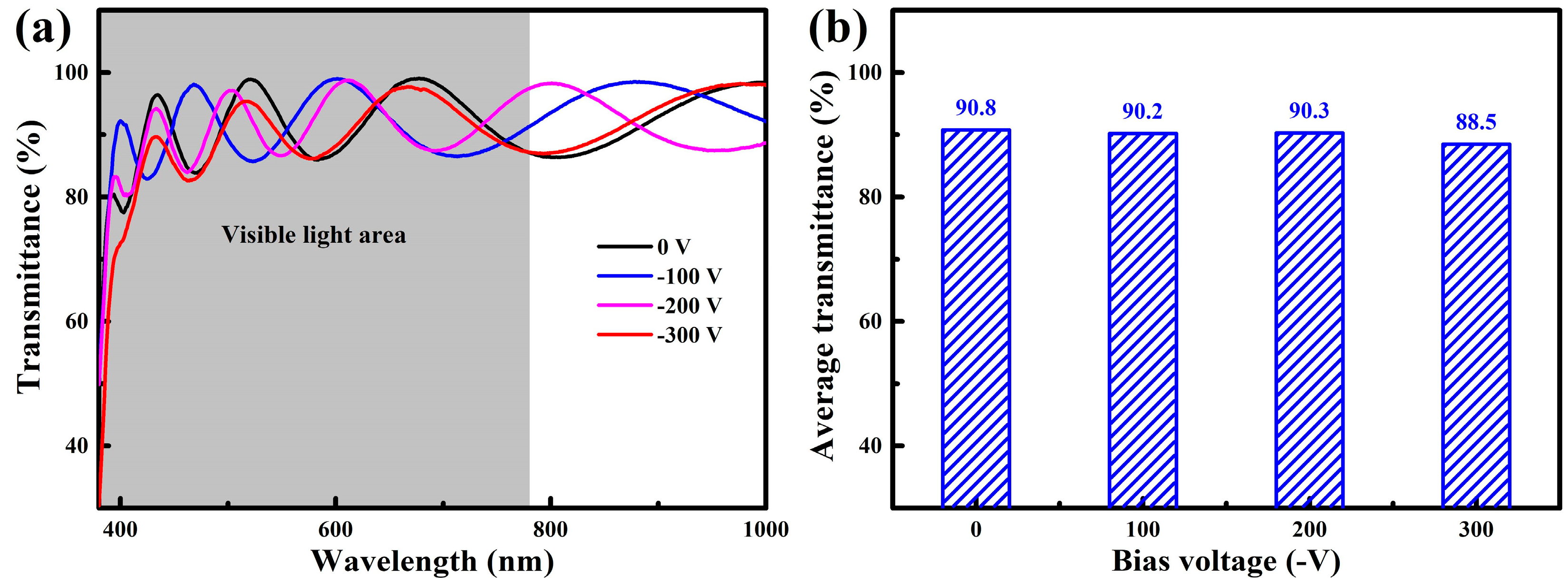
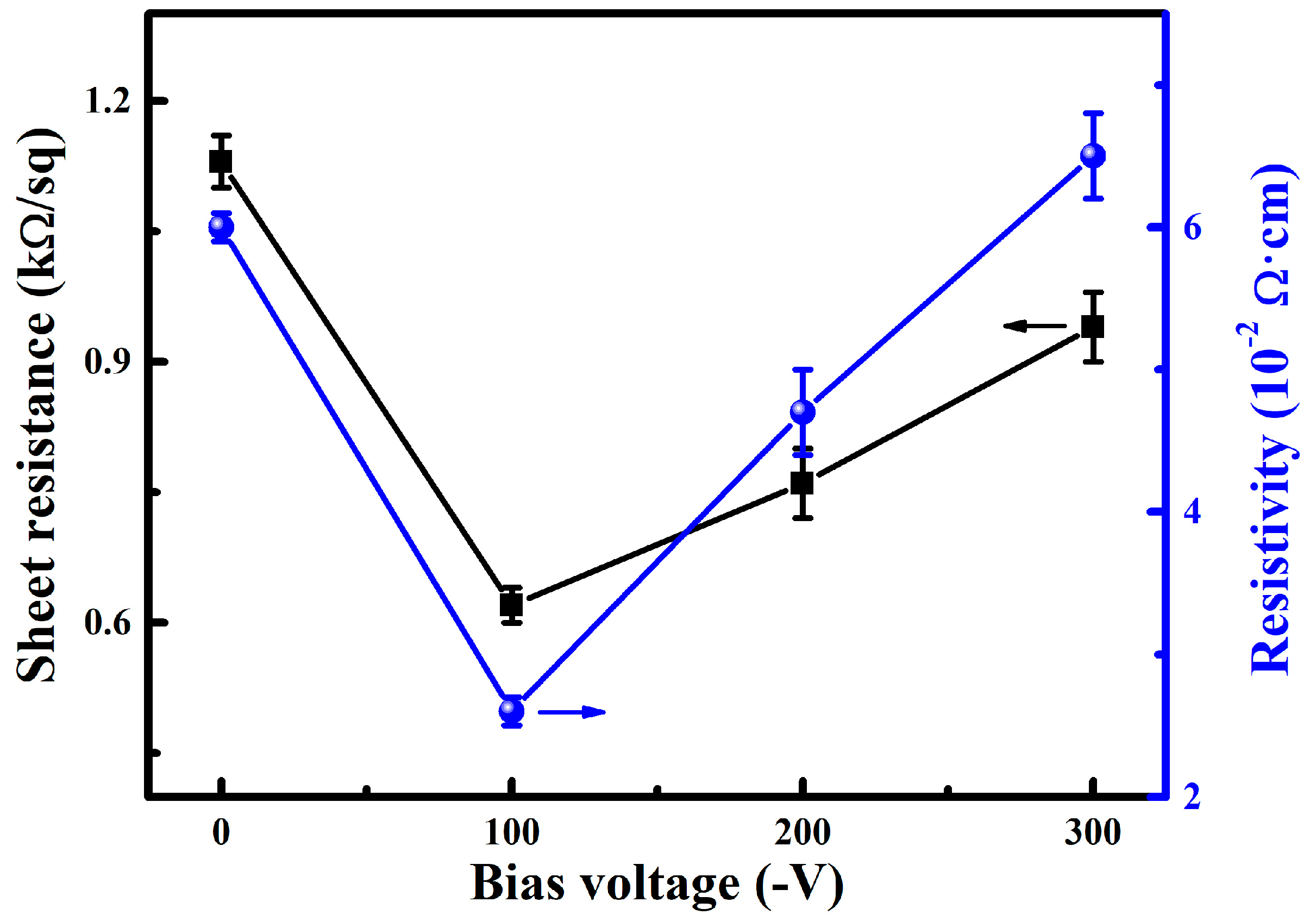
3.2. Photoelectric Properties
4. Conclusions
- (1)
- When the bias voltage increased from 0 to −300 V, the deposition rate of the films first decreased from 8.8 to 7.1 nm/min and then gradually increased to 11.5 nm/min. After applying bias voltage to the substrate, the ion bombardment effect was enhanced, and the surface morphology became much compact and rough.
- (2)
- All the WZO films exhibited a hexagonal wurtzite structure with a strong (002) preferred orientation, and grew along the c-axis direction. With an increasing bias voltage, the lattice parameter gradually increased from 5.2172 to 5.2618 Å, and the grain size first increased from 27.1 to 43.4 nm and then gradually decreased to 24.1 nm.
- (3)
- All the WZO films exhibited a high average transmittance of ~90% in the visible region. When the bias voltage was increased, the electrical resistivity of the films exhibited a trend of first decreasing and then increasing, and the highest FOM of 5.8 × 10⁻⁴ Ω−1 was achieved at −100 V.
Author Contributions
Funding
Data Availability Statement
Conflicts of Interest
References
- Lee, J.; Han, T.H.; Park, M.H.; Jung, D.Y.; Seo, J.; Seo, H.K.; Cho, H.; Kim, E.; Chung, J.; Choi, S.Y.; et al. Synergetic electrode architecture for efficient graphene-based flexible organic light-emitting diodes. Nat. Commun. 2016, 7, 11791. [Google Scholar] [CrossRef] [PubMed]
- Kim, H.M.; Geng, D.; Kim, J.; Hwang, E.; Jang, J. Metal-oxide stacked electron transport layer for highly efficient inverted quantum-dot light emitting diodes. ACS Appl. Mater. Interfaces 2016, 8, 28727–28736. [Google Scholar] [CrossRef] [PubMed]
- Tran, V.H.; Khan, R.; Lee, I.H.; Lee, S.H. Low-temperature solution-processed ionic liquid modified SnO2 as an excellent electron transport layer for inverted organic solar cells. Sol. Energy Mater. Sol. Cells 2018, 179, 260–269. [Google Scholar] [CrossRef]
- Hotovy, J.; Hüpkes, J.; Böttler, W.; Marins, E.; Spiess, L.; Kups, T.; Smirnov, V.; Hotovy, I.; Kováč, J. Sputtered ITO for application in thin-film silicon solar cells: Relationship between structural and electrical properties. Appl. Surf. Sci. 2013, 269, 81–87. [Google Scholar] [CrossRef]
- Bao, S.Y.; Deng, X.; Mao, F.; Zhong, N.; Yue, F.Y.; Sun, L.; Xiang, P.H.; Duan, C.G. Ultra-flat ITO films on mica for high temperature transparent flexible electrodes. Ceram. Int. 2020, 46, 2268–2272. [Google Scholar] [CrossRef]
- Liu, S.; Xu, X.; Jiang, J. Flexible transparent ITO thin film with high conductivity and high-temperature resistance. Ceram. Int. 2024, 50, 47649–47654. [Google Scholar] [CrossRef]
- Lung, C.; Toma, M.; Pop, M.; Marconi, D.; Pop, A. Characterization of the structural and optical properties of ZnO thin films doped with Ga, Al and (Al+Ga). J. Alloys Compd. 2017, 725, 1238–1243. [Google Scholar] [CrossRef]
- Mallick, A.; Basak, D. Revisiting the electrical and optical transmission properties of co-doped ZnO thin films as n-type TCOs. Prog. Mater. Sci. 2018, 96, 86–110. [Google Scholar] [CrossRef]
- Alev, O.; Özdemir, O.; Kılıç, A.; Akcan, D.; Büyükköse, S. Effect of Al doping on structural and optical properties of atomic layer deposited ZnO thin films. Surf. Interfaces 2024, 52, 104942. [Google Scholar] [CrossRef]
- Lemine, A.S.; Bhadra, J.; Popelka, A.; Shakoor, R.A.; Ahmad, Z.; Al-Thani, N.J.; Hasan, A. Synergistic effect of concentration and annealing on structural, mechanical, and room-temperature thermoelectric properties of n-type Ga-doped ZnO films. Ceram. Int. 2024, 50, 47741–47753. [Google Scholar] [CrossRef]
- Xing, L.; Lu, Y.; Liu, Y.; Wang, F.; Zhu, L.; Pan, X.; Ye, Z. Ga, Mg, F ternary-doped ZnO-based transparent conductive film prepared by radio-frequency sputtering with high transmittance. Mater. Lett. 2024, 360, 135972. [Google Scholar] [CrossRef]
- Shkir, M.; Khan, M.T.; Khan, A. Impact of Mo doping on photo-sensing properties of ZnO thin films for advanced photodetection applications. J. Alloys Compd. 2024, 985, 174009. [Google Scholar] [CrossRef]
- Ngom, B.D.; Mpahane, T.; Manyala, N.; Nemraoui, O.; Buttner, U.; Kana, J.B.; Fasasi, A.Y.; Maaza, M.; Beye, A.C. Structural and optical properties of nano-structured tungsten-doped ZnO thin films grown by pulsed laser deposition. Appl. Surf. Sci. 2009, 255, 4153–4158. [Google Scholar] [CrossRef]
- Ngom, B.D.; Sakho, O.; Manyala, N.; Kana, J.B.; Mlungisi, N.; Guerbous, L.; Fasasi, A.Y.; Maaza, M.; Beye, A.C. Structural, morphological and photoluminescence properties of W-doped ZnO nanostructures. Appl. Surf. Sci. 2009, 255, 7314–7318. [Google Scholar] [CrossRef]
- Abliz, A.; Wan, D.; Yang, L.; Mamat, M.; Chen, H.; Xu, L.; Wang, C.; Duan, H. Investigation on the electrical performances and stability of W-doped ZnO thin-film transistors. Mat. Sci. Semicon. Proc. 2019, 95, 54–58. [Google Scholar] [CrossRef]
- Zhang, H.F.; Liu, H.F.; Lei, C.X.; Yuan, C.K.; Zhou, A.P. Tungsten-doped ZnO transparent conducting films deposited by direct current magnetron sputtering. Vacuum 2010, 85, 184–186. [Google Scholar] [CrossRef]
- Zhang, C.; Chen, X.; Geng, X.; Tian, C.; Huang, Q.; Zhao, Y.; Zhang, X. Temperature-dependent growth and properties of W-doped ZnO thin films deposited by reactive magnetron sputtering. Appl. Surf. Sci. 2013, 274, 371–377. [Google Scholar] [CrossRef]
- Elmkhah, H.; Zhang, T.F.; Abdollah-zadeh, A.; Kim, K.H.; Mahboubi, F. Surface characteristics for the Ti-Al-N coatings deposited by high power impulse magnetron sputtering technique at the different bias voltages. J. Alloys Compd. 2016, 688, 820–827. [Google Scholar] [CrossRef]
- Ma, Q.; Li, L.; Xu, Y.; Gu, J.; Wang, L.; Xu, Y. Effect of bias voltage on TiAlSiN nanocomposite coatings deposited by HiPIMS. Appl. Surf. Sci. 2017, 392, 826–833. [Google Scholar] [CrossRef]
- Sekhar, M.C.; Reddy, N.N.K.; Reddy, B.P.; Prakash, B.P.; Akkera, H.S.; Uthanna, S.; Park, S.H. Influence of substrate bias voltage on crystallographic structure, optical and electronic properties of Al/(Ta2O5)0.85(TiO2)0.15/p-Si MIS Schottky barrier diodes fabricated by dc magnetron sputtering. Mat. Sci. Semicon. Proc. 2018, 76, 80–86. [Google Scholar] [CrossRef]
- Jiang, X.; Zeng, X.K.; Xie, W.; Liu, M.; Leng, Y.X. Optimizing substrate bias voltage to improve mechanical and tribological properties of ductile FeCoNiCu high entropy alloy coatings with FCC structure. J. Alloys Compd. 2024, 1004, 175972. [Google Scholar] [CrossRef]
- Tüzemen, E.S.; Eker, S.; Kavak, H.; Esen, R. Dependence of film thickness on the structural and optical properties of ZnO thin films. Appl. Surf. Sci. 2009, 255, 6195–6200. [Google Scholar] [CrossRef]
- Mendil, D.; Challali, F.; Touam, T.; Bockelée, V.; Ouhenia, S.; Souici, A.; Djouadi, D.; Chelouche, A. Preparation of RF sputtered AZO/Cu/AZO multilayer films and the investigation of Cu thickness and substrate effects on their microstructural and optoelectronic properties. J. Alloys Compd. 2021, 860, 158470. [Google Scholar] [CrossRef]
- Langford, J.I.; Wilson, A.J.C. Scherrer after sixty years: A survey and some new results in the determination of crystallite size. J. Appl. Crystallogr. 1978, 11, 102–113. [Google Scholar] [CrossRef]
- Chun, S.Y. Bias voltage effect on the properties of TiN films by reactive magnetron sputtering. J. Korean Phys. Soc. 2010, 56, 1134–1139. [Google Scholar] [CrossRef]
- Mei, H.; Yan, K.; Wang, R.; Cheng, L.; Li, Q.; Zhao, Z.; Ding, J.C.; Gong, W. Microstructure and mechanical properties of AlTiVCuN coatings prepared by ion source-assisted magnetron sputtering. Nanomaterials 2023, 13, 3146. [Google Scholar] [CrossRef]
- Windischmann, H. Intrinsic stress in sputter-deposited thin-films. Crit. Rev. Solid State 1992, 17, 547–596. [Google Scholar] [CrossRef]
- Wang, Y.P.; Lu, J.G.; Bie, X.; Ye, Z.Z.; Li, X.; Song, D.; Zhao, X.Y.; Ye, W.Y. Transparent conductive and near-infrared reflective Cu-based Al-doped ZnO multilayer films grown by magnetron sputtering at room temperature. Appl. Surf. Sci. 2011, 257, 5966–5971. [Google Scholar] [CrossRef]
- Wang, Y.; Zhang, X.; Huang, Q.; Wei, C.; Zhao, Y. Room temperature deposition of highly conductive and transparent hydrogen and tungsten co-doped ZnO films for thin film solar cells applications. Sol. Energy Mater. Sol. Cells 2013, 110, 94–97. [Google Scholar] [CrossRef]
- Zhang, H.; Yang, S.; Liu, H.; Yuan, C. Preparation and characterization of transparent conducting ZnO:W films by DC magnetron sputtering. J. Semicond. 2011, 32, 043002. [Google Scholar] [CrossRef]
- Zhang, D.; Sun, K.; Yin, H.; Cheng, L.; Yuan, H.; Yang, C. Optimization of photoelectric properties and temporal stability of AZO/Ti/Cu/AZO films by insertion of Ti layer for low emissivity applications. Mater. Sci. Eng. B 2023, 293, 116471. [Google Scholar] [CrossRef]
- Lv, M.; Xiu, X.; Pang, Z.; Dai, Y.; Han, S. Transparent conducting zirconium-doped zinc oxide films prepared by rf magnetron sputtering. Appl. Surf. Sci. 2005, 252, 2006–2011. [Google Scholar] [CrossRef]
- Haacke, G. New figure of merit for transparent conductors. J. Appl. Phys. 1976, 47, 4086–4089. [Google Scholar] [CrossRef]


| Parameters | |
|---|---|
| Base pressure (Pa) | 8.0 × 10⁻⁴ |
| Deposition temperature (°C) | 200 |
| Working pressure (Pa) | 0.5 |
| Ar flow rate (sccm) | 80 |
| Target-to-substrate distance (mm) | 115 |
| WZO target | ZnO:W = 98:2 wt% |
| Target power (W) | 150 |
| Substrate bias voltage (V) | 0, −100, −200, −300 |
| Deposition time (min) | 60 |
Disclaimer/Publisher’s Note: The statements, opinions and data contained in all publications are solely those of the individual author(s) and contributor(s) and not of MDPI and/or the editor(s). MDPI and/or the editor(s) disclaim responsibility for any injury to people or property resulting from any ideas, methods, instructions or products referred to in the content. |
© 2024 by the authors. Licensee MDPI, Basel, Switzerland. This article is an open access article distributed under the terms and conditions of the Creative Commons Attribution (CC BY) license (https://creativecommons.org/licenses/by/4.0/).
Share and Cite
Mei, H.; Wang, W.; Zhao, J.; Zhong, W.; Qiu, M.; Xu, J.; Gao, K.; Liu, G.; Liang, J.; Gong, W. Effect of Bias Voltage on the Microstructure and Photoelectric Properties of W-Doped ZnO Films. Nanomaterials 2024, 14, 2050. https://doi.org/10.3390/nano14242050
Mei H, Wang W, Zhao J, Zhong W, Qiu M, Xu J, Gao K, Liu G, Liang J, Gong W. Effect of Bias Voltage on the Microstructure and Photoelectric Properties of W-Doped ZnO Films. Nanomaterials. 2024; 14(24):2050. https://doi.org/10.3390/nano14242050
Chicago/Turabian StyleMei, Haijuan, Wanli Wang, Junfeng Zhao, Weilong Zhong, Muyi Qiu, Jiayang Xu, Kailin Gao, Ge Liu, Jianchu Liang, and Weiping Gong. 2024. "Effect of Bias Voltage on the Microstructure and Photoelectric Properties of W-Doped ZnO Films" Nanomaterials 14, no. 24: 2050. https://doi.org/10.3390/nano14242050
APA StyleMei, H., Wang, W., Zhao, J., Zhong, W., Qiu, M., Xu, J., Gao, K., Liu, G., Liang, J., & Gong, W. (2024). Effect of Bias Voltage on the Microstructure and Photoelectric Properties of W-Doped ZnO Films. Nanomaterials, 14(24), 2050. https://doi.org/10.3390/nano14242050