Article

Charge Transfer Mechanism in Type II WO3/Cu2O Heterostructure

Laboratory of Photoactive Nanocomposite Materials, Saint Petersburg State University, 199034 Saint-Petersburg, Russia
*
Author to whom correspondence should be addressed.
Nanomaterials 2024, 14(24), 2057; https://doi.org/10.3390/nano14242057
Submission received: 24 November 2024 / Revised: 16 December 2024 / Accepted: 20 December 2024 / Published: 23 December 2024
(This article belongs to the Section Nanoelectronics, Nanosensors and Devices)

Abstract

:
In this study, we explore the charge transfer mechanism between WO3 and Cu2O in heterostructured WO3/Cu2O electrodes and in a WO3||Cu2O tandem photoelectrochemical cell. The physical–chemical characterizations of the individual WO3 and Cu2O electrodes and the heterostructured WO3/Cu2O electrode by XRD, XPS, and SEM methods confirm the successful formation of the target systems. The results of photoelectrochemical studies infer that in both the heterostructured WO3/Cu2O electrode and WO3||Cu2O tandem photoelectrochemical cell, the major mechanism of charge transfer between WO3 and Cu2O is a realization of the Z-scheme.

1. Introduction

In recent years, photoactive materials forming type II heterostructures have been considered as perspective systems for the development of the “green” technology of photochemical solar energy conversion to produce “solar fuel”—either hydrogen from water splitting or higher energy products of carbon dioxide reduction [1,2,3,4,5,6,7]. Type II heterostructures consist of two semiconductor components (SCs), in which energy bands are shifted relative to each other in energy, and the valence band (VB) and the conduction band (CB) of the first SC are located above the corresponding bands of the second SC (see Figure 1).
The major advantage of type II heterostructures consisting of two components compared to conventional single-component photoactive materials is their ability for spatial charge separation between heterostructure components (see Figure 1). This effect results in the decay of charge carrier recombination efficiency and the accumulation of a higher density of both electrons and holes in corresponding components of the heterostructure, which, in turn, increase the probability of multielectron redox reactions, such as water splitting and CO2 reduction [7,8]:
  • 2H2O + 4e → H2 + 2OH;
  • 2H2O + 4h+ → O2 + 4H+;
  • CO2 + 4e + 4H+ → HCHO + H2O;
  • CO2 + 6e + 6H+ → CH3OH + H2O;
  • CO2 + 8e + 8H+ → CH4 + 2H2O.
In general, there are two different possible mechanisms of charge separation at the heterojunction of the type II heterostructure: the conventional type II mechanism, when electrons transfer from the CB of SC1 to the CB of SC2 and holes migrate from the VB of SC2 to the VB of SC1, and the Z-scheme mechanism, when electrons from the CB of SC2 recombine at the heterojunction with holes in the VB of SC1 (see Figure 1). A distinguished advantage of the Z-scheme compared to the conventional type II mechanism is that the total driving force |∆G| to initiate redox reactions in the Z-scheme is higher than the corresponding driving forces of individual components, whereas for the conventional type II mechanism, the total driving force of the heterostructure is less than the driving forces of individual components (see Figure 1). For example, to split water, the CB of the SC must be located at a potential more negative than the H+/H2 reduction potential, while the VB must be more positive than the oxidation potential H2O/O2 (1.23 V relative to the normal hydrogen electrode) [9]. In this context, the extended range of the heterostructure total driving force allows for more redox reactions to be initiated. This makes heterostructures realizing the Z-scheme mechanism more favorable as heterostructured photoactive materials.
To date, numerous studies have been performed to establish charge separation mechanisms in various type II heterostructured photoactive materials, reporting the realization of either conventional or Z-scheme mechanisms. Surprisingly, in different studies, both mechanisms were observed for the same heterostructured materials [7,10,11,12,13,14,15,16,17]. Thus, one can assume that, in general, both mechanisms can be realized in the type II heterostructure at the same time, and which mechanism becomes dominant is dictated by the spatial construction of the heterostructure and photoexcitation conditions as well as by the type of redox processes [7,14,15,16,17,18].
To establish how photoexcitation conditions affect the type of charge separation mechanism at the type II heterojunction, in this study, we explored a heterostructure formed by WO3 and Cu2O in a photoelectrochemical water-splitting reaction. In addition, we also performed studies of photoelectrochemical behavior in a tandem photoelectrochemical cell with tungsten oxide acting as a photoanode and copper(I) oxide being a photocathode. The selection of these two components of the heterostructure is dictated by their well-established electronic and photoelectrochemical properties [19,20,21,22].
WO3 is an n-type SC with a band energy of about 2.7–2.9 eV and a sufficiently high oxidation potential of holes, making tungsten oxide a promising visible-light-active material [19,20]. However, the reduction potential of tungsten oxide is insufficient to initiate most of the desired reduction processes. Moreover, the photo-corrosion of WO3 during the water-splitting process was evidenced [23,24]. At the same time, a combination of WO3 with a complementary semiconductor with high reduction potential might lead to the creation of an efficient redox system in either photocatalytic or photoelectrochemical systems [25].
The role of such complementary semiconductors can be particularly performed by copper(I) oxide, Cu2O. Cu2O is a narrow band gap p-type semiconductor with a band gap of about 2.1 eV [21]. It has a higher reduction potential than that of WO3, which makes it an effective photocathode for the photoelectrochemical water-splitting process. However, under irradiation, it can suffer from both self-oxidation, forming copper oxide (CuO), and self-reduction, forming metallic copper (Cu) [21,22].
In spite of the limitations of employing a single-component WO3 and Cu2O photocatalysts, their combination demonstrated higher activity in both photocatalytic [26,27,28,29] and photoelectrochemical [16,17,30,31,32,33,34] processes. It was shown that p-Cu2O/n-WO3 coupling helps to avoid photoinduced charge back reactions in the photoelectrochemical water-splitting process, which results in increased photocatalytic hydrogen production and improved stability of both WO3 and Cu2O materials [16,17,32,33,34]. The Z-scheme mechanism of charge transfer through the Cu2O/WO3 heterojunction resulting in the photoinduced water-splitting process was considered in [16,32,33], while in other studies [17,34], it was associated with a conventional type II charge transfer mechanism.
The results of the operation of a tandem photoelectrochemical cell (PEC) with a WO3 photoanode and a Cu2O|NiOx photocathode confirm the possibility of water splitting without external bias with conversion efficiency achieving about 0.22% under 1 Sun irradiation [35]. The photoelectrochemical behavior of the ITO/WO3/Cu2O/CuO heterostructured electrode demonstrates an efficiency improved by approximately 5.5 times compared to ITO/WO3 due to, as assumed, the conventional type II heterojunction charge separation mechanism [17]. In [36], the charge transfer mechanism in the heterostructure Cu/Cu2O/WO3 was assumed to coincide with the S-scheme mechanism (a modification of the Z-scheme). Thus, currently, there is no well-established dominating mechanism of charge separation and transfer in the WO3/Cu2O heterostructure.
In this study, we explore the possibility of charge transfer mechanism variation at heterojunctions depending on the photoexcitation conditions of the planar WO3/Cu2O heterostructure.

2. Materials and Methods

A tungsten (VI) oxide electrode was prepared by the drop-casting of a stable transparent tungsten alcoholate sol. To form the alcoholate sol, tungsten (VI) chloride (≥99.9%, Vekton, Saint-Petersburg, Russia) in an amount of 1 g (2.52 mmol) was dissolved in 20 mL of purified isopropyl alcohol (≥99.0%, Vekton, Saint-Petersburg, Russia) with the addition of 2 mL of glacial acetic acid (60.05 g/mol, Vekton, Saint-Petersburg, Russia). The obtained product was stirred for 30 min, after which 2 mL of concentrated hydrogen peroxide solution (60%, NevaReaktiv, Saint-Petersburg, Russia) was added, and the solution was left stirring for 12 h. After aging, the sol solution was available for synthesis of WO3 films for one week.
The films were obtained by uniformly distributing the sol onto a conducting fluorine-doped tin oxide (FTO, 25 mm × 25 mm and a surface resistance of <100 Ohm/cm) substrate surface at room temperature, followed by removing the solvent at 60 °C for 1 h and further annealing the films at 350 °C for 1 h. The heating speed was 60°/h, and the cooling speed was arbitrary. The thickness of the tungsten oxide layer (VI) could be varied by the volume of the applied sol. In operation, the sol volume was 120 μL per 25 mm × 25 mm FTO substrate. The substrates were pre-cleaned by an ultrasonic bath treatment in an aqueous detergent solution, then in isopropyl alcohol, followed by annealing at 450 °C for 30 min.
The Cu2O films were prepared by electrodeposition on pre-cleaned conducting FTO substrates from an aqueous solution containing sodium acetate (0.1 M) (99.9%, NevaReaktiv, Saint-Petersburg, Russia) and copper acetate (0.1 M) (99.9%, NevaReaktiv, Saint-Petersburg, Russia). The film deposition process was carried out in a three-electrode electrochemical cell in potentiostatic mode using an Elins-Pro potentiostat (LLC “Elins”, Moscow, Russia) while applying a potential of −0.245 V with respect to the potential of the Ag/AgCl reference electrode (OhmLiberScience, Saint-Petersburg, Russia) for 10 min; a platinum plate (OhmLiberScience, Saint-Petersburg, Russia) was used as the counter electrode. After deposition, the thin layer substrate was washed with distilled water, air dried to remove visible water residues, and annealed in a furnace (LOIP LTD, Saint-Petersburg, Russia) at 300 °C for 5 min, followed by rapid cooling down to room temperature.
Planar “layer-by-layer” heterostructured electrodes were prepared using the methods of synthesis and formation of the corresponding material films based on the preparation methods developed for the individual compounds. The formation of the upper Cu2O layer as a component of the heterostructure was also carried out by electrodeposition on a stable WO3 film with the same conditions as described above, to form FTO/WO3/Cu2O heterostructured electrodes. The formation of the heterostructure with an opposite architecture, FTO/Cu2O/WO3, was not successful since at the heating conditions required to form the WO3 layer, the formation of CuWO4 takes place.
The surface morphology of the samples was studied using scanning electron microscopy (SEM) with a Zeiss SUPRA 40VP microscope (Carl Zeiss, Oberkochen, Germany). The phase composition of electrodes was determined by X-ray diffraction with a Bruker “D8 DISCOVER” high-resolution diffractometer (Bruker AXS GmbH, Karlsruhe, Germany) applying CuKa radiation in the angle range 20° ≤ 2θ ≤ 80° with a scanning speed of 5.0°/min. The phase reference data were taken from the ICDD database. A Thermo Fisher Scientific Escalab 250Xi spectrometer (Brighton, UK) was used for the registration of both the X-ray Photoelectron Spectroscopy (XPS) and UV Photoelectron Spectroscopy (UPS) spectra.
Electrochemical measurements were performed in a three-electrode electrochemical cell using an Elins-50 Pro potentiostat (LLC “Elins”, Moscow, Russia). The platinum plate and Ag/AgCl electrode were used as the counter electrode and reference electrode, respectively. A 0.2 M aqueous solution of potassium sulfate (pH 6.98, Vekton, Saint-Petersburg, Russia) was used as an electrolyte. The scanning speed for volt–current dependences was 15 mV/s. The Mott–Schottky dependences were registered at 1000 Hz. The spectral dependences of the photocurrent were performed using a home-made two-electrode electrochemical cell with a Pt counter electrode (OhmLiberScience, Saint-Petersburg, Russia).
Photoelectrochemical studies were performed with irradiation by a 300 W Xenon Lamp (Oriel Instruments, Darmstadt, Germany). The light intensity in the visible spectral range applying a cut-off filter JS-11 (Vavilov SOI, Saint-Petersburg, Russia), with a transmittance edge at 410 nm, was 320 mW/cm2. The spectral dependences of the photocurrent were measured with monochromator MDR-2 (LOMO, Saint-Petersburg, Russia).

3. Results and Discussion

3.1. Physical–Chemical Characterization

The surface morphology and side view of the electrodes are shown in Figure S1. The surface of the Cu2O electrode consists of agglomerates of microparticles with a size larger than 1 µm, densely adjoining each other. The WO3 surface is represented by particles larger than 100 nm, forming a dense layer with a developed surface due to protruding faces of crystallites. The heterostructure FTO/WO3/Cu2O is characterized by a dense surface morphology, similar to the Cu2O phase, and is approximately 0.9 µm in total thickness, composed of individual layers of Cu2O with a thickness of 0.4 µm and a WO3 layer with a thickness 0.5 µm.
Phase compositions of all the electrodes were characterized by XRD phase analysis. XRD analysis of the electrodes containing Cu2O confirmed the presence of the copper(I) oxide phase (card #01-071-3645). It is known that copper(I) compounds can be easily oxidized to copper(II) compounds, and on the conducting substrate, Cu2O can recover to metal copper [37,38]. The XRD data shown in Figure S2 demonstrate the absence of both the CuO and Cu phases. The XRD analysis of electrodes based on tungsten oxide revealed the formation of a monoclinic phase WO3 with a spatial group P21/N, as presented in Figure S2. For the heterostructured FTO/WO3/Cu2O electrode, it is shown that the applied methods of heterostructure formation preserve the phase composition of the individual components (Figure S2).
The chemical composition and the oxidation states of the elements were studied by the XPS method. The survey spectra for all electrodes are presented in Figure S3. The main peaks related to the binding energy (BE) of ~933.5 eV, ~38.0 eV and ~529.7 eV correspond to Cu2p, W4f, and O1s, respectively, indicating the expected chemical composition of the studied electrodes.
Figure S4 shows the high-resolution XPS spectra for W4f, O1s, and Cu2p, which were deconvoluted by Gaussians. The Cu2p XPS spectrum of Cu2O and the FTO/WO3/Cu2O sample is characterized as a duplet at 933.4 eV for Cu2p3/2 and 953.2 eV for Cu2p1/2, corresponding to the Cu+ state [39,40,41]. In addition to the characteristic peaks of the Cu(I) state, the peaks at 936.7 eV, 956.5 eV, and a satellite peak at 943.7 eV are observed, indicating the presence of Cu(II) states [39,40,42]. The presence of the Cu(II) state on the surface is rather reasonable because the samples were stored in an ambient oxygen atmosphere, resulting in the partial oxidation of Cu+ surface states to more stable Cu2+ states [36]. The high-resolution spectra of O1s of the electrodes demonstrate three peaks at ~529.5 eV, ~531 eV, and ~532 eV. According to the NIST (XPS) database for copper oxides [43], the peak at ~531 eV can be attributed to the Cu+-O bond, while the peak at ~529.5 eV corresponds to the Cu2+–O bond. The peak at the highest energy can be attributed to the surface-bound hydroxyl groups, according to [42].
The WO3 peaks at 37.9 and 35.8 eV correspond to the W(VI) state of the electrode material FTO/WO3 [44]. The high-resolution spectrum of O1s measured for WO3 demonstrates two peaks at 530.5 eV, related to W–O bonds, and 532 eV, assigned to oxygen from the hydroxyl groups [44]. Remarkably, no W4f peak is observed from the heterostructured electrodes due to the dense coating of the inner WO3 layer by the outer Cu2O layer, indicating the successful formation of a planar layer-by-layer structure. The dense coating of the WO3 layer with the Cu2O phase is also confirmed by the SEM images (Figure S1).
Figure S5 demonstrates the ultraviolet photoelectron spectra (UPS) of the studied electrodes on an absolute energy scale. The analysis of the UPS spectra provides the energy position of the top of the valence band and the position of the Fermi level by applying the linear intersection method. The corresponding values are presented in Table 1.
Work function (WF) values for all electrodes were measured by the Kelvin probe method and presented in Table 1. Note that the measured WF values are in good accordance with the Fermi level positions determined by the UPS method.
Remarkably, both the Fermi level position and the WF value of the heterostructured electrode are localized between the corresponding values of the individual components of the heterostructure, which indicates a successful formation of the heterojunction.
The transmittance spectra of the planar individual and heterostructured electrodes are shown in Figure S6. The transmittance spectra of WO3 and Cu2O were transformed in the form of a Tauc plot (Figure S6) to estimate the band gap energies (Eg) of the compounds, whose values are presented in Table 1. As evident from the band gap energy values, Eg(WO3) > Eg(Cu2O), which means that there is a spectral range, 2.4–2.8 eV, where only Cu2O absorbs the light in heterostructures.
Note that the application of a Tauc plot for the heterostructured electrode allows for estimating band gap values characteristic for both Cu2O and WO3, which indicates that the Cu2O layer is sufficiently optically transparent to observe the light absorption related to the WO3 layer. In other words, both layers in the heterostructure are photoexcited by irradiation in the visible spectral range.
Assuming that the energy of the bottom of the conduction band (ECB) can be calculated as:
ECB = EVB + Eg
one can estimate the corresponding values presented in Table 1.
Based on the obtained electronic energy characteristics, one can plot the energy diagram for both the WO3 and Cu2O components and for the heterostructure WO3/Cu2O (Figure 2). The energy diagrams clearly demonstrate that WO3 and Cu2O form the type II heterostructure, which potentially can be realized as conventional for type II as Z-scheme mechanisms of charge separation.

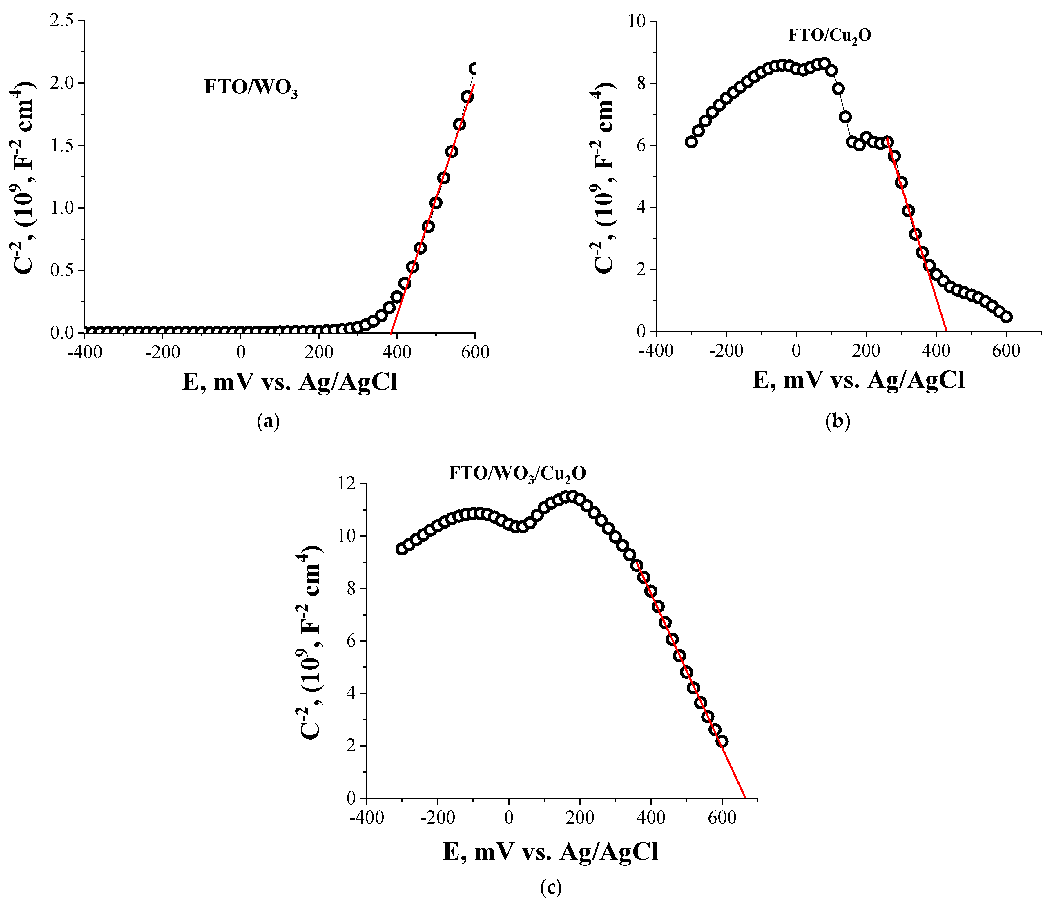
3.2. Electrochemical Characterization

Figure 3 demonstrates Mott–Schottky plots for FTO/WO3 (a), FTO/Cu2O (b) individual component electrodes, and the FTO/WO3/Cu2O heterostructured electrode. The positive slope in the Mott–Schottky plot for WO3 indicates the n-type conductivity of the SC, while, accordingly, the negative slope observed for the Cu2O Mott–Schottky plot corresponds to the p-type conductivity. The flat band potential of the electrodes was evaluated by extrapolating the Mott–Schottky plot slope to the X-axis. The corresponding values of the flat band potentials are 387 mV (vs. Ag/AgCl) for FTO/WO3 and 427 mV (vs. Ag/AgCl) for FTO/Cu2O electrodes.
The Mott–Schottky plot for the Cu2O electrode also demonstrates several characteristic peaks (Figure 3) at specific potential values, which are also observed in the cyclic voltametric (CV) dependences of the electrode (Figure S7a). These reversible characteristic peak CV dependencies can be attributed to the transitions Cu+ ↔ Cu2+ (~+200 mV vs. Ag/AgCl) and to the formation of Cu0 states (~−250 mV vs. Ag/AgCl), which indicates an electrochemical instability of the electrode material. Similar redox transitions were reported in [22]. The CV dependence for WO3 is typical for electrochemically stable semiconductors (Figure S5b).
Heterostructured FTO/WO3/Cu2O electrodes demonstrate p-type conductivity behavior. Therefore, one can infer that heterostructured electrode behavior is dictated mainly by the Cu2O outer layer in heterostructures. However, it is wise to note that within the potential range 0–200 mV (vs. Ag/AgCl), a switching in conductivity type from p-type to n-type is observed. This switching can indicate a possible realization of the different regimes of charge transfer through heterojunctions.
Remarkably, the flat band potential value of the heterostructured electrode is shifted toward a more positive potential by 240 mV compared to the flat band potential of the individual Cu2O electrode. These shifts correspond to the decrease in the energy positions of the top of the valence bands for the heterostructured electrode compared to the Cu2O electrode (see Table 1). Thus, one can conclude that the alteration of the flat band potentials of the heterostructured electrode is induced by the successful formation of a heterojunction between Cu2O and WO3.

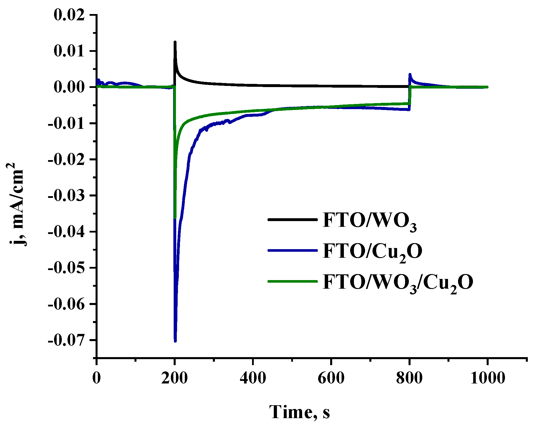
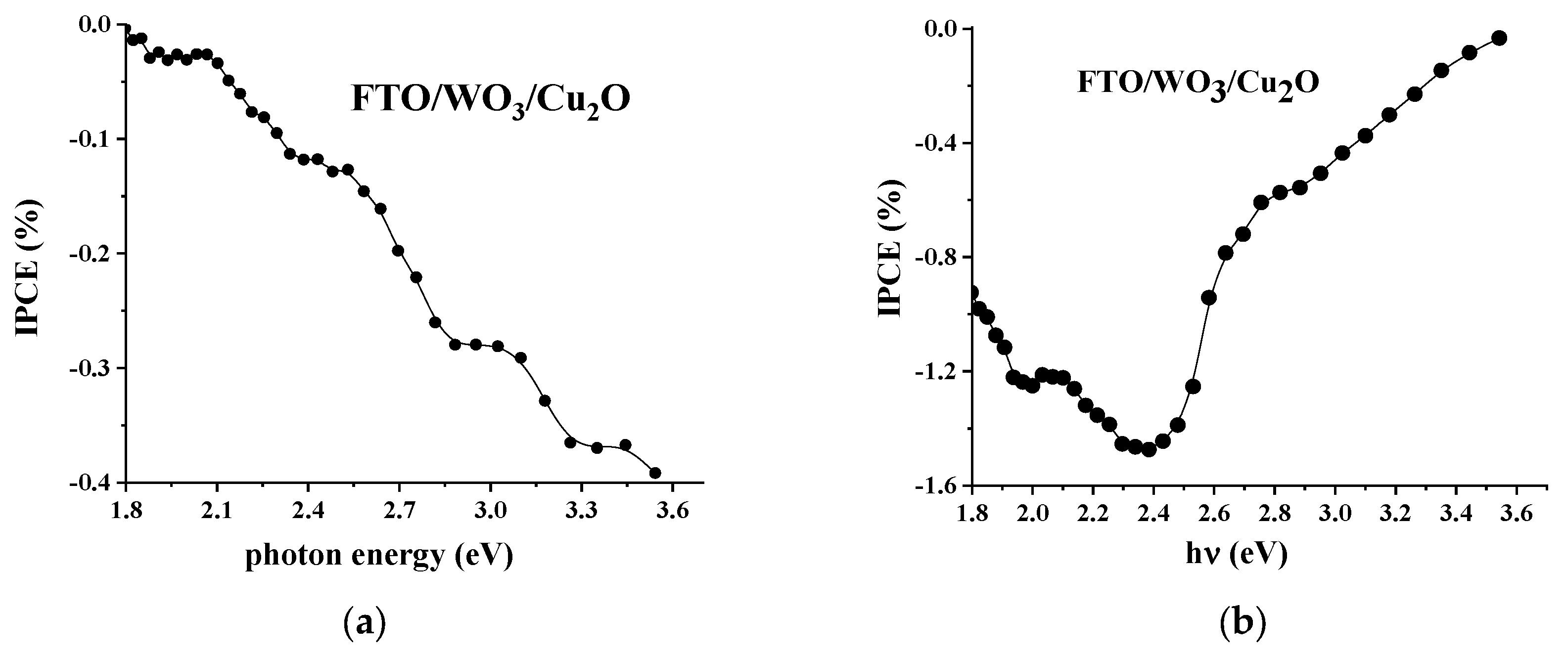
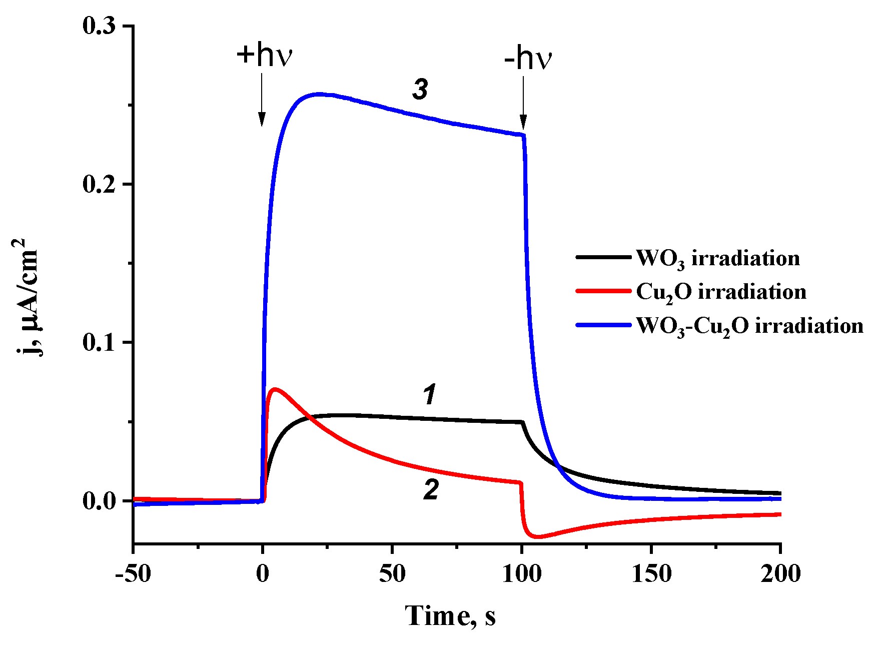
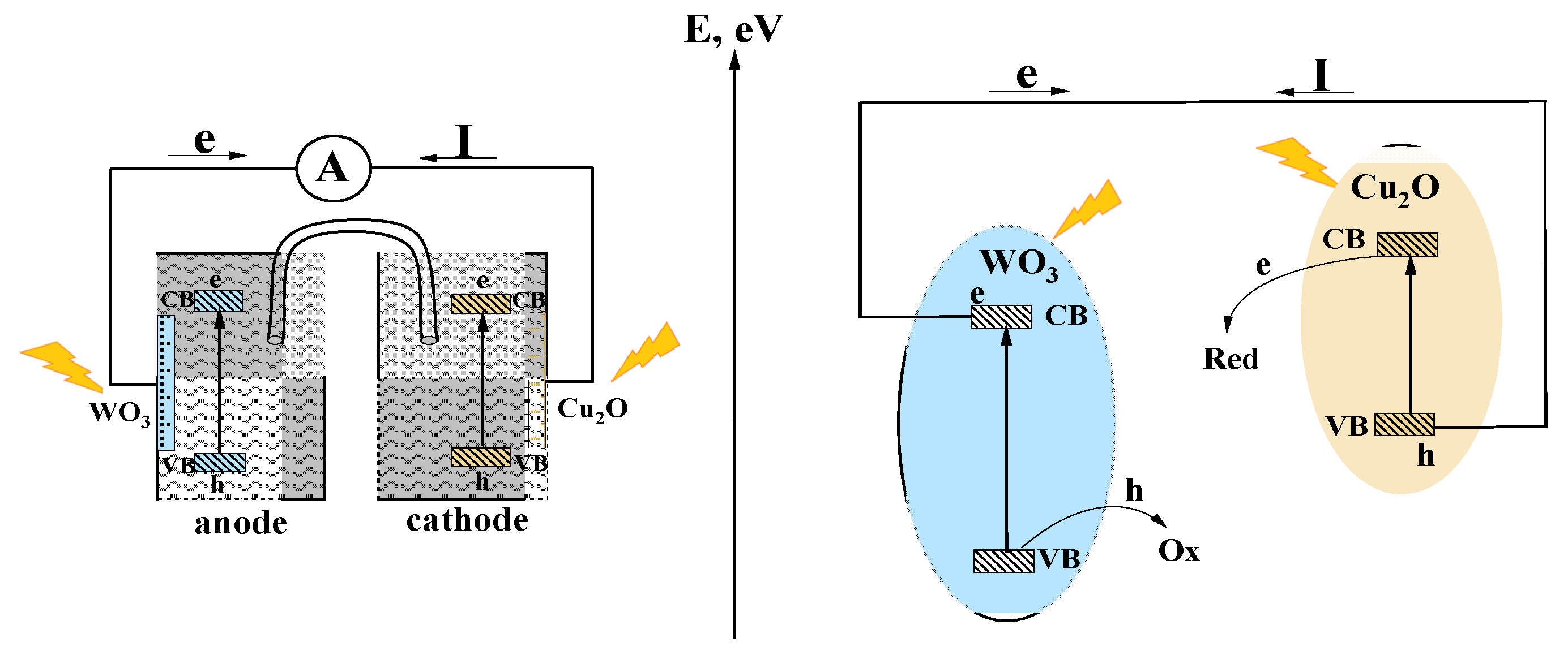
3.3. Photoelectrochemical Studies

To clarify the mechanism of charge separation and transfer in the heterostructured FTO/WO3/Cu2O electrode, we explored the photocurrent behavior (anodic current vs. cathodic current) and spectral dependences of incident photon-to-current conversion efficiencies (IPCEs), which is defined as:
I P C E ( % ) = 1239.8 j p h I m c h r λ × 100 %
where 1239.8 (V nm) is a multiplication of Plank’s constant, h, and the speed of light, c; jph (mA cm−2) is the stationary photocurrent density that was taken from chronoamperometry measurements; Imchr (mW cm−2) is the power density of acting monochromatic light; and λ (nm) is the wavelength of this monochromatic light. Also, we explored the photocurrent characteristics in the tandem PEC, where WO3 acts as the photoanode and Cu2O performs as the photocathode.
Figure 4 demonstrates the chronoamperometric dependences of the photocurrent for the FTO/WO3, FTO/Cu2O, and FTO/WO3/Cu2O electrodes under visible light irradiation without external bias.
As expected, the WO3 electrode demonstrates typical anodic behavior (positive photocurrent), while the Cu2O electrode acts as a typical photocathode (negative photocurrent) under visible light photoexcitation. It is wise to note that the cathodic photocurrent generated by the photoexcitation of the Cu2O electrode is significantly larger (about 35 times) than the anodic photocurrent induced by the irradiation of the WO3 electrode. Thus, one can conclude that WO3 properties could be a limiting factor for photoelectrochemical behavior in both the heterostructured WO3/Cu2O electrode and the tandem WO3||Cu2O PEC.
Remarkably, under broad irradiation with visible light, the heterostructured WO3/Cu2O electrode also demonstrates cathodic behavior typical for Cu2O forming the outer layer of the heterostructure. Moreover, the photocurrent generated by the heterostructured electrode is practically the same as the photocurrent generated by the individual Cu2O electrode. This infers that charge separation at the heterojunction significantly suppresses the recombination charge carrier losses in WO3, which is, apparently, a major factor for the lower activity of the individual WO3 electrode.
Figure S8 and Figure 5 demonstrate IPCE spectral dependencies measured for the single-component electrodes and for the heterostructured electrode, respectively.
Spectral dependences of the single-component electrodes (Figure S8), WO3 and Cu2O, demonstrate typical behavior with maximal efficiency, corresponding to the fundamental absorption of the corresponding photoactive materials, and confirm the anodic and cathodic characteristics for WO3 and Cu2O, respectively, in the whole spectral range. Remarkably, WO3 demonstrates minor activity in the extrinsic absorption spectral region, likely due to the excitation of defect states.
The analysis of the IPCE spectral dependencies obtained for the heterostructured electrode demonstrates several remarkable features of the photoelectrochemical behavior: first, the WO3/Cu2O heterostructured electrode behaves as a photocathode within the whole spectral range of photoexcitation. Taking into consideration that the spatial structure of the WO3/Cu2O electrode is planar, this infers that the major pathway of charge separation and transfer at the heterojunction is a realization of the Z-scheme mechanism. The Z-scheme is the only way to observe cathodic photoelectrochemical behavior (cathodic photocurrent) for the WO3/Cu2O heterostructured electrode since charge separation at the conventional type II heterojunction should result in anodic behavior. Second, unlike Cu2O, in which reliable photoactivity starts from the photon energy corresponding to the band gap value (2.4–2.5 eV) and, therefore, reflects the initiation of the band-to-band electronic transitions in Cu2O, the photoactivity of the heterostructured electrode is observed at significantly lower photon energies. Specifically, this is brightly demonstrated in the case of the back-side irradiation of the heterostructured electrode (from the WO3 layer side). The appearance of the significant photoactivity of the heterostructure within the photon energy range 1.8–2.4 eV can be explained by the photoexcitation of electronic states created at the heterojunction during the formation of the planar heterostructure. In turn, typically, these heterojunction electronic states can play the role of intermediates in heterojunction recombination and, therefore, promote the realization of the Z-scheme of charge separation when both WO3 and Cu2O components are photoexcited. Third, the observed spectral dependencies of IPCE strongly depend on the irradiation condition: the front side vs. the back side of the electrode. Indeed, front-side irradiation results in an increase in the cathodic efficiency of the heterostructured electrode with an increase in the energy of the actinic photons, while under irradiation from the back side of the electrode, the increase in photon energy leads to a decay in IPCE practically to zero at photon energies corresponding to the fundamental absorption of WO3. This behavior correlates with the transmittance spectrum of the heterostructure, where transmittance becomes nearly zero in the same spectral range. This observation indicates that in the case of back-side irradiation, all photons are absorbed within the inner WO3 layer of the heterostructure and cannot reach the heterojunction space and the outer Cu2O layer.
To confirm the realization of the Z-scheme in the WO3/Cu2O heterostructure, we explored the photoelectrochemical behavior of the tandem PEC with the WO3 electrode acting as the photoanode and the Cu2O electrode acting as the photocathode. Figure 6 demonstrates the chronoamperometric dependencies of the photocurrent in the tandem PEC for different irradiation conditions: photoexcitation of the anode only, photoexcitation of the cathode only, and photoexcitation of both electrodes.
As evident from the presented data (Figure 6), the photoexcitation of both electrodes results in a significant increase in the photocurrent compared to the photoexcitation of the individual electrodes. Moreover, the effect of photocurrent increase is not additive but rather synergetic.
According to the energy diagram (Figure 2), the tandem PEC can provide such a synergetic effect and stable anodic photocurrent only because of the realization of the mechanism of charge transfer in the tandem PEC matches the Z-scheme of charge separation and transfer, considering the external circuit as an intermediate interface playing the same role as the heterojunction in the heterostructure (Figure 7).
Thus, based on the presented results, we conclude that the major mechanism of charge separation and transfer in the WO3/Cu2O heterostructure and in the WO3||Cu2O tandem PEC is a Z-scheme realization.

4. Conclusions

Based on the presented results, we conclude that the major mechanism of charge separation and transfer in the WO3/Cu2O heterostructure and in the WO3||Cu2O tandem PEC is a Z-scheme realization. The photoelectrochemical efficiency of the heterostructured electrode also strongly depends on the irradiation conditions, i.e., the wavelength of photoexcitation and the direction of irradiation, either from the front side or from the back side. Irradiation from the back side is strongly blocked by WO3 light absorption. Therefore, the realization of the tandem PEC is more favorable from a practical point of view. An essential role in the expansion of the spectral range of the active photoexcitation might be ascribed to the interfacial electronic states at the heterojunction. They also can promote an effective realization of the Z-scheme mechanism.

Supplementary Materials

The following supporting information can be downloaded at https://www.mdpi.com/article/10.3390/nano14242057/s1: Figure S1: SEM images of the surface of the studied electrodes; Figure S2: X-ray diffraction patterns of the individual WO3 and Cu2O and heterostructured WO3/Cu2O electrodes; Figure S3: XPS survey spectra for the WO3 (black line), Cu2O (red line), FTO/WO3/Cu2O (blue line) electrodes; Figure S4: XPS high-resolution spectra of recorded for Cu2p states in FTO/Cu2O, FTO/WO3/Cu2O electrodes, O1S for FTO/WO3, FTO/Cu2O, FTO/WO3/Cu2O electrodes, and W 4f for the FTO/WO3 electrode; Figure S5: UPS spectra of the WO3, Cu2O, and FTO/WO3/Cu2O electrodes (UV monochromatic light source—HeI (21.22 eV)); Figure S6: Transmission spectra and Tauc plots for the Cu2O, WO3, and heterostructured WO3/Cu2O electrodes; Figure S7: CV curves of individual and heterostructured electrodes; Figure S8: Spectral dependence of the photocurrent for the WO3 and Cu2O electrodes.

Author Contributions

Conceptualization, A.V.E.; methodology, A.A.M., A.V.R., and A.V.E.; software, A.A.M. and T.V.B.; validation, A.A.M., A.V.R., and T.V.B.; formal analysis, A.A.M. and T.V.B.; investigation, A.A.M., T.V.B., and A.V.R.; resources, A.V.E.; data curation, A.A.M. and T.V.B.; writing—original draft preparation, A.A.M. and A.V.R.; writing—review and editing, A.V.E.; visualization, A.A.M. and A.V.R.; supervision, A.V.E.; project administration, D.W.B.; funding acquisition, A.V.E. and D.W.B. All authors have read and agreed to the published version of the manuscript.

Funding

This research was supported by the Russian Science Foundation (project No. 22-13-00155).

Data Availability Statement

The main data are provided in this article and the Supplementary Materials. Any other raw/processed data required to reproduce the findings of this study are available from the corresponding author upon request.

Acknowledgments

Authors are thankful to the “Centre for X-ray Diffraction Studies”, “Centre for Physical Methods of Surface Investigation”, “Geomodel”, “Nanophotonics”, and “Nanotechnology” of the Research Park at Saint Petersburg State University for helpful assistance in the preparation and characterization of the samples. The electrophysical and electrochemical measurements were carried out in the laboratory “Photoactive nanocomposite materials” supported by Saint Petersburg State University (research project 121121000186-3).

Conflicts of Interest

The authors declare no conflicts of interest.

References

  1. Chen, S.; Takata, T.; Domen, K. Particulate photocatalysts for overall water splitting. Nat. Rev. Mater. 2017, 2, 17050. [Google Scholar] [CrossRef]
  2. Nishioka, S.; Osterloh, F.E.; Wang, X.; Mallouk, T.E.; Maeda, K. Photocatalytic water splitting. Nat. Rev. Methods Primers 2023, 3, 42. [Google Scholar] [CrossRef]
  3. Marschall, R. 50 years of materials research for photocatalytic water splitting. Eur. J. Inorg. Chem. 2021, 2021, 2435–2441. [Google Scholar] [CrossRef]
  4. Thompson, W.A.; Fernandez, E.S.; Maroto-Valer, M.M. Review and analysis of CO2 photoreduction kinetics. ACS Sustain. Chem. Eng. 2020, 8, 4677–4692. [Google Scholar] [CrossRef]
  5. Behera, A.; Kar, A.K.; Srivastava, R. Challenges and prospects in the selective photoreduction of CO2 to C1 and C2 products with nanostructured materials: A review. Mater. Horiz. 2022, 9, 607–639. [Google Scholar] [CrossRef]
  6. Wang, W.-N.; Soulis, J.; Yang, Y.J.; Biswas, P. Comparison of CO2 photoreduction systems: A Review. Aerosol Air Qual. Res. 2014, 14, 533–549. [Google Scholar] [CrossRef]
  7. Hisatomi, T.; Kubota, J.; Domen, K. Recent advances in semiconductors for photocatalytic and photoelectrochemical water splitting. Chem. Soc. Rev. 2014, 43, 7520–7535. [Google Scholar] [CrossRef]
  8. Yuan, L.; Xu, Y.-J. Photocatalytic conversion of CO2 into value-added and renewable fuels. Appl. Surf. Sci. 2015, 342, 154–167. [Google Scholar] [CrossRef]
  9. Chen, X.; Shen, S.; Guo, L.; Mao, S.S. Semiconductor-based photocatalytic hydrogen generation. Chem. Rev. 2010, 110, 6503–6570. [Google Scholar] [CrossRef]
  10. Fu, W.; Guan, X.; Wu, H.; Liu, M. Switching from two-electron to four-electron photocatalytic pure water splitting via band bending engineering with boosted activity. Appl. Catal. B 2022, 305, 121054. [Google Scholar] [CrossRef]
  11. Salazar-Marín, D.; Oza, G.; Díaz Real, J.A.; Cervantes-Uribe, A.; Pérez-Vidal, H.; Kesarla, M.K.; Torres, J.G.T.; Godavarthi, S. Distinguishing between type II and S-scheme heterojunction materials: A comprehensive review. Appl. Surf. Sci. Adv. 2024, 19, 100536. [Google Scholar] [CrossRef]
  12. Liao, G.; Li, C.; Li, X.; Fang, B. Emerging polymeric carbon nitride Z-scheme systems for photocatalysis. Cell Rep. Phys. Sci. 2021, 2, 100355. [Google Scholar] [CrossRef]
  13. Song, W.; Chong, K.C.; Qi, G.; Xiao, Y.; Chen, G.; Li, B.; Tang, Y.; Zhang, X.; Yao, Y.; Lin, Z.; et al. Unraveling the transformation from type-II to Z-scheme in perovskite-based heterostructures for enhanced photocatalytic CO2 reduction. J. Am. Chem. Soc. 2024, 146, 3303–3314. [Google Scholar] [CrossRef] [PubMed]
  14. Di Liberto, G.; Tosoni, S.; Pacchioni, G. Z-Scheme versus type-II junction in g-C3N4/TiO2 and g-C3N4/SrTiO3/TiO2 heterostructures. Catal. Sci. Technol. 2021, 11, 3589–3598. [Google Scholar] [CrossRef]
  15. Murashkina, A.A.; Bakiev, T.V.; Artemev, Y.M.; Rudakova, A.V.; Emeline, A.V.; Bahnemann, D.W. Photoelectrochemical behavior of the ternary heterostructured systems CdS/WO3/TiO2. Catalysts 2019, 9, 999. [Google Scholar] [CrossRef]
  16. Minggu, L.J.; Ng, K.H.; Kadir, H.A.; Kassim, M.B. Bilayer n-WO3/p-Cu2O photoelectrode with photocurrent enhancement in aqueous electrolyte photoelectrochemical reaction. Ceram. Int. 2014, 40, 16015–16021. [Google Scholar] [CrossRef]
  17. Khalifa, M.A.; Shen, L.; Zheng, J.; Xu, C. Boosting light harvesting and charge separation of WO3 via coupling with Cu2O/CuO towards highly efficient tandem photoanodes. RSC Adv. 2021, 11, 13513–13520. [Google Scholar] [CrossRef]
  18. Emeline, A.V.; Rudakova, A.V.; Ryabchuk, V.K.; Serpone, N. Recent advances in composite and heterostructured photoactive materials for the photochemical conversion of solar energy. Curr. Opin. Green Sustain. 2022, 34, 100588. [Google Scholar] [CrossRef]
  19. Li, L.; Li, J.; Kim, B.K.H.; Huang, J. The effect of morphology and crystal structure on the photocatalytic and photoelectrochemical performances of WO3. RSC Adv. 2024, 14, 2080–2087. [Google Scholar] [CrossRef]
  20. Shin, S.; Han, H.S.; Kim, J.S.; Park, I.J.; Lee, M.H.; Hong, K.S.; Cho, I.S. A tree-like nanoporous WO3 photoanode with enhanced charge transport efficiency for photoelectrochemical water oxidation. J. Mater. Chem. A 2015, 3, 12920–12926. [Google Scholar] [CrossRef]
  21. Su, Q.; Zuo, C.; Liu, M.; Tai, X. A review on Cu2O-based composites in photocatalysis: Synthesis, modification, and applications. Molecules 2023, 28, 5576. [Google Scholar] [CrossRef] [PubMed]
  22. Toe, C.Y.; Zheng, Z.; Wu, H.; Scott, J.; Amal, R.; Ng, W.H. Photocorrosion of cuprous oxide in hydrogen production: Rationalising self-oxidation or self-reduction. Angew. Chem. 2018, 57, 13613–13617. [Google Scholar] [CrossRef] [PubMed]
  23. Chen, S.; Wang, L.-W. Thermodynamic oxidation and reduction potentials of photocatalytic semiconductors in aqueous solution. Chem. Mater. 2012, 24, 3659–3666. [Google Scholar] [CrossRef]
  24. Knöppel, J.; Kormányos, A.; Mayerhöfer, B.; Hofer, A.; Bierling, M.; Bachmann, J.; Thiele, S.; Cherevko, S. Photocorrosion of WO3 photoanodes in different electrolytes. ACS Phys. Chem Au 2021, 1, 6–13. [Google Scholar] [CrossRef]
  25. Shandilya, P.; Sambyal, S.; Sharma, R.; Mandyal, P.; Fang, B. Properties, optimized morphologies, and advanced strategies for photocatalytic applications of WO3 based photocatalysts. J. Hazard. Mater. 2022, 428, 128218. [Google Scholar] [CrossRef]
  26. Li, J.; Guo, C.; Li, L.; Gu, Y.; BoK-Hee, K.; Huang, J. Construction of Z-scheme WO3-Cu2O nanorods array heterojunction for efficient photocatalytic degradation of methylene blue. Inorg. Chem. Commun. 2022, 138, 109248. [Google Scholar] [CrossRef]
  27. Mandyal, P.; Sharma, R.; Sambyal, S.; Islam, N.; Priye, A.; Kumar, M.; Chauhan, V.; Shandilya, P. Cu2O/WO3: A promising S-scheme heterojunction for photocatalyzed degradation of carbamazepine and reduction of nitrobenzene. J. Water Process Eng. 2024, 59, 105008. [Google Scholar] [CrossRef]
  28. Ali, H.; Guler, A.; Masar, M.; Urbanek, P.; Urbanek, M.; Skoda, D.; Suly, P.; Machovsky, M.; Galusek, D.; Kuritka, I. Solid-state synthesis of direct Z-scheme Cu2O/WO3 nanocomposites with enhanced visible-light photocatalytic performance. Catalysts 2021, 11, 293. [Google Scholar] [CrossRef]
  29. Fu, Y.; Yang, J.; Wang, J.; Cao, L. Effects of Cu2O thickness on the photoelectrochemical properties of Cu2O/WO3 heterostructure. Vacuum 2023, 207, 111680. [Google Scholar] [CrossRef]
  30. Hao, J.; Qi, B.; Wei, J.; Li, D.; Zeng, F. A Z-scheme Cu2O/WO3 heterojunction for production of renewable hydrocarbon fuel from carbon dioxide. Fuel 2021, 287, 119439. [Google Scholar] [CrossRef]
  31. Shi, W.; Guo, X.; Cui, C.; Jiang, K.; Li, Z.; Qu, L.; Wang, J.-C. Controllable synthesis of Cu2O decorated WO3 nanosheets with dominant (0 0 1) facets for photocatalytic CO2 reduction under visible-light irradiation. Appl. Catal. B 2019, 243, 236–242. [Google Scholar] [CrossRef]
  32. Hu, C.-C.; Nian, J.-N.; Teng, H. Electrodeposited p-type Cu2O as photocatalyst for H2 evolution from water reduction in the presence of WO3. Sol. Energy Mater. Sol. Cells 2008, 92, 1071–1076. [Google Scholar] [CrossRef]
  33. Zheng, G.; Wang, J.; Li, H.; Li, Y.; Hu, P. WO3/Cu2O heterojunction for the efficient photoelectrochemical property without external bias. Appl. Catal. B 2024, 265, 118561. [Google Scholar] [CrossRef]
  34. Zhang, J.; Ma, H.; Liu, Z. Highly efficient photocatalyst based on all oxides WO3/Cu2O heterojunction for photoelectrochemical water splitting. Appl. Catal. B 2017, 201, 84–91. [Google Scholar] [CrossRef]
  35. Lin, C.Y.; Lai, Y.H.; Mersch, D.; Reisner, E. Cu2O|NiOx nanocomposite as an inexpensive photocathode in photoelectrochemical water splitting. Chem. Sci. 2012, 3, 3482–3487. [Google Scholar] [CrossRef]
  36. Shi, W.; Wang, J.C.; Chen, A.; Xu, X.; Wang, S.; Li, R.; Zhang, W.; Hou, Y. Cu nanoparticles modified step-scheme Cu2O/WO3 heterojunction nanoflakes for visible-light-driven conversion of CO2 to CH4. Nanomaterials 2022, 12, 2284. [Google Scholar] [CrossRef]
  37. Wu, L.; Tsui, L.; Swami, N.; Zangari, G. Photoelectrochemical stability of electrodeposited Cu2O films. J. Phys. Chem. C 2010, 114, 11551–11556. [Google Scholar] [CrossRef]
  38. de Jongh, P.E.; Vanmaekelbergh, D.; Kelly, J.J. Photoelectrochemistry of electrodeposited Cu2O. J. Electrochem. Soc. 2000, 147, 486. [Google Scholar] [CrossRef]
  39. Li, X.; Kong, W.; Qin, X.; Qu, F.; Lu, L. Self-powered cathodic photoelectrochemical aptasensor based on in situ–synthesized CuO-Cu2O nanowire array for detecting prostate-specific antigen. Microchim. Acta 2020, 187, 325. [Google Scholar] [CrossRef]
  40. Tao, X.; Wu, Y.; Sha, H. Cuprous oxide-modified diatomite waste from the brewery used as an effective adsorbent for removal of organic dye: Adsorption performance, kinetics and mechanism studies. Water Air Soil Pollut. 2018, 229, 322. [Google Scholar] [CrossRef]
  41. Zeng, X.; Gao, Q.; Song, P.; Zhang, X.; Xie, J.; Dong, Q.; Qi, J.; Xing, X.S.; Du, J. Integration of a Cu2O/ZnO heterojunction and Ag@SiO2 into a photoanode for enhanced solar water oxidation. RSC Adv. 2024, 14, 4568–4574. [Google Scholar] [CrossRef] [PubMed]
  42. Yin, X.; Liu, Q.; Yang, Y.; Liu, Y.; Wang, K.; Li, Y.; Li, D.; Qiu, X.; Li, W.; Li, J. An efficient tandem photoelectrochemical cell composed of FeOOH/TiO2/BiVO4 and Cu2O for self-driven solar water splitting. Int. J. Hydrogen Energy 2019, 44, 594–604. [Google Scholar] [CrossRef]
  43. NIST X-ray Photoelectron Spectroscopy Database. Available online: https://srdata.nist.gov/xps/ (accessed on 19 December 2024).
  44. Tsarenko, A.; Gorshenkov, M.; Yatsenko, A.; Zhigunov, D.; Butova, V.; Kaichev, V.; Ulyankina, A. Electrochemical synthesis-dependent photoelectrochemical properties of tungsten oxide powders. ChemEngineering 2022, 6, 31. [Google Scholar] [CrossRef]
Figure 1. Energy diagram of the electronic band positions and possible charge transfer directions at the heterojunction in type II heterostructures.
Nanomaterials 14 02057 g001
Figure 2. Energy diagram for individual materials and the planar heterostructure WO3/Cu2O.
Nanomaterials 14 02057 g002
Figure 3. Mott–Schottky plots for FTO/WO3 (a), FTO/Cu2O (b) individual component electrodes, and the FTO/WO3/Cu2O (c) heterostructured electrode.
Nanomaterials 14 02057 g003
Figure 4. Chronoamperometric dependences of photocurrent density: FTO/WO3 (black), FTO/Cu2O (navy), and FTO/WO3/Cu2O (green), without external bias upon irradiation with λ > 410 nm.
Nanomaterials 14 02057 g004
Figure 5. IPCE spectral dependencies of the FTO/WO3/Cu2O heterostructured electrode under irradiation from the front side (a) and back side (b).
Nanomaterials 14 02057 g005
Figure 6. Chronoamperometric dependencies of photocurrent density in the tandem PEC for different irradiation conditions: photoexcitation of the WO3 anode only (1), photoexcitation of the Cu2O cathode only (2), and photoexcitation of both the WO3 and Cu2O electrodes (3).
Nanomaterials 14 02057 g006
Figure 7. Scheme of electron transfer in the tandem PEC and energy diagram of photogenerated charge transfer in the WO3||Cu2O tandem system.
Nanomaterials 14 02057 g007
Table 1. Positions of the conduction and valence bands and band gap energies of the heterostructure components with respect to the vacuum energy level.
ElectrodeEg, eVEVB, eVECB, eVEF, eV WF, eV
FTO/WO32.8−7.3−4.5−4.895.0 ± 0.1
FTO/Cu2O2.4−5.9−3.5−4.834.8 ± 0.1
FTO/WO3/Cu2O 2.5 (Cu2O)
2.8 (WO3)
−6.1−3.6−4.854.9 ± 0.1
Disclaimer/Publisher’s Note: The statements, opinions and data contained in all publications are solely those of the individual author(s) and contributor(s) and not of MDPI and/or the editor(s). MDPI and/or the editor(s) disclaim responsibility for any injury to people or property resulting from any ideas, methods, instructions or products referred to in the content.

