Abstract
Two-dimensional material indium selenide (InSe) holds great promise for applications in electronics and optoelectronics by virtue of its fascinating properties. However, most multilayer InSe-based transistors suffer from extrinsic scattering effects from interface disorders and the environment, which cause carrier mobility and density fluctuations and hinder their practical application. In this work, we employ the non-destructive method of van der Waals (vdW) integration to improve the electron mobility of back-gated multilayer InSe FETs. After introducing the hexagonal boron nitride (h-BN) as both an encapsulation layer and back-gate dielectric with the vdW interface, as well as graphene serving as a buffer contact layer, the electron mobilities of InSe FETs are substantially enhanced. The vdW-integrated devices exhibit a high electron mobility exceeding 103 cm2 V−1 s−1 and current on/off ratios of ~108 at room temperature. Meanwhile, the electron densities are found to exceed 1012 cm−2. In addition, the fabricated devices show an excellent stability with a negligible electrical degradation after storage in ambient conditions for one month. Electrical transport measurements on InSe FETs in different configurations suggest that a performance enhancement with vdW integration should arise from a sufficient screening effect on the interface impurities and an effective passivation of the air-sensitive surface.
1. Introduction
Two-dimensional semiconductors (2DSM) have been widely employed as field effect transistor (FET) channel materials due to their tunable energy band structures and excellent electronic properties [1,2]. With dangling-bond-free surfaces and atomically uniform thicknesses, they hold great promise for replacing conventional silicon-based devices to overcome the performance limitations caused by short channel effects. Moreover, the transport behaviors of 2DSM could be manipulated through creating van der Waals (vdW) heterostructures without strict lattice matching or processing compatibility [3,4,5]. Unlike bulk materials, the performances of 2DSM-based devices are controlled and determined by the surface and interface characteristics of the channel, which typically involve the semiconductor surface, 2DSM-metal contact, and 2DSM–dielectric interface [6,7,8]. First, the surface effect in a 2DSM transistor mainly stems from the interaction between the surface of the channel and active ingredients in air, resulting in the modification of fundamental properties for sensitive 2DSM [9]. Second, the non-ideal 2DSM-metal contact is one of the major performance-limiting factors for 2DSM transistors, which arises from the gap states and interface disorders induced by the lithography and deposition processes and leads to the Fermi-level pinning (FLP) effect at the contact interface [10,11]. Third, the 2DSM–dielectric interface, especially for conventional dielectrics such as SiO2 and Al2O3, is responsible for the lowered carrier mobility due to the charged surface states, impurities, and surface roughness [12]. So far, extensive efforts have been made to improve the channel properties and push the performance limit of transistors by using various strategies, including contact optimization [13,14], reduction of impurity scattering [15], dielectric engineering [16,17,18], atomic vacancy healing and so on [19,20].
2D indium selenide (InSe) is a highly promising material for future nanoelectronics in virtue of several unique characteristics, such as a small effective electron mass, good charge transport behavior, and extraordinary mechanical properties [21,22]. Recent studies have shown that thin InSe layers exhibit spontaneous surface oxidation upon exposure to ambient atmosphere, forming charged traps at the surface and remarkable current hysteresis in transistors [23,24]. To address the reliability issue, various encapsulation approaches have been explored and proven to be effective in suppressing the infiltration of moisture and oxygen [25]. On the other hand, the charge transport of InSe transistors is sensitive to the dielectric environment. It has been revealed that the electron mobility of InSe nanosheets can be greatly improved by modulating the types of dielectric materials due to the strong suppression of carrier scattering [26,27]. In particular, integrating 2DSM with different dielectrics via vdW interactions provides vast opportunities for probing the intrinsic properties of 2DSM by creating high-quality interfaces with a low interfacial state density [28,29]. Despite the rapid progress in boosting the carrier mobility of InSe channels, its surface and interface issues must still be effectively addressed to push the development of high-performance InSe FETs [30,31].
In this study, we aim to improve the charge carrier mobility of InSe transistors by a non-destructive vdW integration process. In this approach, a hybrid gate dielectric, composed of a hexagonal boron nitride (h-BN) layer and subjacent SiO2 layer, is used to engineer the 2DSM–dielectric interface, a graphene buffer layer serves as electrical contacts to the InSe channel, and a top h-BN encapsulation layer is integrated to isolate the InSe layer from ambient conditions and achieve the long-term stability of the devices. This strategy enables us to gain a high electron mobility of up to 1078 cm2 V−1 s−1 at room temperature and an on/off ratio of up to ~108, which is larger than that of transistors based on the bare SiO2 dielectric and hybrid gate dielectric of polymer and Al2O3. Moreover, optoelectronic measurements in the multilayer InSe transistors show an excellent photoresponse with a high photoresponsivity and external quantum efficiency (EQE).
2. Materials and Methods
2.1. Fabrication of Multilayer InSe Transistors
Bulk h-BN and graphene crystals were purchased from HQ graphene. Bulk InSe crystals were synthesized from melting In powders and Se powders in a sealed vacuum tube inside a furnace. The sealed tube was heated to 700 °C for 3 h and kept at 700 °C for 3 days. After that, it was cooled to 500 °C for 2 days, followed by natural cooling. The back-gated FETs were fabricated using a layer-by-layer dry transfer method in an argon-filled glove box (H2O < 1 ppm, O2 < 1 ppm). First, the h-BN crystals were mechanically exfoliated using blue tape onto the polydimethylsiloxane (PDMS) and then transferred onto an oxidized silicon wafer, which was pre-processed by ultraviolet-ozone cleaning for 5 min. The silicon wafer with h-BN flakes was annealed on a hot stage in the glove box at 400 °C for 3 h. Then, two few-layer graphene flakes were transferred onto two ends of the bottom h-BN to serve as the buffer layer. The h-BN/graphene heterostructure was also annealed in the glove box at 400 °C for 3 h to remove processing residues. After that, the target InSe flakes on PDMS were aligned on the h-BN/graphene heterostructure so that the edges of the InSe flakes overlapped with the graphene layer. The h-BN/graphene/InSe heterostructure was annealed at 180 °C for 5 min. Finally, a larger h-BN flake was selected to encapsulate the heterostructure, followed by another annealing at 180 °C for 5 min. The metal electrodes of Cr/Au (10/50 nm) were patterned using a copper grid as the shadow mask and prepared by standard electron-beam evaporation (ASB-EPI-C6, Syskey Technology Co., Ltd., Hsinchu, Taiwan). The fabricated devices were annealed in an Ar atmosphere at 180 °C for 30 min to optimize the contact condition.
For the FETs devices with PMMA/Al2O3 bilayer dielectric, the 30 nm thick Al2O3 was grown by atomic layer deposition (ALD) System MNT-S100-L3S1 (MNT Micro and Nanotech Co., Ltd., Wuxi, China). The upper PMMA layer was fabricated by spin-coating (2000 rpm, 2 min) 2.5 wt% 950k PMMA on Al2O3/Si substrate and baked at 170 °C for 30 min.
2.2. Characterization and Device Measurement
The topographies and thicknesses of exfoliated nanosheets (InSe, graphene, h-BN) and films of PMMA and Al2O3 were identified by an optical microscope (Nikon Y-IDP) and AFM (Dimension ICON system, Bruker, Billerica, MA, USA). Raman and PL spectra of InSe nanosheets were collected by using a WITec Alpha 300R (Oxford Instruments, Abingdon, UK) confocal microscope spectrometer with an excitation laser of 532 nm. TEM sample was prepared by using the focused ion beam (FIB) system (FEI, Scios, Hopewell Township, NJ, USA). To protect the selected region from ion damage, a layer of 500 nm Pt and another layer of 2 μm Pt were successively deposited on the h-BN/InSe/h-BN heterostructure before FIB milling. The prepared cross-sectional slice was then transferred and attached to a TEM grid. TEM and EDS mapping images were performed on a JEOL JEM-3200FS operated at an accelerating voltage of 300 kV and equipped with an EDS detector.
The electrical properties of the InSe devices were measured in a probe station (Lakeshore, TTPX, Thebarton, Australia) in vacuum, using a Keithley (4200-SCS, Cleveland, OH, USA) semiconductor parameter analyzer. Photo-response was triggered by a supercontinuum white-light laser source (SC400-8, Fianium Ltd., Southampton, UK) coupled with a monochromator. The laser intensity was measured with a commercial Thorlabs power meter.
3. Results and Discussion
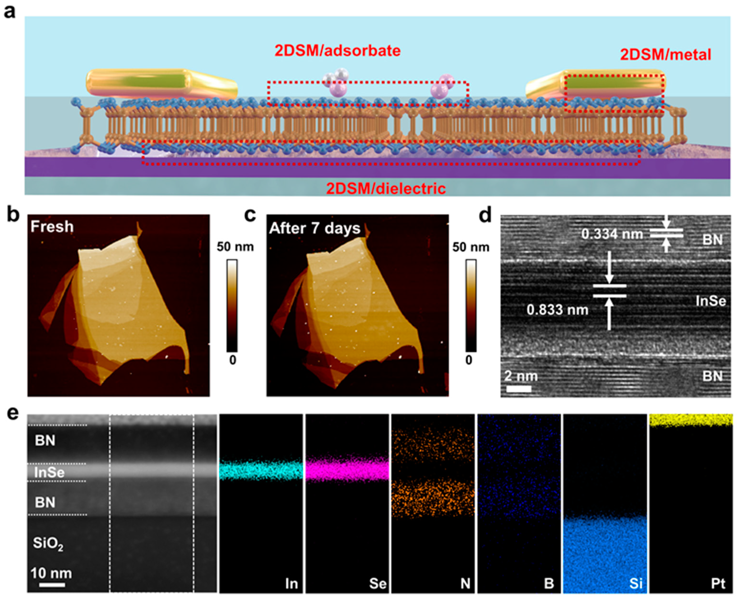
As illustrated in Figure 1a, there are three types of interfaces involved in the InSe FET device, including the InSe/adsorbate interface, InSe/metal contact, and InSe/dielectric interface. Figure 1b shows the atomic force microscopy (AFM) image of a 20 nm thick InSe nanosheet shortly after exfoliation, showing a uniform topography. After seven days of ambient exposure, the inspection of increased small protrusions on the surface suggested structural or chemical changes in the InSe nanosheet arising from the slow but spontaneous oxidation (Figure 1c) [23]. Moreover, the photoluminescent (PL) emission showed an appreciable reduction in intensity (Figure S1). Accordingly, the vdW integration method was employed to achieve pure van der Waal contacts and minimize defects and charge trapping sites by providing a high interface quality for optoelectronic devices [32]. In the realm of vdW integration, artificial heterostructures composed of 2DSM, graphene, and h-BN have gained extensive attention [28,33]. For the sake of simplicity, we fabricated vdW heterostructures composed of a multilayer InSe layer interlaid between thin h-BN layers using a dry alignment transfer procedure shown in Figure S2. High-resolution transmission electron microscopy (HRTEM) for the interface region was used to characterize the vdW interface region (Figure 1d). Obviously, the h-BN/InSe/h-BN stacking could produce damage-free and atomically smooth interfaces between disparate materials. The interlayer spacing was measured to be 0.334 nm and 0.833 nm, equal to the interlayer distance in h-BN and InSe, respectively. The corresponding energy-dispersive X-ray spectroscopy (EDS) element mappings in Figure 1e distinctly presented the individual components of the h-BN/InSe/h-BN heterostructure, including the deposited Pt layer, InSe layer, and top and bottom h-BN layers.

Figure 1.
(a) Schematic of the three types of interfaces in the InSe FET device, including InSe/adsorbate, InSe/metal contact, and InSe/dielectric interfaces, as highlighted by the dotted boxes. (b) AFM image of a fresh InSe nanosheet prepared by mechanical cleavage. (c) AFM image of the InSe nanosheet after seven days of ambient exposure. (d) Cross-sectional HRTEM image of h-BN/InSe/h-BN vdW heterostructure, showing good interface quality. (e) EDS element mappings of the h-BN/InSe/h-BN heterostructure.
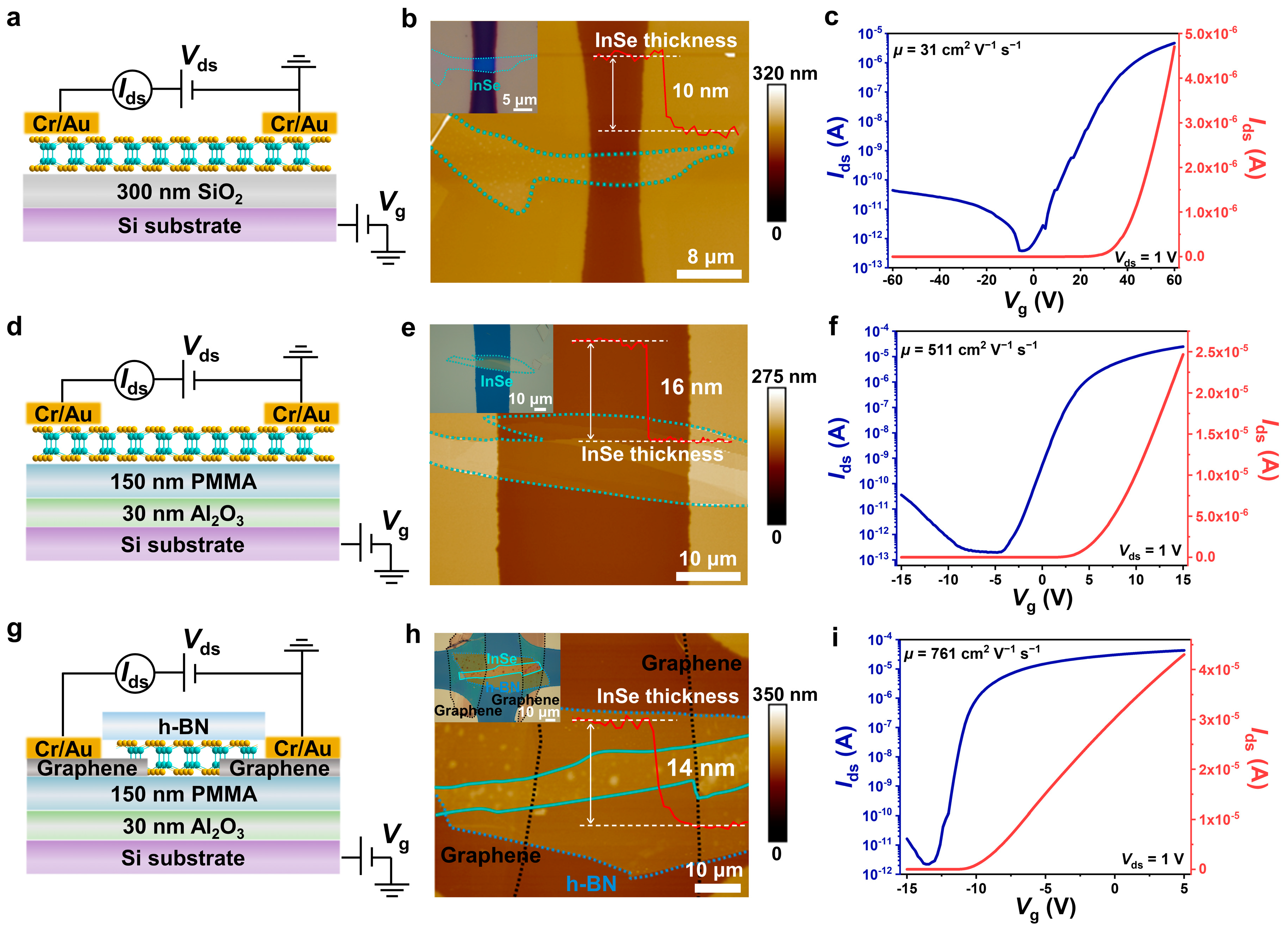
Apart from the surface structure, the interface between the InSe and dielectric layer is one of the crucial factors dominating the FET device performance. To this end, we fabricated different types of back-gated field effect transistor (FET) devices based on various dielectric layers using the home-made copper grid mask method. The InSe nanosheets with a thickness range of 10–30 nm were exfoliated from bulk crystals and transferred to silicon substrates. Figure 2a illustrates the schematic view of the InSe/SiO2 FET device based on a single 300 nm thick SiO2 dielectric. The thickness of the InSe channel was 10 nm, as measured by AFM in Figure 2b. The transfer and output characteristics of InSe/SiO2 FET were carried out by applying a drain-source voltage (Vds) and gate voltage (Vg) in a three-terminal configuration. Figure 2c presents the Ids-Vg curves of the typical InSe/SiO2 FET operated at Vds = 1 V, indicating an obvious n-type behavior with a current on/off ratio of 1.3 × 10⁷. The field-effect mobility can be extracted using the equation as follows:
where L and W are the channel length and width of the device; and Ci is the capacitance between the channel and the back gate per unit area: Ci = ε0εr/d, where ε0 = 8.85 × 10⁻¹² F m−1 and εr (3.9) and d (300 nm) are the dielectric constant and thickness of SiO2, respectively. Based on the transport curve, the electron mobility was calculated to be 31 cm2 V−1 s−1. The carrier scattering originating from the amorphous gate dielectric of SiO2 was primarily responsible for the low electron mobility [27,28]. The output curves of the InSe/SiO2 FET showed that a larger positive gate voltage induced a higher current due to the n-type conduction (Figure S3). To screen the interfacial Coulomb impurities, we also fabricated an InSe FET device based on a hybrid dielectric interface, composed of 150 nm poly(methyl methacrylate) (PMMA) and 30 nm Al2O3 (Figure 2d). The optical micrograph and AFM images of InSe/PMMA/Al2O3 FET are shown in Figure 2e. Figure 2f presents the Ids-Vg curves of the typical InSe/PMMA/Al2O3 device, demonstrating an electron mobility of 511 cm2 V−1 s−1 and on/off ratio of ~108, respectively. The carrier mobility was one order of magnitude higher than that from the FET device on the SiO2/Si substrate. Furthermore, multilayer InSe was encapsulated with h-BN to prevent absorbed impurities and oxidations on the channel surface. Figure 2g illustrates the schematic view of the h-BN/InSe/PMMA/Al2O3 FET device, with graphene serving as the buffer layer. The thickness of the InSe channel was identified to be 14 nm according to the AFM in Figure 2h. The mobility of h-BN/InSe/PMMA/Al2O3 FET was further enhanced to be 761 cm2 V−1 s−1 with an on/off ratio of 2.1 × 10⁷ (Figure 2i).
μ = (dIds/dVg) × L/(WCiVds)
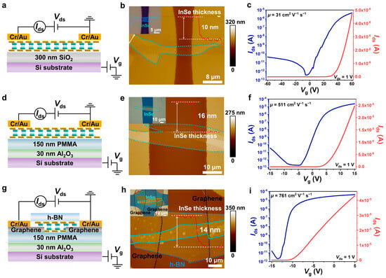
Figure 2.
(a,b) Schematic view and AFM image of the InSe FET based on bare SiO2 dielectric. Inset shows the corresponding optical image of the device. (c) Transfer characteristics of the device at Vds = 1 V at linear (red line) and logarithmic (blue line) scales. (d,e) Schematic view and AFM image of the InSe FET based on PMMA/Al2O3 dielectric without encapsulation. (f) Transfer characteristics of the device at Vds = 1 V at linear (red line) and logarithmic (blue line) scales. (g,h) Schematic view and AFM image of the h-BN-encapsulated InSe FET based on PMMA/Al2O3 dielectric. (i) Transfer characteristics of the device at Vds = 1 V at linear (red line) and logarithmic (blue line) scales.
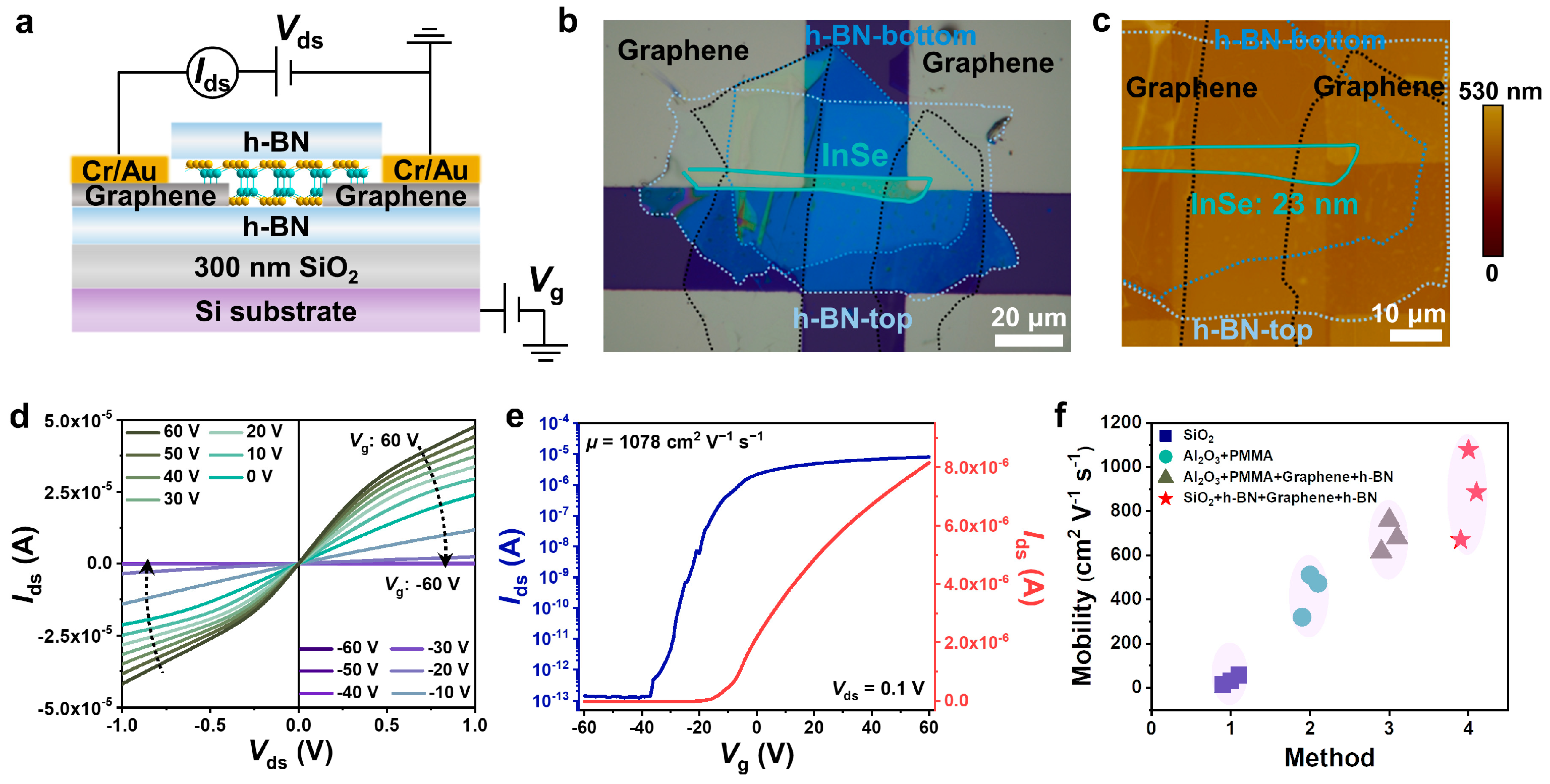
Recently, h-BN has been widely explored to optimize interface properties and electrical performance because of its high single crystallinity and vdW surfaces. A root-mean-square surface roughness of 0.19 nm was measured for the cleaved h-BN (Figure S4), which was almost the same as for the defect-free polymer of PMMA (0.29 nm). Hence, h-BN was further employed as both a gate dielectric and passivation layer to fabricate InSe FET devices using the vdW integration process. In addition, graphene nanosheets were used as a buffer layer to create a high-quality electrical contact and alleviate the damage of the InSe channel during the metal deposition process [34]. Details of the device fabrication process were described in the Materials and Methods section and Figure S5. Figure 3a,b display the schematic view of h-BN/InSe/h-BN/SiO2 FET and optical images of a typical device, respectively. The thickness of the InSe channel was determined to be 23 nm by AFM measurement (Figure 3c and Figure S6). Note that the channel was fully covered by a top h-BN layer, as marked by the light blue dotted line. Figure 3d shows the Ids-Vds curves for back gate voltages ranging from −60 to +60 V, indicating the good contact between the Cr/Au electrodes and InSe channel. The satisfactory performance should be attributed to the formation of a vdW contact with the insertion of an atomically flat graphene layer, which is efficient in preventing metal diffusion from electrodes to the channel and eliminating the metal-induced gap state [10]. Accordingly, the FLP effect between the InSe and Au electrode was alleviated, and an enhanced carrier mobility could be expected. Figure 3e shows the transfer curves of the h-BN/InSe/h-BN/SiO2 FET, resulting in a high electron mobility of 1078 cm2 V−1 s−1 and an on/off ratio of 7.1 × 10⁷ at room temperature. This mobility value was equivalent to the previous results from the top- or bottom-gated FET devices reported for multilayer InSe, which were optimized by interface engineering methods, including encapsulation, modifying the contact metal or dielectric layer, and surface charge doping [21,28,30]. The hysteresis behavior in the vdW-integrated InSe was also revealed. As shown in Figure S7, the device exhibited a diminutive hysteresis loop due to the decrease of interfacial trap densities, consistent with a previous study [12]. The carrier density (n) was calculated to be 2.5 × 1012 cm−2 according to the following equation [35], where q is the elemental charge:
n = (IdsL)/(qWVdsμ)
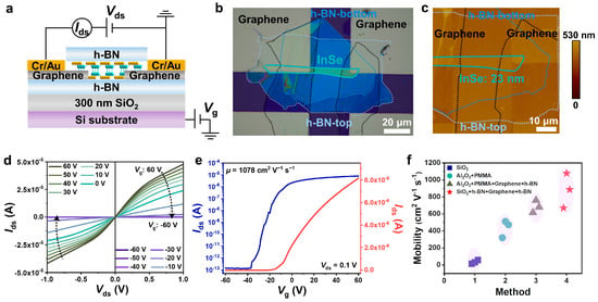
Figure 3.
(a) Schematic view of the h-BN-encapsulated InSe FET based on h-BN/SiO2 dielectric. (b,c) Optical image and the corresponding AFM image of the vdW-integrated h-BN/InSe/h-BN/SiO2 FET device. (d) Output characteristics of the device at different Vg. (e) Transfer characteristics of the device at Vds = 0.1 V at linear (red line) and logarithmic (blue line) scales. (f) The distribution of electron mobility for InSe devices with different configurations.
Moreover, Figure 3f and Figure S8 summarized the distribution of electron mobility (μ) for four types of multilayer InSe FET devices fabricated in different batches, as marked by square, circle, triangle, and star, respectively. Overall, the vdW-integrated InSe FETs exhibited a substantial improvement in carrier mobility compared to the case involving an InSe channel placed directly on the SiO2/Si substrate and also devices without encapsulation. Furthermore, the mobility of vdW-integrated devices was competitive with that of devices based on a PMMA dielectric layer, suggesting the effective screening of carrier scattering by h-BN. In order to see environmental stability, the evolution of the electrical properties of the devices was further measured. It turned out that the vdW-integrated devices could maintain a stable carrier mobility and current on/off ratio when they were stored under ambient conditions for one month (Figure S9). These experimental results indicate that the clean interface of the 2DSM/dielectric and the h-BN-passivated surface of the 2DSM channel contribute to the preservation of charge transport.
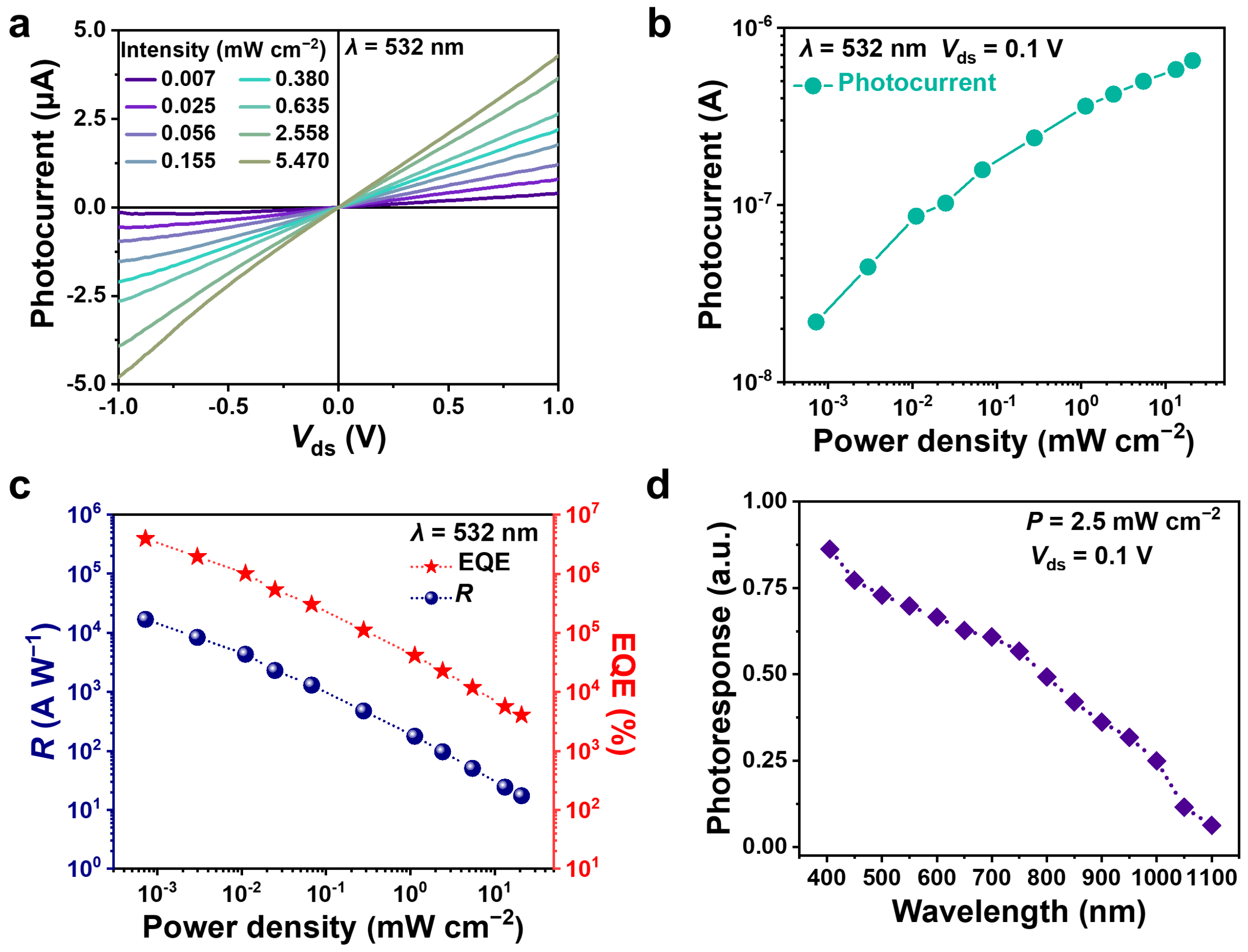
Furthermore, the photoresponse performance of the vdW-integrated InSe transistors was investigated. Under illumination of a 532 nm laser, the InSe device showed linear source-drain current-voltage (Ids − Vds) curves (Figure S10), indicating good electrical contact between the channel and metal electrodes. Furthermore, the photocurrent (Iph), defined as the difference between the device current measured under laser light illumination (Ilight) and that measured in the dark (Idark), increased monotonically when increasing the laser power density (P) of the incident laser light, as displayed in Figure 4a,b. To evaluate the photodetector performance, the photoresponsivity (R) and external quantum efficiency (EQE) were calculated according to the following equations:
where S is the effective area of the device, h is the Planck constant, and c is the speed of light. Figure 4c plots the value of photoresponsivity under different power densities. When the photodetector operated at Vds = 0.1 V and Vg = 0 V, a maximum photoresponsivity of 1.7 × 10⁴ A W−1 was obtained at a low power density of 7.2 × 10⁻⁴ mW cm−2. Meanwhile, EQE showed a similar trend to photoresponsivity when the power densities increased, resulting in a maximum value of 3.9 × 10⁶% at P = 7.2 × 10⁻⁴ mW cm−2. Figure 4d shows the wavelength-dependent photoresponsivity of the InSe device measured at a fixed laser power density of 2.5 mW cm−2 (Vds = 0.1 V, Vg = 0 V). When the photo energy was larger than the band gap (1.26 eV) of multilayer InSe, abundant electron–hole pairs would be excited and subsequently separated by the bias voltage, leading to an efficient photoresponse in the wavelength range of 400–950 nm. When the wavelength increased towards 1100 nm, the devices exhibited an obvious decrease in photoresponsivity due to the forbidden interband absorption, in agreement with a previous study [36].
R = Iph/(PS)
EQE = R/(hc/eλ)
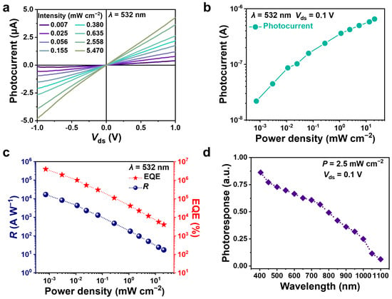
Figure 4.
(a) Iph − Vds curves of the vdW-integrated InSe device under different 532 nm laser power densities. (b) Dependence of the photocurrent on the power density at Vds = 0.1 V. (c) Dependence of the photoresponsivity and EQE on the power density. (d) Wavelength-dependent photoresponsivity under incident light illumination with a fixed power density of 2.5 mW cm−2.
4. Conclusions
In summary, we have demonstrated the drastic effect of interfacial and surface properties on the electrical properties of multilayer InSe by fabricating FET devices with different configurations. Taking advantage of the vdW integration technique, the h-BN/InSe/h-BN/SiO2 FET displayed room-temperature electron mobility exceeding 103 cm2 V−1 s−1 with an on/off ratio of 7.1 × 10⁷ and electron density of 2.5 × 1012 cm−2, respectively, which was an order of magnitude larger than that from FETs based on an oxide dielectric. Such an enhanced device performance was mainly due to a clean InSe/dielectric interface and vdW contact between the InSe channel and metal electrodes with the insertion of a graphene buffer layer. Moreover, the passivated surface of the InSe channel enabled an excellent environmental stability of the transistors. This work demonstrates that vdW integration of 2DSM is promising for realizing high-performance electronic devices.
Supplementary Materials
The following supporting information can be downloaded at: https://www.mdpi.com/article/10.3390/nano14040382/s1, Figure S1. Evolution of PL spectra for the exfoliated InSe nanosheet after seven days of ambient exposure. Figure S2. Optical image of the fabricated h-BN/InSe/h-BN heterostructure for characterization of the vdW interface. Figure S3. Output characteristics of (a) InSe/SiO2 FET, (b) InSe/PMMA/Al2O3 FET, and (c) h-BN/InSe/PMMA/Al2O3 FET devices at different Vg. Figure S4. 3D surface images of the cleaved h-BN and spin-coated PMMA film, with a root-mean-square surface roughness of 0.19 and 0.29 nm, respectively. Figure S5. Dry transfer process to fabricate a h-BN/InSe/h-BN/SiO2 vdW heterostructure with graphene as the buffer layer. Scale bars, 20 μm. Figure S6. Height profile extracted from InSe layer of the vdW-integrated heterostructure, showing a channel thickness of 23 nm. Figure S7. Transfer curves of the vdW-integrated FET with forward and backward scans of the gate voltages. Figure S8. Transfer characteristics at linear scales of (a) InSe/SiO2 FET, (b) InSe/330 nm PMMA/30 nm Al2O3 FET, (c) h-BN/InSe/150 nm PMMA/30 nm Al2O3 (up) and h-BN/InSe/330 nm PMMA/30 nm Al2O3 (bottom) FET, and (d) h-BN/InSe/h-BN/SiO2 FET devices, respectively. Figure S9. Comparison of transfer curves of the vdW-integrated FET after one month exposure to ambient atmosphere, revealing the excellent stability of the device. Figure S10. Ids − Vds curves of the vdW-integrated InSe device under dark conditions and different 532 nm laser power densities.
Author Contributions
Methodology, Z.L., J.L, H.O., Y.H., J.Z., J.H., H.L. and Y.T.; writing—original draft preparation, Q.H.; writing—review and editing, Z.L., J.L. and Q.H.; supervision, W.Z.; project administration, D.Q., Q.H. and W.Z.; funding acquisition, D.Q., Q.H. and W.Z. All authors have read and agreed to the published version of the manuscript.
Funding
This research was funded by the Science, Technology and Innovation Commission of Shenzhen Municipality (Grant No. JCYJ20200109105422876), the National Natural Science Foundation of China (NSFC)-Research Grant Council of Hong Kong (RGC) Key International (Regional) Joint Research Program (NSFC Grant No. 62261160574), the Guangdong Basic and Applied Basic Research Foundation (Grant No. 2022A1515110707), the National Natural Science Foundation of China (Grant No. 62104152), and the National Postdoctoral Research Fellowship Program (GZB20230450).
Data Availability Statement
Data are contained within the article and the Supplementary Material.
Conflicts of Interest
The authors declare no conflict of interest.
References
- Chhowalla, M.; Jena, D.; Zhang, H. Two-dimensional semiconductors for transistors. Nat. Rev. Mater. 2016, 1, 16052. [Google Scholar] [CrossRef]
- Wang, S.; Liu, X.; Xu, M.; Liu, L.; Yang, D.; Zhou, P. Two-dimensional devices and integration towards the silicon lines. Nat. Mater. 2022, 21, 1225–1239. [Google Scholar] [CrossRef]
- Liang, S.J.; Cheng, B.; Cui, X.; Miao, F. Van der Waals Heterostructures for High-Performance Device Applications: Challenges and Opportunities. Adv. Mater. 2019, 32, 1903800. [Google Scholar] [CrossRef] [PubMed]
- Liu, J.; Hao, Q.; Gan, H.; Li, P.; Li, B.; Tu, Y.; Zhu, J.; Qi, D.; Chai, Y.; Zhang, W.; et al. Selectively Modulated Photoresponse in Type-I Heterojunction for Ultrasensitive Self-Powered Photodetectors. Laser Photonics Rev. 2022, 16, 2200338. [Google Scholar] [CrossRef]
- Cen, Y.; Tu, Y.; Zhu, J.; Hu, Y.; Hao, Q.; Zhang, W. Photoinduced Contact Evolution and Junction Rearrangement in Two-Dimensional van der Waals Heterostructure. Adv. Funct. Mater. 2023, 33, 2306668. [Google Scholar] [CrossRef]
- Jiang, B.; Yang, Z.; Liu, X.; Liu, Y.; Liao, L. Interface engineering for two-dimensional semiconductor transistors. Nano Today 2019, 25, 122–134. [Google Scholar] [CrossRef]
- Hu, Z.; Wu, Z.; Han, C.; He, J.; Ni, Z.; Chen, W. Two-dimensional transition metal dichalcogenides: Interface and defect engineering. Chem. Soc. Rev. 2018, 47, 3100–3128. [Google Scholar] [CrossRef]
- John, J.W.; Mishra, A.; Debbarma, R.; Verzhbitskiy, I.; Goh, K.E.J. Probing charge traps at the 2D semiconductor/dielectric interface. Nanoscale 2023, 15, 16818–16835. [Google Scholar] [CrossRef]
- Jiang, B.; Huang, H.; Chen, R.; Li, G.; Flandre, D.; Wan, D.; Chen, X.; Liu, X.; Ye, C.; Liao, L. Black phosphorus field effect transistors stable in harsh conditions via surface engineering. Appl. Phys. Lett. 2020, 117, 111602. [Google Scholar] [CrossRef]
- Qi, D.; Li, P.; Ou, H.; Wu, D.; Lian, W.; Wang, Z.; Ouyang, F.; Chai, Y.; Zhang, W. Graphene-Enhanced Metal Transfer Printing for Strong van der Waals Contacts between 3D Metals and 2D Semiconductors. Adv. Funct. Mater. 2023, 33, 2301704. [Google Scholar] [CrossRef]
- Liu, X.; Choi, M.S.; Hwang, E.; Yoo, W.J.; Sun, J. Fermi Level Pinning Dependent 2D Semiconductor Devices: Challenges and Prospects. Adv. Mater. 2022, 34, 2108425. [Google Scholar] [CrossRef]
- Zhang, S.; Qiu, Y.; Yang, H.; Wang, D.; Hu, Y.; Lu, X.; Li, Z.; Hu, P. The role of hybrid dielectric interfaces in improving the performance of multilayer InSe transistors. J. Mater. Chem. C 2020, 8, 6701–6709. [Google Scholar] [CrossRef]
- Liu, Y.; Wu, H.; Cheng, H.-C.; Yang, S.; Zhu, E.; He, Q.; Ding, M.; Li, D.; Guo, J.; Weiss, N.O.; et al. Toward Barrier Free Contact to Molybdenum Disulfide Using Graphene Electrodes. Nano Lett. 2015, 15, 3030–3034. [Google Scholar] [CrossRef]
- Liu, Y.; Guo, J.; Zhu, E.; Liao, L.; Lee, S.-J.; Ding, M.; Shakir, I.; Gambin, V.; Huang, Y.; Duan, X. Approaching the Schottky–Mott limit in van der Waals metal–semiconductor junctions. Nature 2018, 557, 696–700. [Google Scholar] [CrossRef] [PubMed]
- Cui, X.; Lee, G.-H.; Kim, Y.D.; Arefe, G.; Huang, P.Y.; Lee, C.-H.; Chenet, D.A.; Zhang, X.; Wang, L.; Ye, F.; et al. Multi-terminal transport measurements of MoS2 using a van der Waals heterostructure device platform. Nat. Nanotechnol. 2015, 10, 534–540. [Google Scholar] [CrossRef] [PubMed]
- Cui, Y.; Xin, R.; Yu, Z.; Pan, Y.; Ong, Z.Y.; Wei, X.; Wang, J.; Nan, H.; Ni, Z.; Wu, Y.; et al. High-Performance Monolayer WS2 Field-Effect Transistors on High-κ Dielectrics. Adv. Mater. 2015, 27, 5230–5234. [Google Scholar] [CrossRef] [PubMed]
- Xu, Y.; Liu, T.; Liu, K.; Zhao, Y.; Liu, L.; Li, P.; Nie, A.; Liu, L.; Yu, J.; Feng, X.; et al. Scalable integration of hybrid high-κ dielectric materials on two-dimensional semiconductors. Nat. Mater. 2023, 22, 1078–1084. [Google Scholar] [CrossRef] [PubMed]
- Zhang, C.; Tu, T.; Wang, J.; Zhu, Y.; Tan, C.; Chen, L.; Wu, M.; Zhu, R.; Liu, Y.; Fu, H.; et al. Single-crystalline van der Waals layered dielectric with high dielectric constant. Nat. Mater. 2023, 22, 832–837. [Google Scholar] [CrossRef] [PubMed]
- Ahn, B.; Kim, Y.; Kim, M.; Yu, H.M.; Ahn, J.; Sim, E.; Ji, H.; Gul, H.Z.; Kim, K.S.; Ihm, K.; et al. One-Step Passivation of Both Sulfur Vacancies and SiO2 Interface Traps of MoS2 Device. Nano Lett. 2023, 23, 7927–7933. [Google Scholar] [CrossRef]
- Li, S.-L.; Tsukagoshi, K.; Orgiu, E.; Samorì, P. Charge transport and mobility engineering in two-dimensional transition metal chalcogenide semiconductors. Chem. Soc. Rev. 2016, 45, 118–151. [Google Scholar] [CrossRef]
- Bandurin, D.A.; Tyurnina, A.V.; Yu, G.L.; Mishchenko, A.; Zólyomi, V.; Morozov, S.V.; Kumar, R.K.; Gorbachev, R.V.; Kudrynskyi, Z.R.; Pezzini, S.; et al. High electron mobility, quantum Hall effect and anomalous optical response in atomically thin InSe. Nat. Nanotechnol. 2016, 12, 223–227. [Google Scholar] [CrossRef]
- Wei, T.; Jin, M.; Wang, Y.; Chen, H.; Gao, Z.; Zhao, K.; Qiu, P.; Shan, Z.; Jiang, J.; Li, R.; et al. Exceptional plasticity in the bulk single-crystalline van der Waals semiconductor InSe. Science 2020, 369, 542–545. [Google Scholar] [CrossRef]
- Ho, P.-H.; Chang, Y.-R.; Chu, Y.-C.; Li, M.-K.; Tsai, C.-A.; Wang, W.-H.; Ho, C.-H.; Chen, C.-W.; Chiu, P.-W. High-Mobility InSe Transistors: The Role of Surface Oxides. ACS Nano 2017, 11, 7362–7370. [Google Scholar] [CrossRef]
- Chen, Y.-H.; Cheng, C.-Y.; Chen, S.-Y.; Rodriguez, J.S.D.; Liao, H.-T.; Watanabe, K.; Taniguchi, T.; Chen, C.-W.; Sankar, R.; Chou, F.-C.; et al. Oxidized-monolayer tunneling barrier for strong Fermi-level depinning in layered InSe transistors. NPJ 2D Mater. Appl. 2019, 3, 49. [Google Scholar] [CrossRef]
- Arora, H.; Erbe, A. Recent progress in contact, mobility, and encapsulation engineering of InSe and GaSe. InfoMat 2020, 3, 662–693. [Google Scholar] [CrossRef]
- Feng, W.; Zheng, W.; Cao, W.; Hu, P. Back Gated Multilayer InSe Transistors with Enhanced Carrier Mobilities via the Suppression of Carrier Scattering from a Dielectric Interface. Adv. Mater. 2014, 26, 6587–6593. [Google Scholar] [CrossRef] [PubMed]
- Sucharitakul, S.; Goble, N.J.; Kumar, U.R.; Sankar, R.; Bogorad, Z.A.; Chou, F.-C.; Chen, Y.-T.; Gao, X.P.A. Intrinsic Electron Mobility Exceeding 103 cm2/(V s) in Multilayer InSe FETs. Nano Lett. 2015, 15, 3815–3819. [Google Scholar] [CrossRef] [PubMed]
- Wu, L.; Shi, J.; Zhou, Z.; Yan, J.; Wang, A.; Bian, C.; Ma, J.; Ma, R.; Liu, H.; Chen, J.; et al. InSe/hBN/graphite heterostructure for high-performance 2D electronics and flexible electronics. Nano Res. 2020, 13, 1127–1132. [Google Scholar] [CrossRef]
- Lu, Z.; Chen, Y.; Dang, W.; Kong, L.; Tao, Q.; Ma, L.; Lu, D.; Liu, L.; Li, W.; Li, Z.; et al. Wafer-scale high-κ dielectrics for two-dimensional circuits via van der Waals integration. Nat. Commun. 2023, 14, 2340. [Google Scholar] [CrossRef] [PubMed]
- Wang, Y.; Wang, H.; Gali, S.M.; Turetta, N.; Yao, Y.; Wang, C.; Chen, Y.; Beljonne, D.; Samorì, P. Molecular Doping of 2D Indium Selenide for Ultrahigh Performance and Low-Power Consumption Broadband Photodetectors. Adv. Funct. Mater. 2021, 31, 2103353. [Google Scholar] [CrossRef]
- Li, M.; Lin, C.Y.; Yang, S.H.; Chang, Y.M.; Chang, J.K.; Yang, F.S.; Zhong, C.; Jian, W.B.; Lien, C.H.; Ho, C.H.; et al. High Mobilities in Layered InSe Transistors with Indium-Encapsulation-Induced Surface Charge Doping. Adv. Mater. 2018, 30, 1803690. [Google Scholar] [CrossRef]
- Liu, Y.; Huang, Y.; Duan, X. Van der Waals integration before and beyond two-dimensional materials. Nature 2019, 567, 323–333. [Google Scholar] [CrossRef] [PubMed]
- Kim, K.K.; Lee, H.S.; Lee, Y.H. Synthesis of hexagonal boron nitride heterostructures for 2D van der Waals electronics. Chem. Soc. Rev. 2018, 47, 6342–6369. [Google Scholar] [CrossRef] [PubMed]
- Wu, Y.; Xin, Z.; Zhang, Z.; Wang, B.; Peng, R.; Wang, E.; Shi, R.; Liu, Y.; Guo, J.; Liu, K.; et al. All-Transfer Electrode Interface Engineering Toward Harsh-Environment-Resistant MoS2 Field-Effect Transistors. Adv. Mater. 2023, 35, 2210735. [Google Scholar] [CrossRef] [PubMed]
- Zhong, F.; Ye, J.; He, T.; Zhang, L.; Wang, Z.; Li, Q.; Han, B.; Wang, P.; Wu, P.; Yu, Y.; et al. Substitutionally Doped MoSe2 for High-Performance Electronics and Optoelectronics. Small 2021, 17, 2102855. [Google Scholar] [CrossRef]
- Hao, Q.; Yi, H.; Liu, J.; Wang, Y.; Chen, J.; Yin, X.; Tang, C.S.; Qi, D.; Gan, H.; Wee, A.T.S.; et al. Bandgap Engineering of Ternary ε-InSe1−xSx and ε-InSe1−yTey Single Crystals for High-Performance Electronics and Optoelectronics. Adv. Opt. Mater. 2022, 10, 2200063. [Google Scholar] [CrossRef]
Disclaimer/Publisher’s Note: The statements, opinions and data contained in all publications are solely those of the individual author(s) and contributor(s) and not of MDPI and/or the editor(s). MDPI and/or the editor(s) disclaim responsibility for any injury to people or property resulting from any ideas, methods, instructions or products referred to in the content. |
© 2024 by the authors. Licensee MDPI, Basel, Switzerland. This article is an open access article distributed under the terms and conditions of the Creative Commons Attribution (CC BY) license (https://creativecommons.org/licenses/by/4.0/).

