
Dark Current Reduction and Performance Improvements in Graphene/Silicon Heterojunction Photodetectors Obtained Using a Non-Stoichiometric HfOx Thin Oxide Layer

Abstract
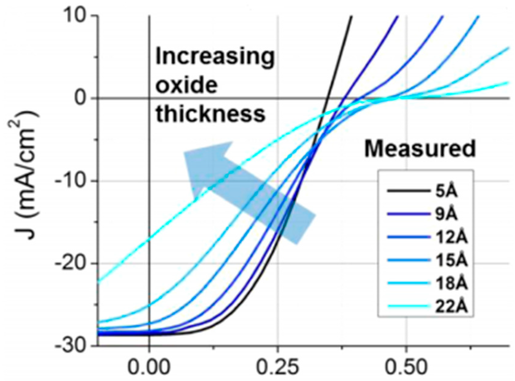
1. Introduction
2. Materials and Methods
3. Results and Discussion
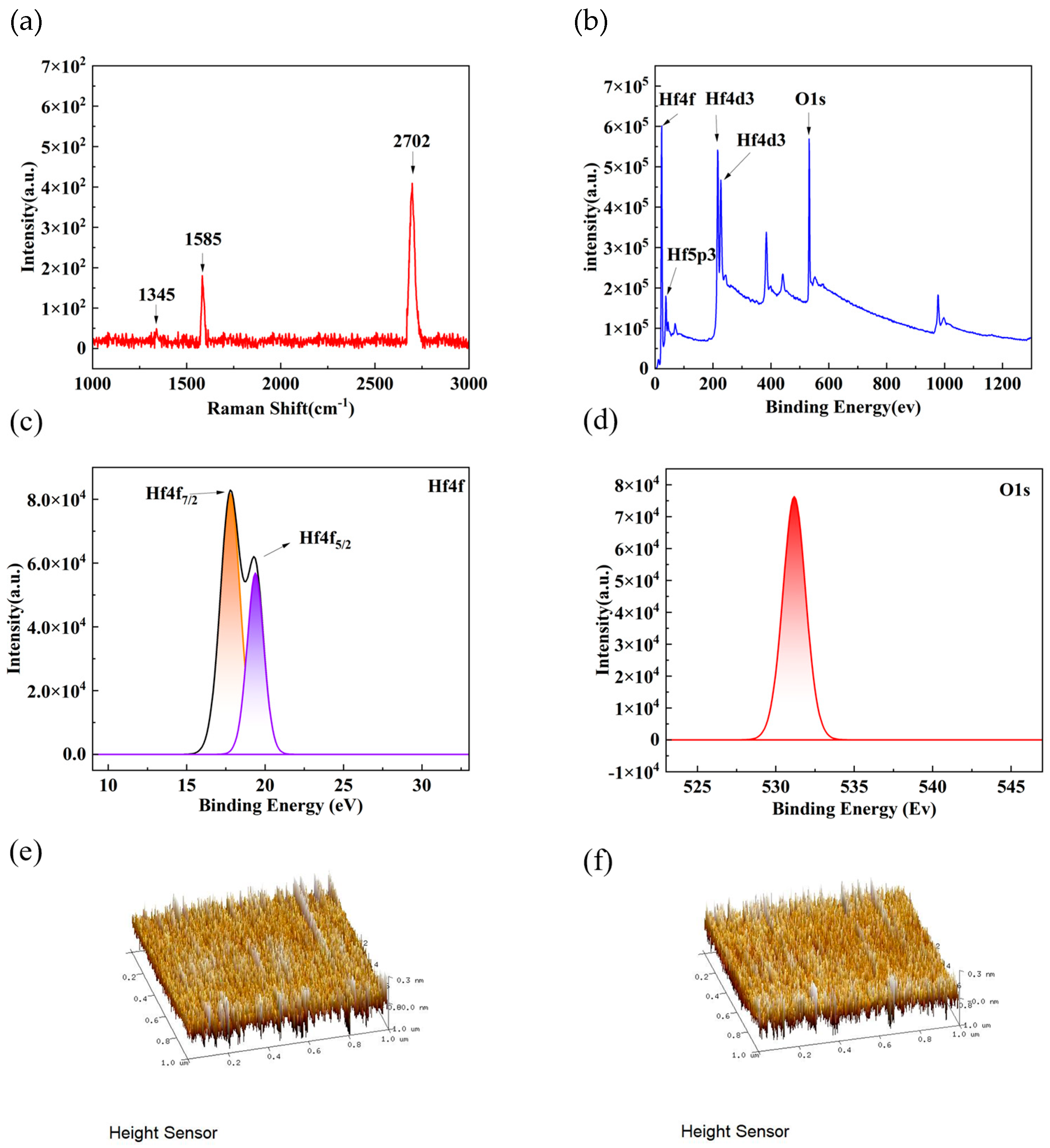
3.1. Characterization of Materials and Devices
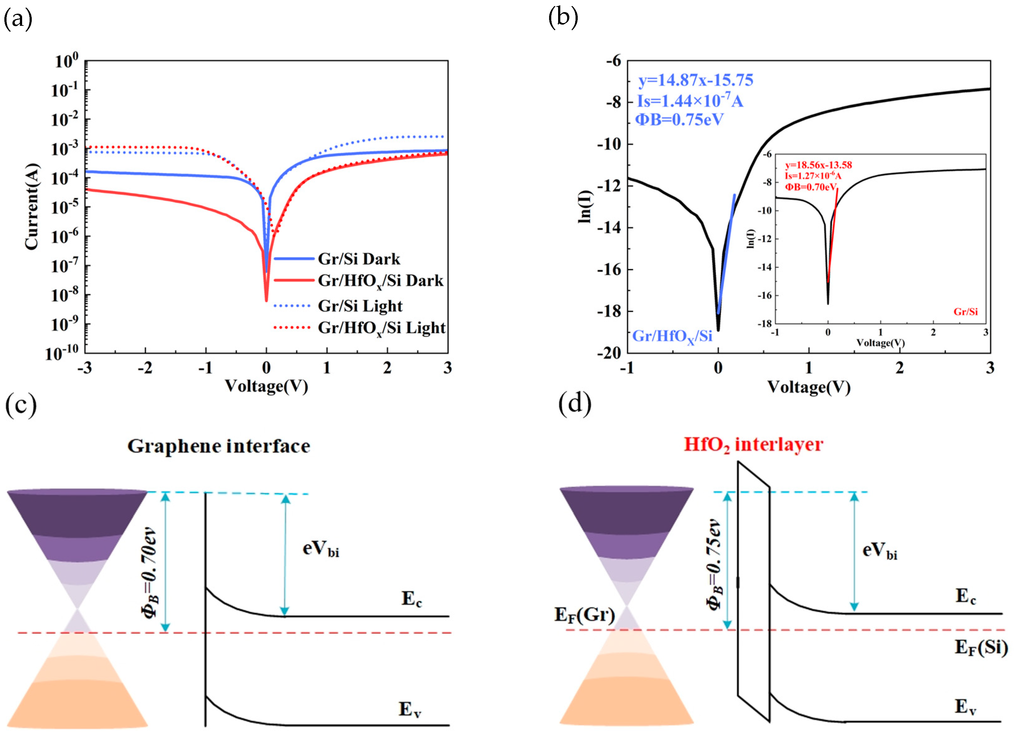
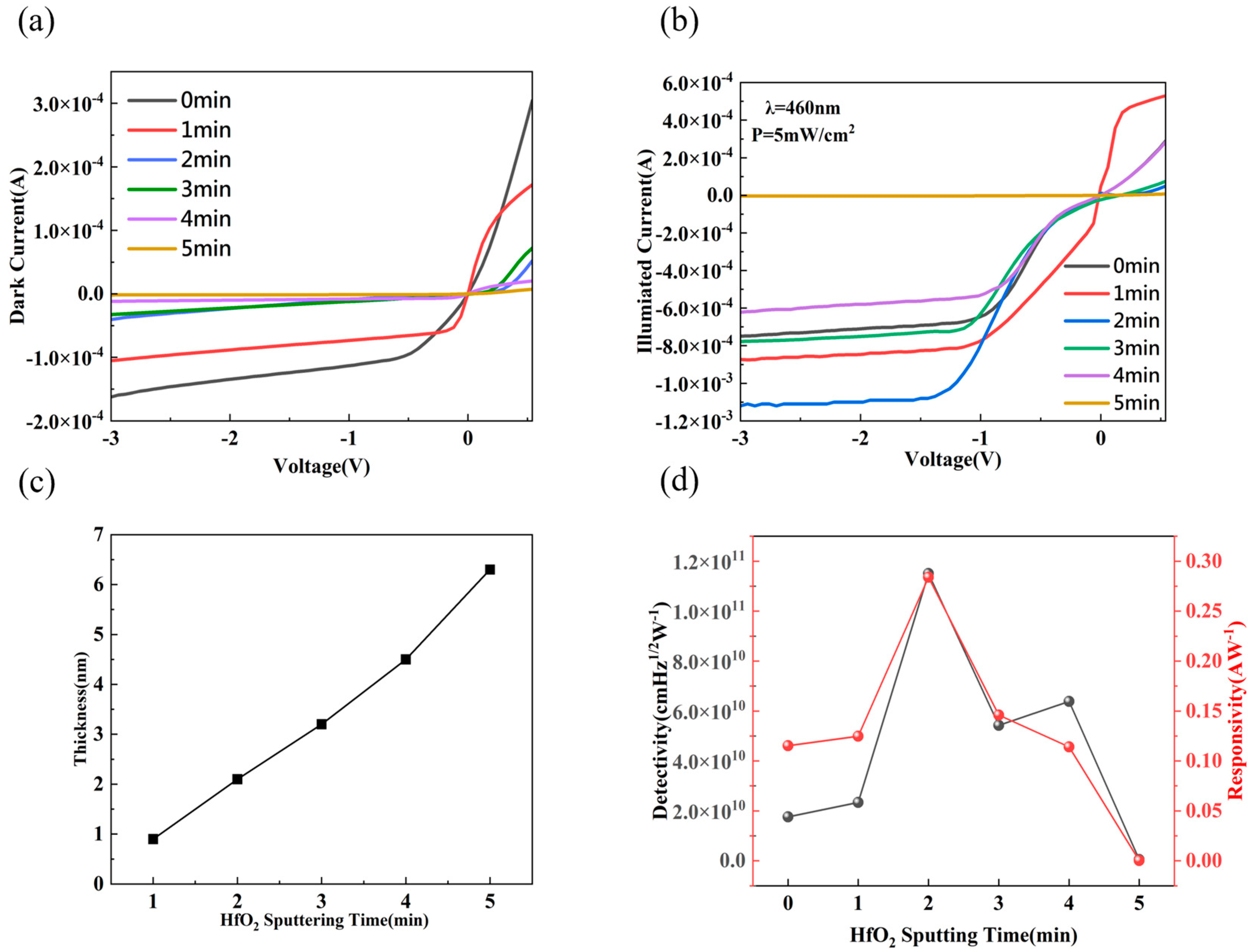
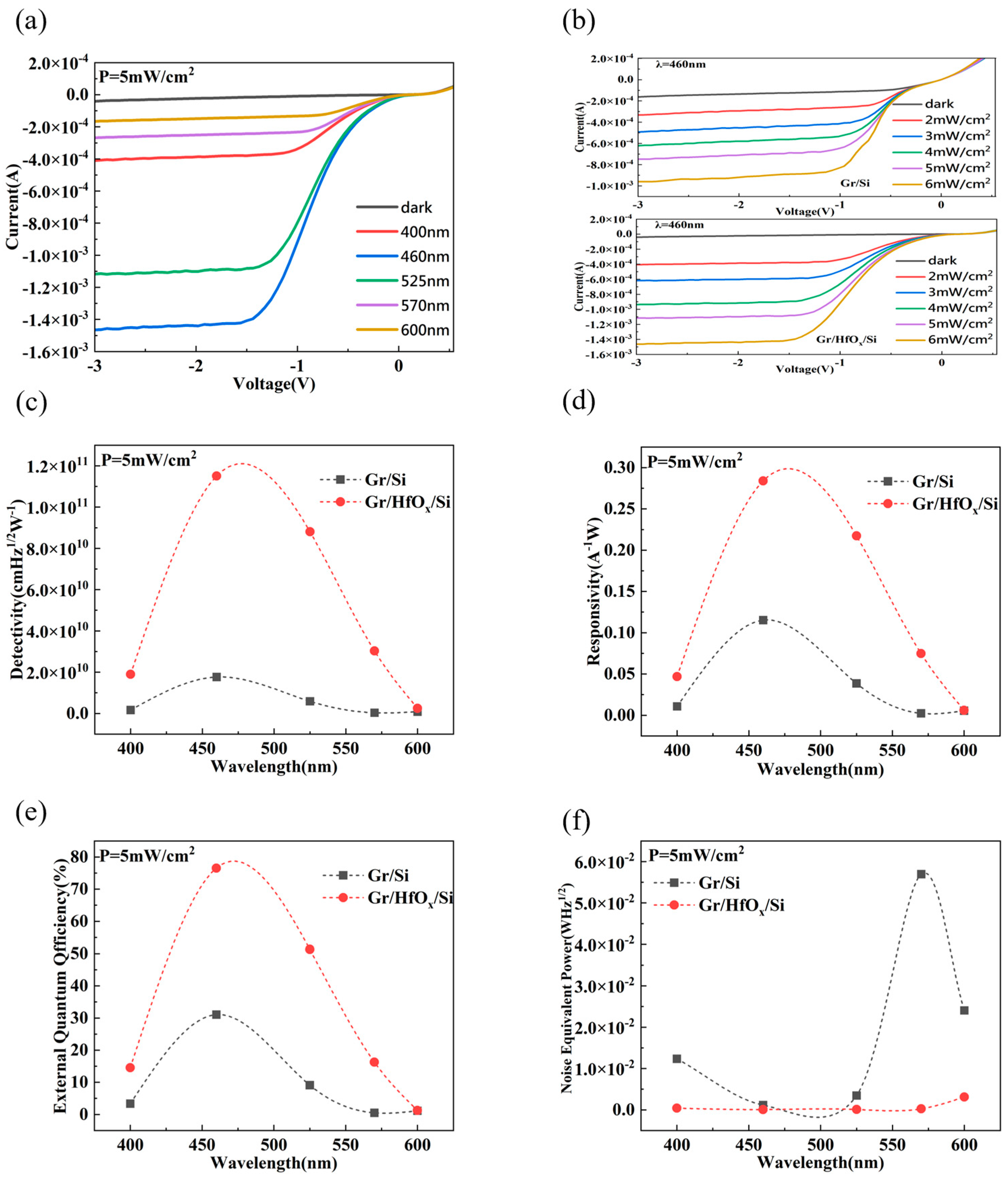
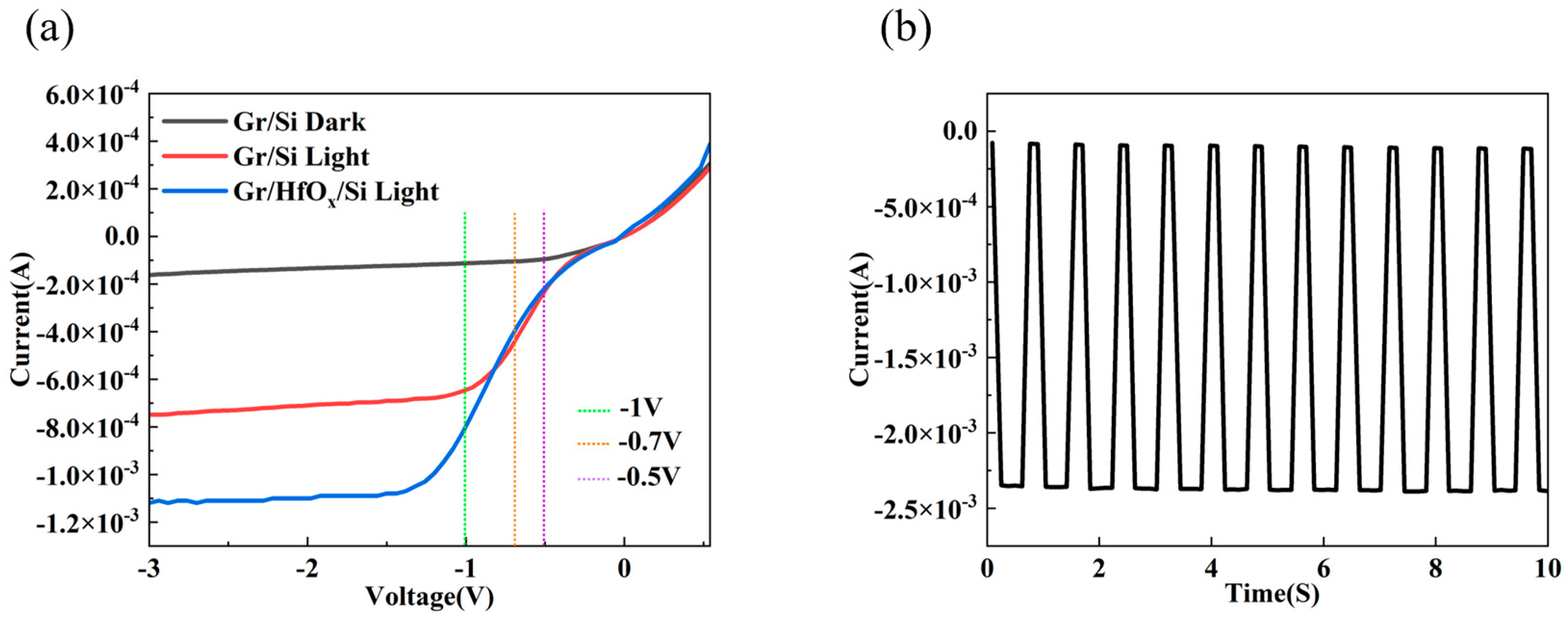
3.2. Performance of Gr/HfOx/Si Schottky Photodetector
4. Conclusions
Author Contributions
Funding
Data Availability Statement
Conflicts of Interest
References
- Li, J.F.; Zhao, C.; Liu, B.Y.; You, C.Y.; Chu, F.H.; Tian, N.; Chen, Y.F.; Li, S.Y.; An, B.X.; Cui, A.J.; et al. Metamaterial grating-integrated graphene photodetector with broadband high responsivity. Appl. Surf. Sci. 2019, 473, 633–640. [Google Scholar] [CrossRef]
- Qian, Z.Y.; Hui, Y.; Liu, F.Z.; Kang, S.H.; Kar, S.; Rinaldi, M. Graphene-aluminum nitride NEMS resonant infrared detector. Microsyst. Nanoeng. 2016, 2, 16026. [Google Scholar] [CrossRef] [PubMed]
- Wang, R.X.; Yang, L.C.; Zhang, Y.M.; Xu, S.J.; Fu, K.; Zhang, B.S.; Wang, J.F.; Xu, K.; Yang, H. The effect of Ga-doped nanocrystalline ZnO electrode on deep-ultraviolet enhanced GaN photodetector. Appl. Phys. Lett. 2013, 102, 212104. [Google Scholar] [CrossRef]
- Huang, Z.; Carey, J.E.; Liu, M.; Guo, X.; Mazur, E.; Campbell, J.C. Microstructured silicon photodetector. Appl. Phys. Lett. 2006, 89, 033506. [Google Scholar] [CrossRef]
- Zang, K.; Zhang, D.K.; Huo, Y.J.; Chen, X.C.; Lu, C.Y.; Fei, E.T.; Kamins, T.I.; Feng, X.; Huang, Y.D.; Harris, J.S. Microring bio-chemical sensor with integrated low dark current Ge photodetector. Appl. Phys. Lett. 2015, 106, 101111. [Google Scholar] [CrossRef]
- Kopytko, M.; Keblowski, A.; Gawron, W.; Madejczyk, P.; Kowalewski, A.; Jozwikowski, K. High-operating temperature MWIR nBn HgCdTe detector grown by MOCVD. Opto-Electron. Rev. 2013, 21, 402–405. [Google Scholar] [CrossRef]
- Yang, Q.; Wu, Q.M.; Luo, W.; Yao, W.; Yan, S.Y.; Shen, J. InGaAs/graphene infrared photodetectors with enhanced responsivity. Mater. Res. Express 2019, 6, 116208. [Google Scholar] [CrossRef]
- Shao, Q.G.; Qi, H.; Li, C.; Cai, K.P.; Dong, J.X.; Liu, X.H.; Cao, N.; Zang, X.B. Recent Progress of Gr/Si Schottky Photodetectors. Electron. Mater. Lett. 2023, 19, 121–137. [Google Scholar] [CrossRef]
- Gnisci, A.; Faggio, G.; Lancellotti, L.; Messina, G.; Carotenuto, R.; Bobeico, E.; Veneri, P.D.; Capasso, A.; Dikonimos, T.; Lisi, N.J.J.W.; et al. The Role of Graphene-Based Derivative as Interfacial Layer in Graphene/n-Si Schottky Barrier Solar Cells. Appl. Mater. Sci. 2019, 216, 1800555. [Google Scholar] [CrossRef]
- Xu, J.; Liu, T.; Hu, H.; Zhai, Y.S.; Chen, K.; Chen, N.; Li, C.; Zhang, X.B. Design and optimization of tunneling photodetectors based on graphene/Al2O3/silicon heterostructures. Nanophotonics 2020, 9, 3841–3848. [Google Scholar] [CrossRef]
- Song, Y.; Li, X.M.; Mackin, C.; Zhang, X.; Fang, W.J.; Palacios, T.; Zhu, H.W.; Kong, J. Role of Interfacial Oxide in High-Efficiency Graphene-Silicon Schottky Barrier Solar Cells. Nano Lett. 2015, 15, 2104–2110. [Google Scholar] [CrossRef] [PubMed]
- Kavrik, M.S.; Ercius, P.; Cheung, J.; Tang, K.; Wang, Q.; Fruhberger, B.; Kim, M.; Taur, Y.; McIntyre, P.C.; Kummel, A.C. Engineering High-k/SiGe Interface with ALD Oxide for Selective GeOx Reduction. ACS Appl. Mater. Interfaces 2019, 11, 15111–15121. [Google Scholar] [CrossRef] [PubMed]
- Qi, M.; Fu, T.; Yang, H.; Tao, Y.; Li, C.; Xiu, X. Reliable analog resistive switching behaviors achieved using memristive devices in AlOx/HfOx bilayer structure for neuromorphic systems. Semicond. Sci. Technol. 2022, 37, 035018. [Google Scholar] [CrossRef]
- Tan, R.Q.; Azuma, Y.; Kojima, I. Comparative study of the interfacial characteristics of sputter-deposited HfO2 on native SiO2/Si (100) using XPS, AES and GIXR. Surf. Interface Anal. 2006, 38, 784–788. [Google Scholar] [CrossRef]
- Nath, M.; Roy, A. Interface and electrical properties of ultra-thin HfO2 film grown by radio frequency sputtering. Physica B 2016, 482, 43–50. [Google Scholar] [CrossRef]
- Szymanska, M.; Gieraltowska, S.; Wachnicki, L.; Grobelny, M.; Makowska, K.; Mroczynski, R. Effect of reactive magnetron sputtering parameters on structural and electrical properties of hafnium oxide thin films. Appl. Surf. Sci. 2014, 301, 28–33. [Google Scholar] [CrossRef]
- Tan, T.T.; Chen, X.; Guo, T.T.; Liu, Z.T. Bipolar Resistive Switching Characteristics of TiN/HfOx/ITO Devices for Resistive Random Access Memory Applications. Chin. Phys. Lett. 2013, 30, 107302. [Google Scholar] [CrossRef]
- Li, F.M.; Bayer, B.C.; Hofmann, S.; Speakman, S.P.; Ducati, C.; Milne, W.I.; Flewitt, A.J. High-density remote plasma sputtering of high-dielectric-constant amorphous hafnium oxide films. Phys. Status Solidi B-Basic Solid State Phys. 2013, 250, 957–967. [Google Scholar] [CrossRef]
- Card, H.C.; Rhoderick, E.H. Studies of tunnel MOS diodes I. Interface effects in silicon Schottky diodes. J. Phys. D Appl. Phys. 1971, 4, 1589. [Google Scholar] [CrossRef]
- Cheung, S.K.; Cheung, N.W. Extraction of Schottky diode parameters from forward current-voltage characteristics. Appl. Phys. Lett. 1986, 49, 85–87. [Google Scholar] [CrossRef]
- Rehman, M.A.; Akhtar, I.; Choi, W.; Akbar, K.; Farooq, A.; Hussain, S.; Shehzad, M.A.; Chun, S.H.; Jung, J.; Seo, Y. Influence of an Al2O3 interlayer in a directly grown graphene-silicon Schottky junction solar cell. Carbon 2018, 132, 157–164. [Google Scholar] [CrossRef]
- Tao, L.; Chen, Z.F.; Li, X.M.; Yan, K.Y.; Xu, J.B. Hybrid graphene tunneling photoconductor with interface engineering towards fast photoresponse and high responsivity. npj 2d Mater. Appl. 2017, 1, 19. [Google Scholar] [CrossRef]
- Ji, P.R.; Yang, S.M.; Wang, Y.; Li, K.L.; Wang, Y.M.; Suo, H.; Woldu, Y.T.; Wang, X.M.; Wang, F.; Zhang, L.L.; et al. High-performance photodetector based on an interface engineering-assisted graphene/silicon Schottky junction. Microsyst. Nanoeng. 2022, 8, 9. [Google Scholar] [CrossRef] [PubMed]
- Xu, D.K.; Yu, X.G.; Yang, L.F.; Yang, D.R. Design and Photovoltaic Properties of Graphene/Silicon Solar Cell. J. Electron. Mater. 2018, 47, 5025–5032. [Google Scholar] [CrossRef]
- Jiao, T.P.; Wei, D.P.; Song, X.F.; Sun, T.; Yang, J.; Yu, L.Y.; Feng, Y.H.; Sun, W.T.; Wei, W.; Shi, H.F.; et al. High-efficiency, stable and non-chemically doped graphene-Si solar cells through interface engineering and PMMA antireflection. RSC Adv. 2016, 6, 10175–10179. [Google Scholar] [CrossRef]
- Wang, Y.M.; Yang, S.M.; Lambada, D.R.; Shafique, S. A graphene-silicon Schottky photodetector with graphene oxide interlayer. Sens. Actuator A-Phys. 2020, 314, 112232. [Google Scholar] [CrossRef]
- Yang, L.F.; Yu, X.G.; Xu, M.S.; Chen, H.Z.; Yang, D.R. Interface engineering for efficient and stable chemical-doping-free graphene-on-silicon solar cells by introducing a graphene oxide interlayer. J. Mater. Chem. A 2014, 2, 16877–16883. [Google Scholar] [CrossRef]
- Aydin, H.; Kalkan, S.B.; Varlikli, C.; Çelebi, C. P3HT-graphene bilayer electrode for Schottky junction photodetectors. Nanotechnology 2018, 29, 145502. [Google Scholar] [CrossRef]
- Li, X.M.; Zhu, M.; Du, M.D.; Lv, Z.; Zhang, L.; Li, Y.C.; Yang, Y.; Yang, T.T.; Li, X.; Wang, K.L.; et al. High Detectivity Graphene-Silicon Heterojunction Photodetector. Small 2016, 12, 595–601. [Google Scholar] [CrossRef]
- An, X.H.; Liu, F.Z.; Jung, Y.J.; Kar, S. Tunable Graphene-Silicon Heterojunctions for Ultrasensitive Photodetection. Nano Lett. 2013, 13, 909–916. [Google Scholar] [CrossRef]
- Cong, J.K.; Khan, A.; Hang, P.J.; Cheng, L.; Yang, D.R.; Yu, X.G. High detectivity graphene/si heterostructure photodetector with a single hydrogenated graphene atomic interlayer for passivation and carrier tunneling. Nanotechnology 2022, 33, 505201. [Google Scholar] [CrossRef]
- Won, U.Y.; Lee, B.H.; Kim, Y.R.; Kang, W.T.; Lee, I.; Kim, J.E.; Lee, Y.H.; Yu, W.J. Efficient photovoltaic effect in graphene/h-BN/silicon heterostructure self-powered photodetector. Nano Res. 2021, 14, 1967–1972. [Google Scholar] [CrossRef]


| Device Structure | λ nm | Responsivity A/W | D* Jones | NEP pW/Hz1/2 | Idark nA | EQE(%) | Ref. |
|---|---|---|---|---|---|---|---|
| Gr/HfOx/Si | 460 | 0.284 | 1.15 × 10¹¹ | 8.75 × 10⁻⁵ | 6.15 | 76.5 | this work |
| Gr/Si | 890 | 0.73 | 4.2 × 10¹² | 0.075 | 9.3 | 65.0 | [29] |
| Gr/Si | 730 | 0.435 | 2.1 × 10⁸ | 33 | [30] | ||
| Gr/Al2O3/Si | 658 | 0.75 | 3.1 × 10¹² | [10] | |||
| Gr/H-Gr/Si | 532 | 0.245 | 2.3 × 10¹¹ | 100 | [31] | ||
| Gr/h-BN/Si | 725 | 2.83 × 10¹⁰ | [32] | ||||
| P3HT–Gr/Si | 540 | 0.78 | 2.6 × 10¹⁰ | 0.14 | 40 | [28] |
Disclaimer/Publisher’s Note: The statements, opinions and data contained in all publications are solely those of the individual author(s) and contributor(s) and not of MDPI and/or the editor(s). MDPI and/or the editor(s) disclaim responsibility for any injury to people or property resulting from any ideas, methods, instructions or products referred to in the content. |
© 2024 by the authors. Licensee MDPI, Basel, Switzerland. This article is an open access article distributed under the terms and conditions of the Creative Commons Attribution (CC BY) license (https://creativecommons.org/licenses/by/4.0/).
Share and Cite
Qu, T.; Fan, J.; Wei, X. Dark Current Reduction and Performance Improvements in Graphene/Silicon Heterojunction Photodetectors Obtained Using a Non-Stoichiometric HfOx Thin Oxide Layer. Nanomaterials 2024, 14, 419. https://doi.org/10.3390/nano14050419
Qu T, Fan J, Wei X. Dark Current Reduction and Performance Improvements in Graphene/Silicon Heterojunction Photodetectors Obtained Using a Non-Stoichiometric HfOx Thin Oxide Layer. Nanomaterials. 2024; 14(5):419. https://doi.org/10.3390/nano14050419
Chicago/Turabian StyleQu, Tao, Jibin Fan, and Xing Wei. 2024. "Dark Current Reduction and Performance Improvements in Graphene/Silicon Heterojunction Photodetectors Obtained Using a Non-Stoichiometric HfOx Thin Oxide Layer" Nanomaterials 14, no. 5: 419. https://doi.org/10.3390/nano14050419
APA StyleQu, T., Fan, J., & Wei, X. (2024). Dark Current Reduction and Performance Improvements in Graphene/Silicon Heterojunction Photodetectors Obtained Using a Non-Stoichiometric HfOx Thin Oxide Layer. Nanomaterials, 14(5), 419. https://doi.org/10.3390/nano14050419