
Diamond for High-Power, High-Frequency, and Terahertz Plasma Wave Electronics


Abstract
:1. Introduction
2. Electronic Material Properties of Diamond
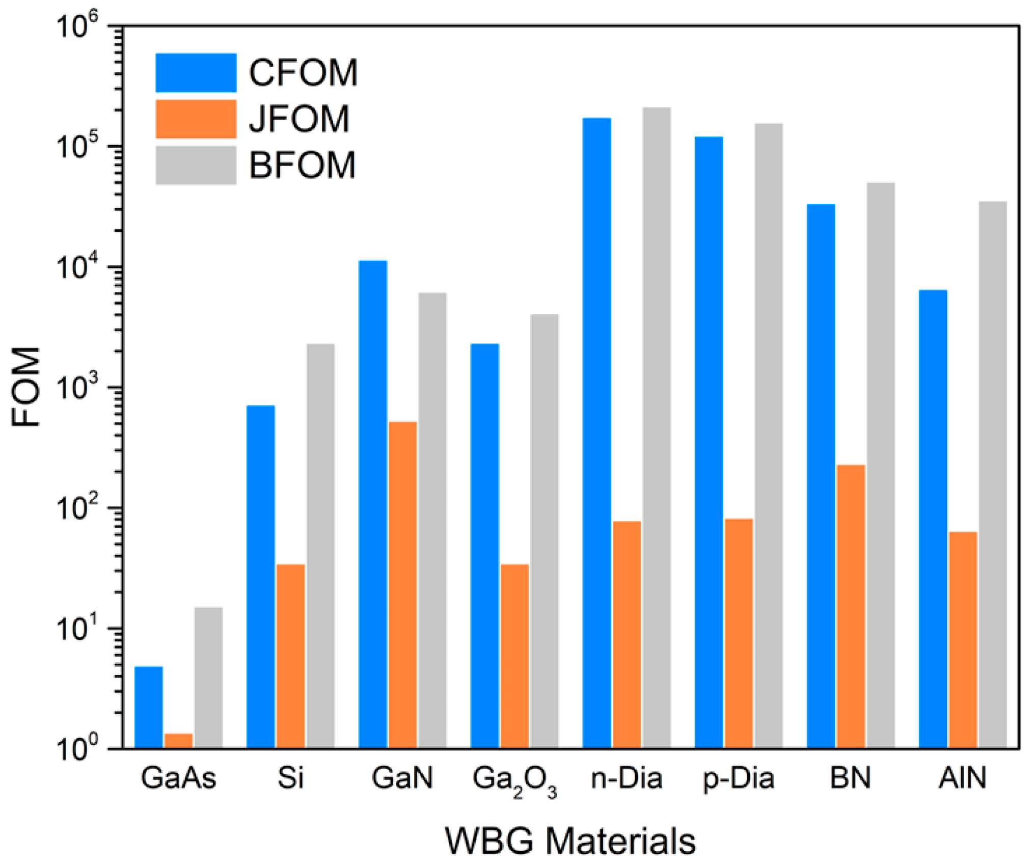
2.1. Comparison Figures of Merit

| Material Properties | GaAs | Si | 4H-SiC | GaN | BN | AlN | Ga2O3 | Diamond | Comment |
|---|---|---|---|---|---|---|---|---|---|
| Energy bandgap (eV) | 1.42 | 1.1 | 3.2 | 3.44 | 6.4 | 6.2 | 4.8 | 5.47 | High-temperature operation |
| Dielectric constant | 12.9 | 11.8 | 9.7 | 9 | 7.1 | 9.76 | 10 | 5.7 | - |
| Breakdown field (MV cm−1) | 0.4 | 0.3 | 3 | 5 | 17.5 | 15.4 | 8 | 10 | High voltage applications |
| Effective mass | 0.067 | 0.19 | 0.24 | 0.43 | 0.4 | 0.297 | 0.74 (hole) 0.36 (electron) | Long momentum relaxation time | |
| Thermal conductivity (Wm−1 K−1) | 55 | 150 | 500 | 130 | 2145 | 1000 | 27 | 2200 | High-power applications |
| Electron saturation velocity (cm s−1) | 1.1 × 10⁷ | 0.86 × 10⁷ | 3 × 10⁷ | 2.5 × 10⁷ | 4.3 × 10⁷ | 1.3 × 10⁷ | 2 × 10⁷ | 2.7 × 10⁷ | |
| Hole saturation velocity (cm s−1) | - | 0.8 × 10⁷ | 1.2 × 10⁷ | - | - | - | - | 1.2 × 10⁷ | High-frequency operation |
| Electron mobility (cm2 V−1 s−1) | 8500 | 1450 | 900 | 440 | 825 | 426 | 300 | 7300 | |
| Hole mobility (cm2 V−1 s−1) | - | 480 | 120 | 200 | 500 | - | - | 5300 | |
| BFOM | 15 | 1 | 554 | 188 | - | 35,497 | 3214 | 23,068 | Power handling capability |
| CFOM | 5 | 1 | 594 | 162 | - | 6518 | 53 | 124,424 | |
| BHFOM | - | 1 | 58 | 237 | - | - | 158 | 12,510 | Takes switching losses into account |
| JFOM (1023 ΩW s−2) | 1.36 | 2.3 | 900 | 490 | - | 64 | 1236 | 2530 | RF power capacity |
| KFOM (107 WK−1 s−1) | - | 10 | 53 | 17 | - | - | 2 | 218 | Thermal limit of transistor characteristics |
| HMFOM | - | 2 | - | 18 | - | - | 22 | 72 | |
| HCAFOM | - | 1 | 58 | 192 | - | - | 280 | 3887 | Reduction of chip area |
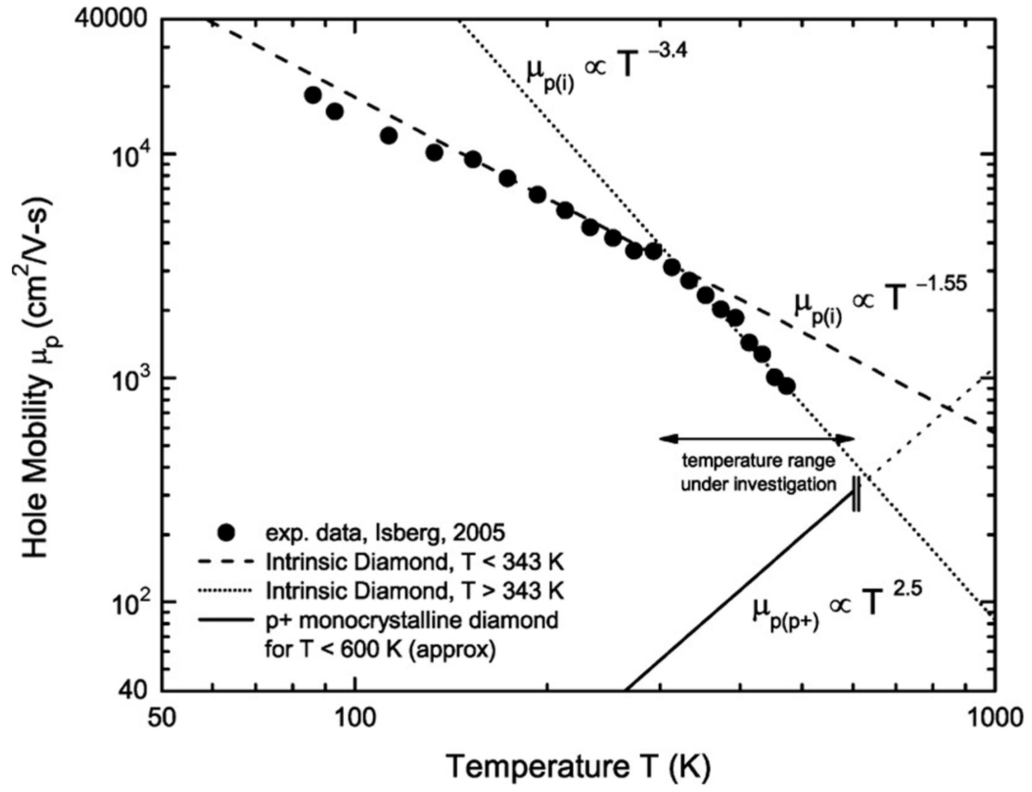
2.2. Carrier Mobility
2.3. Thermal Properties
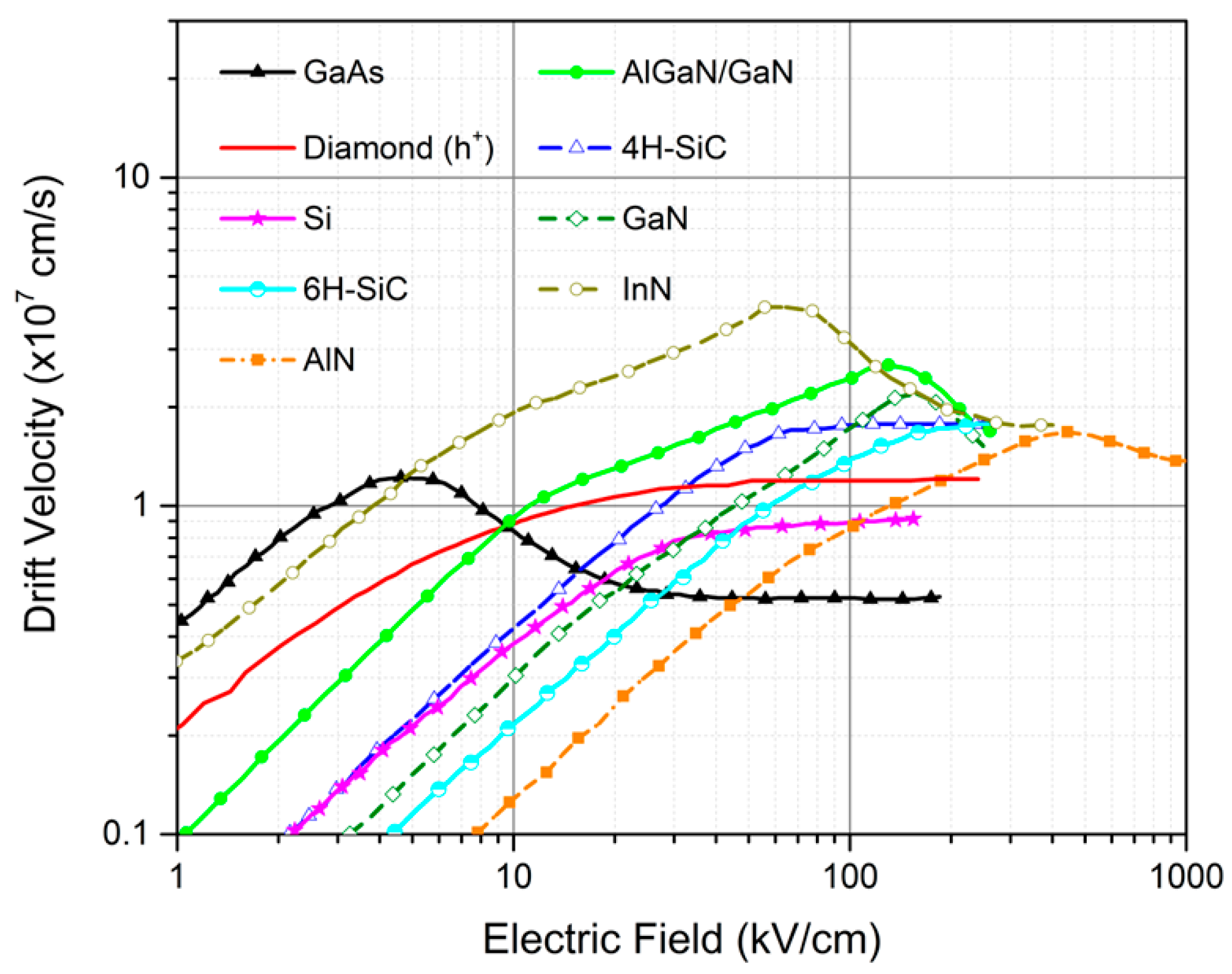
2.4. Saturation Velocity of Carriers
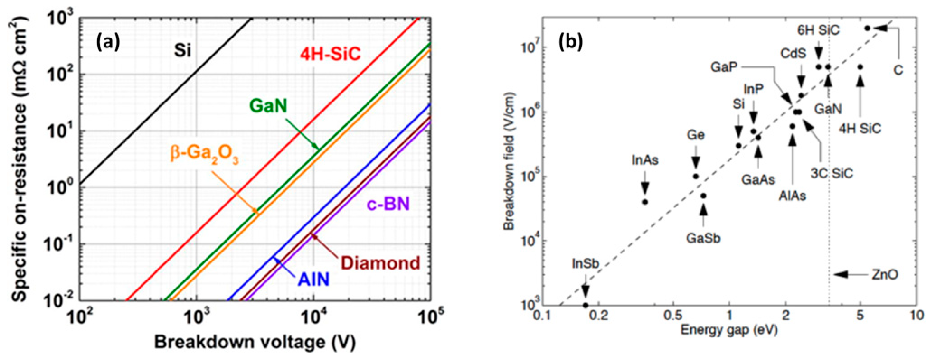
2.5. Breakdown Field
2.6. Carrier Lifetime
3. Material Quality and Growth Techniques
3.1. Substrate Quality
3.2. Diamond Growth Technologies
3.2.1. Diamond Growth by HPHT
3.2.2. Diamond Growth by CVD
3.3. Doping
3.3.1. P-Type Doping
3.3.2. N-Type Doping
3.3.3. Surface Transfer Doping
4. Diamond-Based High-Power Electronic Devices
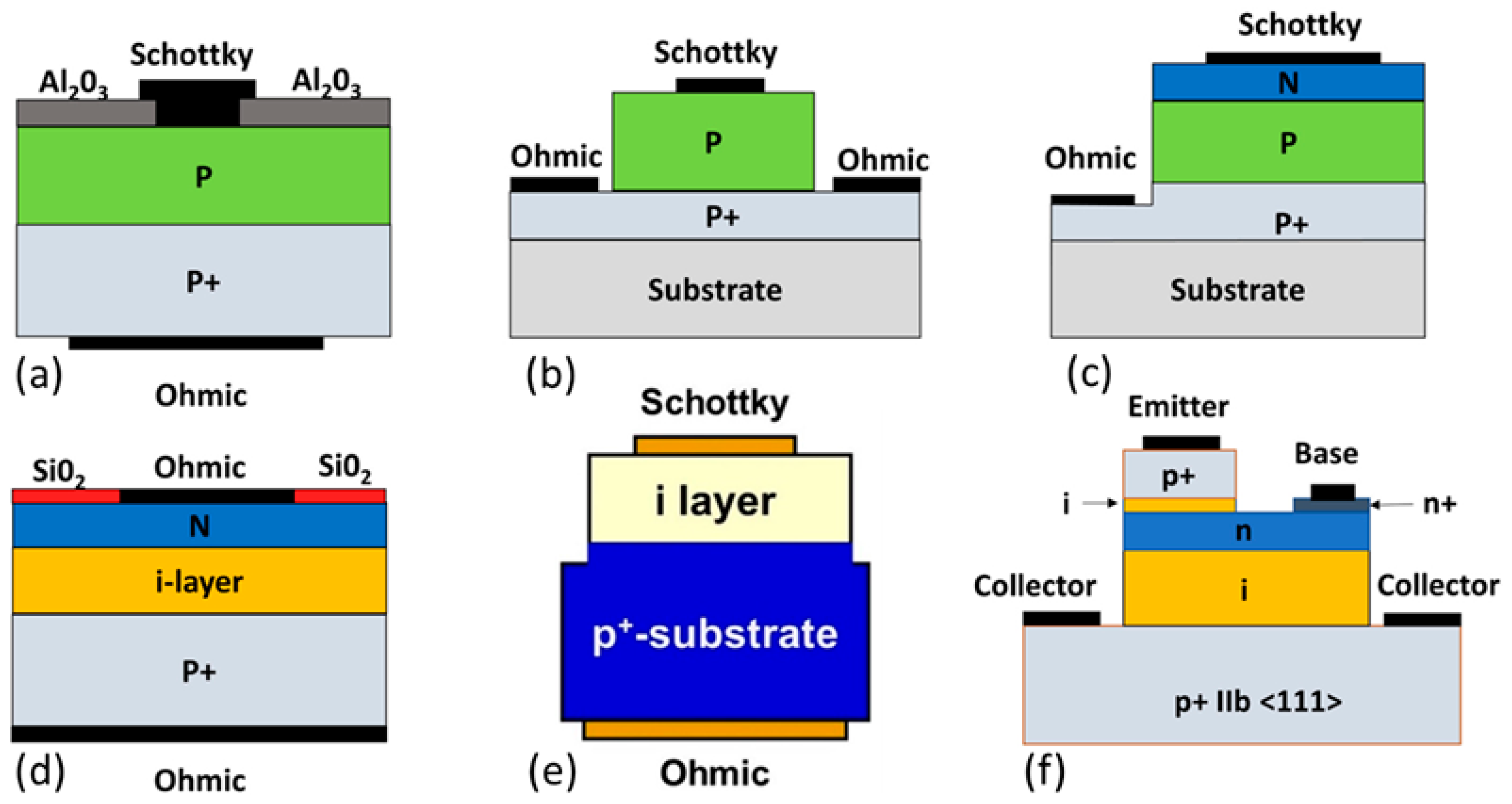
4.1. Schottky, Diodes, and Bipolar Junction Transistors (BJTs)
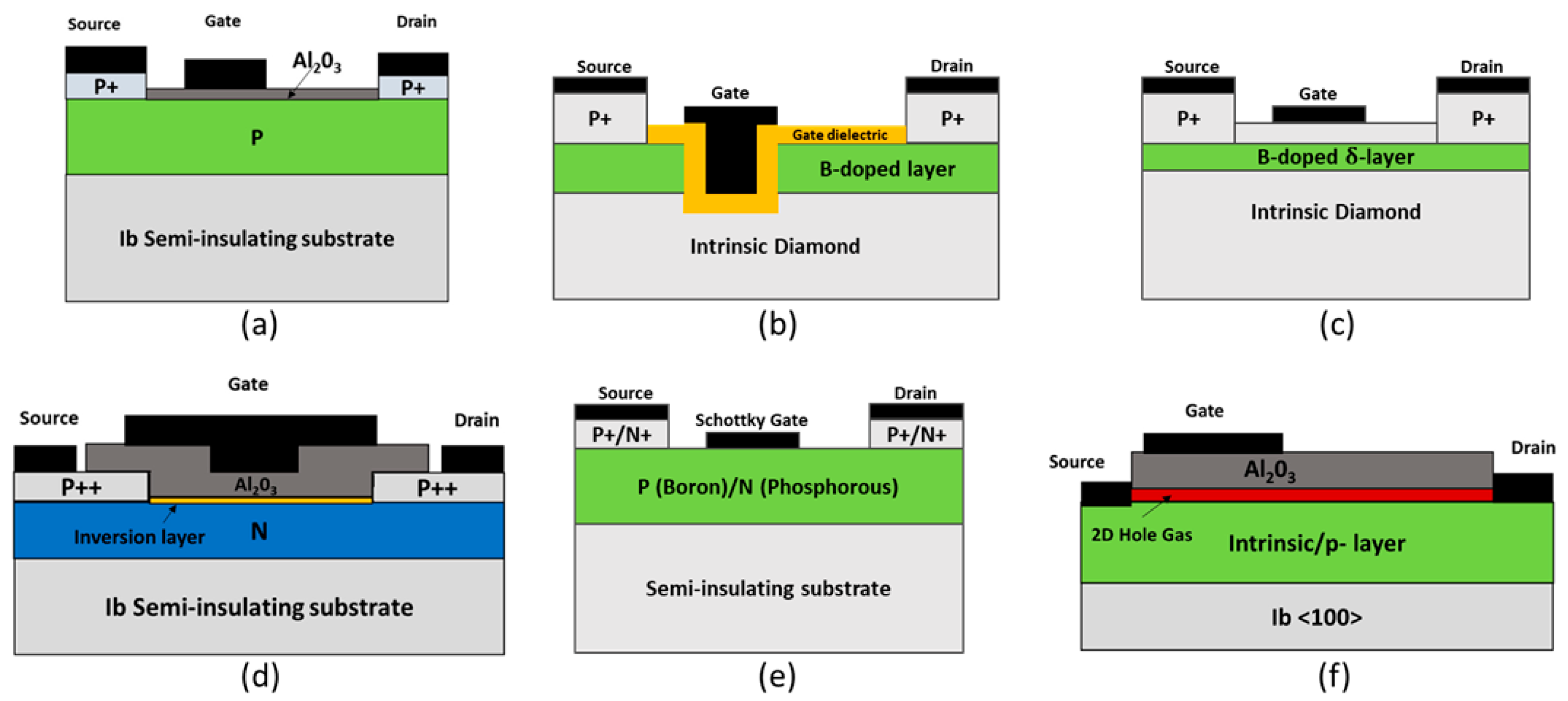
4.2. Diamond Field Effect Transistors
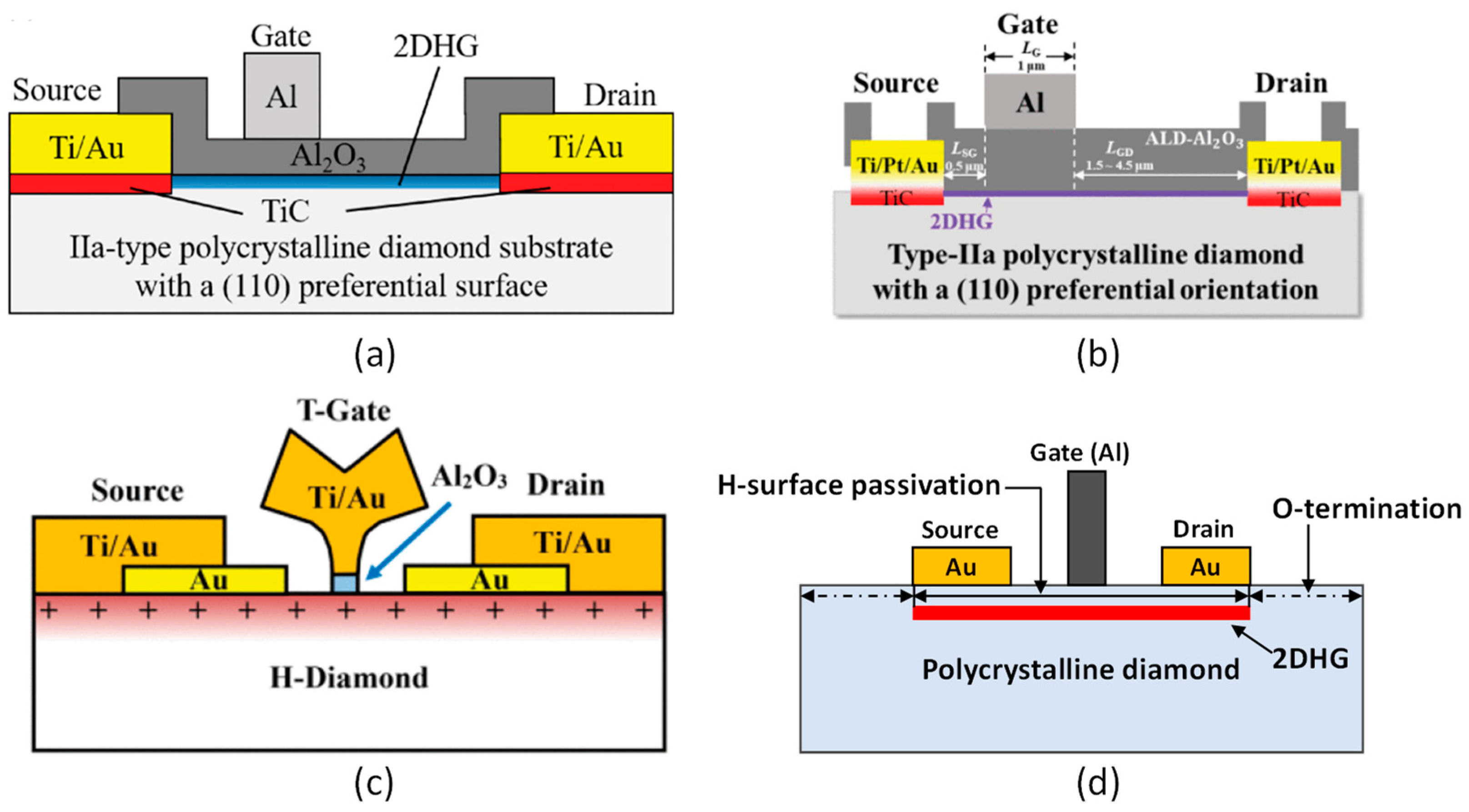
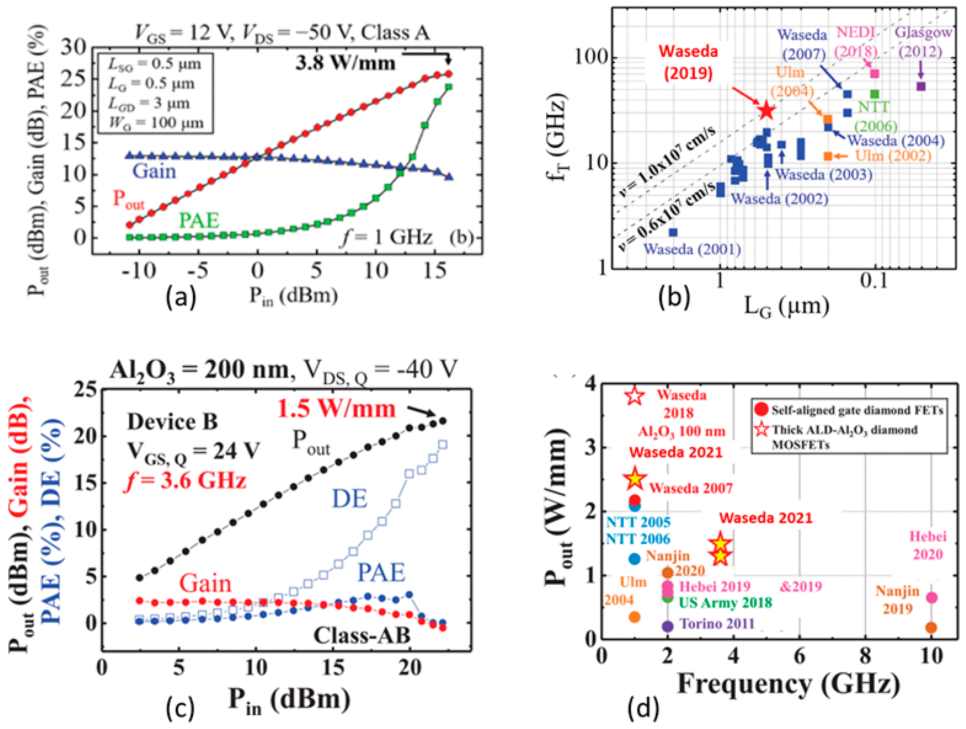
5. Diamond-Based High-Frequency Devices
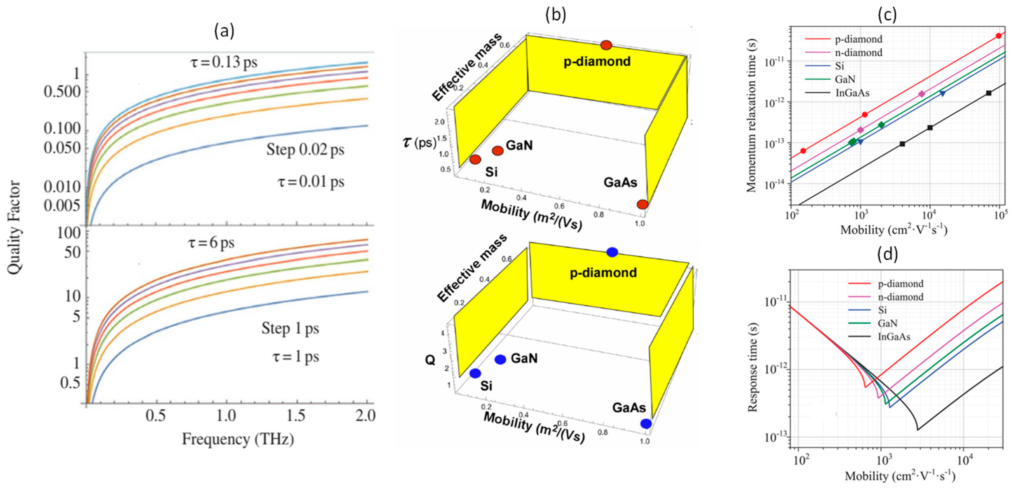
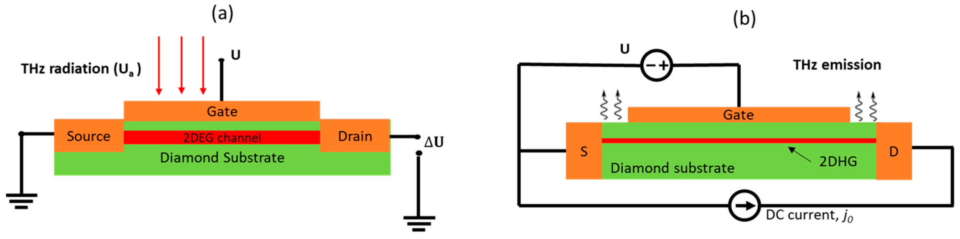
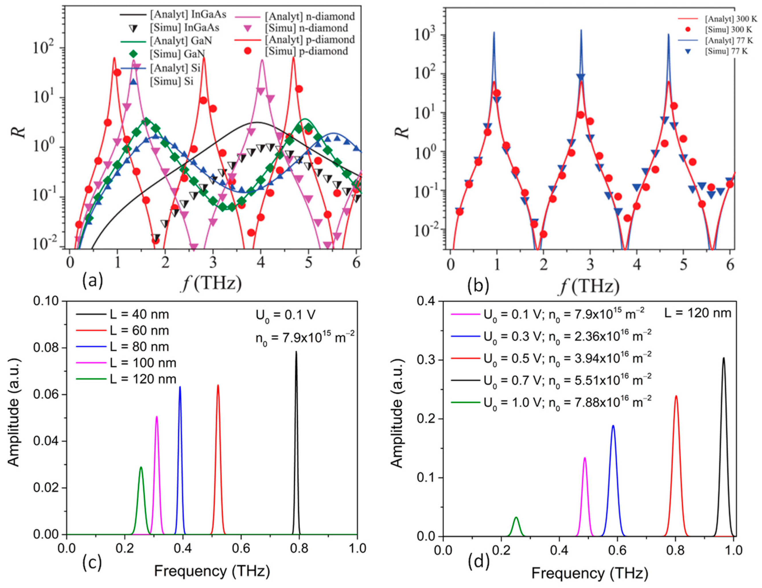
6. Plasma Wave in Diamond Terahertz Field Effect Transistors (Diamond TeraFETs)
6.1. Hydrodynamic Model
6.2. Diamond Properties for THz Detection and Emission
6.3. Terahertz Detection and Emission by Diamond TeraFET
7. Conclusions
Author Contributions
Funding
Conflicts of Interest
References
- Shur, M.; Aizin, G.; Otsuji, T.; Ryzhii, V. Plasmonic field-effect transistors (TeraFETs) for 6G communications. Sensors 2021, 21, 7907. [Google Scholar] [CrossRef] [PubMed]
- Veksler, D.; Muraviev, A.; Elkhatib, T.; Salama, K.; Shur, M. Plasma wave FET for sub-wavelength THz imaging. In Proceedings of the 2007 International Semiconductor Device Research Symposium, College Park, MD, USA, 12–14 December 2007; pp. 1–2. [Google Scholar]
- Federici, J.F.; Schulkin, B.; Huang, F.; Gary, D.; Barat, R.; Oliveira, F.; Zimdars, D. THz imaging and sensing for security applications—Explosives, weapons and drugs. Semicond. Sci. Technol. 2005, 20, S266. [Google Scholar] [CrossRef]
- Shur, M.; Rudin, S.; Rupper, G.; Reed, M.; Suarez, J. Sub-terahertz testing of millimeter wave monolithic and very large scale integrated circuits. Solid-State Electron. 2019, 155, 44–48. [Google Scholar] [CrossRef]
- Rumyantsev, S.L.; Muraviev, A.; Rudin, S.; Rupper, G.; Reed, M.; Suarez, J.; Shur, M. Terahertz beam testing of millimeter wave monolithic integrated circuits. IEEE Sens. J. 2017, 17, 5487–5491. [Google Scholar] [CrossRef]
- O’Hara, J.F.; Ekin, S.; Choi, W.; Song, I. A perspective on terahertz next-generation wireless communications. Technologies 2019, 7, 43. [Google Scholar] [CrossRef]
- Shur, M. Plasmonic detectors and sources for THz communication and sensing. In Proceedings of the Micro-and Nanotechnology Sensors, Systems, and Applications X, Orlando, FL, USA, 15–19 April 2018; International Society for Optics and Photonics: Bellingham, WA, USA, 2018; p. 1063929. [Google Scholar]
- Akter, N.; Hasan, M.M.; Pala, N. A review of THz technologies for rapid sensing and detection of viruses including SARS-CoV-2. Biosensors 2021, 11, 349. [Google Scholar] [CrossRef]
- Olatinwo, D.D.; Abu-Mahfouz, A.; Hancke, G. A survey on LPWAN technologies in WBAN for remote health-care monitoring. Sensors 2019, 19, 5268. [Google Scholar] [CrossRef] [PubMed]
- Levinshteĭn, M.E.; Rumyantsev, S.; Shur, M. Si, Ge, C (Diamond), GaAs, GaP, GaSb, InAs, InP, InSb. In Handbook Series on Semiconductor Parameters; World Scientific Publishing: Singapore, 1996. [Google Scholar]
- Arnault, J.-C.; Saada, S.; Ralchenko, V. Chemical vapor deposition single-crystal diamond: A review. Phys. Status Solidi (RRL)–Rapid Res. Lett. 2022, 16, 2100354. [Google Scholar] [CrossRef]
- Makino, T.; Oyama, K.; Kato, H.; Takeuchi, D.; Ogura, M.; Okushi, H.; Yamasaki, S. Diamond electronic devices fabricated using heavily doped hopping p+ and n+ layers. Jpn. J. Appl. Phys. 2014, 53, 05FA12. [Google Scholar] [CrossRef]
- Kato, H.; Makino, T.; Ogura, M.; Tokuda, N.; Okushi, H.; Yamasaki, S. Selective growth of buried n+ diamond on (001) phosphorus-doped n-type diamond film. Appl. Phys. Express 2009, 2, 055502. [Google Scholar] [CrossRef]
- Ueda, K.; Kasu, M.; Yamauchi, Y.; Makimoto, T.; Schwitters, M.; Twitchen, D.; Scarsbrook, G.; Coe, S. Diamond FET using high-quality polycrystalline diamond with f T of 45 GHz and f max of 120 GHz. IEEE Electron Device Lett. 2006, 27, 570–572. [Google Scholar] [CrossRef]
- Yu, X.; Zhou, J.; Qi, C.; Cao, Z.; Kong, Y.; Chen, T. A High Frequency Hydrogen-Terminated Diamond MISFET with Al2O3 of 70/80 GHz. IEEE Electron Device Lett. 2018, 39, 1373–1376. [Google Scholar] [CrossRef]
- Imanishi, S.; Horikawa, K.; Oi, N.; Okubo, S.; Kageura, T.; Hiraiwa, A.; Kawarada, H. 3.8 W/mm RF power density for ALD Al 2 O 3-based two-dimensional hole gas diamond MOSFET operating at saturation velocity. IEEE Electron Device Lett. 2018, 40, 279–282. [Google Scholar] [CrossRef]
- Moon, J.-S.; Grabar, B.; Wong, J.; Chuong, D.; Arkun, E.; Morales, D.V.; Chen, P.; Malek, C.; Fanning, D.; Venkatesan, N. Power scaling of graded-channel GaN HEMTs with mini-field-plate T-gate and 156 GHz f T. IEEE Electron Device Lett. 2021, 42, 796–799. [Google Scholar] [CrossRef]
- Shur, M.; Rudin, S.; Rupper, G.; Ivanov, T. p-Diamond as candidate for plasmonic terahertz and far infrared applications. Appl. Phys. Lett. 2018, 113, 253502. [Google Scholar] [CrossRef]
- Zhang, Y.; Shur, M.S. p-Diamond, Si, GaN, and InGaAs TeraFETs. IEEE Trans. Electron Devices 2020, 67, 4858–4865. [Google Scholar] [CrossRef]
- Zhang, Y.; Shur, M.S. P-diamond Plasmonic TeraFET Detector. In Proceedings of the 2020 45th International Conference on Infrared, Millimeter, and Terahertz Waves (IRMMW-THz), Buffalo, NY, USA, 8–13 November 2020; pp. 1–2. [Google Scholar]
- Akimoto, I.; Handa, Y.; Fukai, K.; Naka, N. High carrier mobility in ultrapure diamond measured by time-resolved cyclotron resonance. Appl. Phys. Lett. 2014, 105, 032102. [Google Scholar] [CrossRef]
- Baliga, B.J. Power semiconductor device figure of merit for high-frequency applications. IEEE Electron Device Lett. 1989, 10, 455–457. [Google Scholar] [CrossRef]
- Johnson, E. Physical limitations on frequency and power parameters of transistors. In 1958 IRE International Convention Record; IEEE: Piscataway, NJ, USA, 1966; Volume 13, pp. 27–34. [Google Scholar]
- Shur, M.S. SiC transistors. In Semiconductors and Semimetals; Elsevier: Amsterdam, The Netherlands, 1998; Volume 52, pp. 161–193. [Google Scholar]
- Keyes, R. Figure of merit for semiconductors for high-speed switches. Proc. IEEE 1972, 60, 225. [Google Scholar] [CrossRef]
- Huang, A.Q. New unipolar switching power device figures of merit. IEEE Electron Device Lett. 2004, 25, 298–301. [Google Scholar] [CrossRef]
- Pearton, S.; Yang, J.; Cary IV, P.H.; Ren, F.; Kim, J.; Tadjer, M.J.; Mastro, M.A. A review of Ga2O3 materials, processing, and devices. Appl. Phys. Rev. 2018, 5, 011301. [Google Scholar] [CrossRef]
- Araujo, D.; Suzuki, M.; Lloret, F.; Alba, G.; Villar, P. Diamond for electronics: Materials, processing and devices. Materials 2021, 14, 7081. [Google Scholar] [CrossRef] [PubMed]
- Wort, C.J.; Balmer, R.S. Diamond as an electronic material. Mater. Today 2008, 11, 22–28. [Google Scholar] [CrossRef]
- Umezawa, H. Recent advances in diamond power semiconductor devices. Mater. Sci. Semicond. Process. 2018, 78, 147–156. [Google Scholar] [CrossRef]
- Tsao, J.; Chowdhury, S.; Hollis, M.; Jena, D.; Johnson, N.; Jones, K.; Kaplar, R.; Rajan, S.; Van de Walle, C.; Bellotti, E. Ultrawide-bandgap semiconductors: Research opportunities and challenges. Adv. Electron. Mater. 2018, 4, 1600501. [Google Scholar] [CrossRef]
- Isberg, J.; Hammersberg, J.; Johansson, E.; Wikstrom, T.; Twitchen, D.J.; Whitehead, A.J.; Coe, S.E.; Scarsbrook, G.A. High carrier mobility in single-crystal plasma-deposited diamond. Science 2002, 297, 1670–1672. [Google Scholar] [CrossRef] [PubMed]
- Borst, T.; Weis, O. Boron-Doped Homoepitaxial Diamond Layers: Fabrication, Characterization, and Electronic Applications. Phys. Status Solidi 1996, 154, 423–444. [Google Scholar] [CrossRef]
- Pan, L.S.; Kania, D.R. Diamond: Electronic Properties and Applications: Electronic Properties and Applications; Springer Science & Business Media: Berlin/Heidelberg, Germany, 1994; Volume 294. [Google Scholar]
- Field, J.E. Properties of Natural and Synthetic Diamond; Academic Press: Cambridge, MA, USA, 1992. [Google Scholar]
- Somogyi, K. Classical approximations for ionised impurity scattering applied to diamond monocrystals. Diam. Relat. Mater. 2002, 11, 686–691. [Google Scholar] [CrossRef]
- Fox, B.; Hartsell, M.; Malta, D.; Wynands, H.; Kao, C.-T.; Plano, L.; Tessmer, G.; Henard, R.; Holmes, J.; Tessmer, A. Diamond devices and electrical properties. Diam. Relat. Mater. 1995, 4, 622–627. [Google Scholar] [CrossRef]
- Katagiri, M.; Isoya, J.; Koizumi, S.; Kanda, H. Lightly phosphorus-doped homoepitaxial diamond films grown by chemical vapor deposition. Appl. Phys. Lett. 2004, 85, 6365–6367. [Google Scholar] [CrossRef]
- Sasama, Y.; Kageura, T.; Imura, M.; Watanabe, K.; Taniguchi, T.; Uchihashi, T.; Takahide, Y. High-mobility p-channel wide-bandgap transistors based on hydrogen-terminated diamond/hexagonal boron nitride heterostructures. Nat. Electron. 2022, 5, 37–44. [Google Scholar] [CrossRef]
- Tordjman, M. Diamond electronics with high carrier mobilities. Nat. Electron. 2022, 5, 21–22. [Google Scholar] [CrossRef]
- Sasama, Y.; Kageura, T.; Komatsu, K.; Moriyama, S.; Inoue, J.-i.; Imura, M.; Watanabe, K.; Taniguchi, T.; Uchihashi, T.; Takahide, Y. Charge-carrier mobility in hydrogen-terminated diamond field-effect transistors. J. Appl. Phys. 2020, 127, 185707. [Google Scholar] [CrossRef]
- Sasama, Y.; Komatsu, K.; Moriyama, S.; Imura, M.; Teraji, T.; Watanabe, K.; Taniguchi, T.; Uchihashi, T.; Takahide, Y. High-mobility diamond field effect transistor with a monocrystalline h-BN gate dielectric. APL Mater. 2018, 6, 111105. [Google Scholar] [CrossRef]
- Rashid, S.; Tajani, A.; Twitchen, D.; Coulbeck, L.; Udrea, F.; Butler, T.; Rupesinghe, N.; Brezeanu, M.; Isberg, J.; Garraway, A. Numerical parameterization of chemical-vapor-deposited (CVD) single-crystal diamond for device simulation and analysis. IEEE Trans. Electron Devices 2008, 55, 2744–2756. [Google Scholar] [CrossRef]
- Reggiani, L. NATO-ASI Lecture (1979, Urbino, Italy) Non-Linear Transport in Semiconductors; Plenum Press: New York, NY, USA, 1980. [Google Scholar]
- Jacobson, P.; Stoupin, S. Thermal expansion coefficient of diamond in a wide temperature range. Diam. Relat. Mater. 2019, 97, 107469. [Google Scholar] [CrossRef]
- Yim, W.; Paff, R. Thermal expansion of AlN, sapphire, and silicon. J. Appl. Phys. 1974, 45, 1456–1457. [Google Scholar] [CrossRef]
- Ravindra, N.M.; Marthi, S.R.; Bañobre, A. Radiative Properties of Semiconductors; Morgan & Claypool Publishers: San Rafael, CA, USA, 2017. [Google Scholar]
- Talwar, D.; Sherbondy, J.C. Thermal expansion coefficient of 3C–SiC. Appl. Phys. Lett. 1995, 67, 3301–3303. [Google Scholar] [CrossRef]
- Ferry, D. Fundamental aspects of hot electron phenomena. Handb. Semicond. 1982, 1, 563–597. [Google Scholar]
- Zaitsev, A.M. Optical Properties of Diamond: A Data Handbook; Springer Science & Business Media: Berlin/Heidelberg, Germany, 2013. [Google Scholar]
- Nava, F.; Canali, C.; Jacoboni, C.; Reggiani, L.; Kozlov, S. Electron effective masses and lattice scattering in natural diamond. Solid State Commun. 1980, 33, 475–477. [Google Scholar] [CrossRef]
- Trew, R.J. High-frequency solid-state electronic devices. IEEE Trans. Electron Devices 2005, 52, 638–649. [Google Scholar] [CrossRef]
- Shur, M. Wide band gap semiconductor technology: State-of-the-art. Solid-State Electron. 2019, 155, 65–75. [Google Scholar] [CrossRef]
- Pomorski, M.; Berdermann, E.; Ciobanu, M.; Martemyianov, A.; Moritz, P.; Rebisz, M.; Marczewska, B. Characterisation of single crystal CVD diamond particle detectors for hadron physics experiments. Phys. Status Solidi 2005, 202, 2199–2205. [Google Scholar]
- Volpe, P.N.; Muret, P.; Pernot, J.; Omnès, F.; Teraji, T.; Jomard, F.; Planson, D.; Brosselard, P.; Dheilly, N.; Vergne, B. High breakdown voltage Schottky diodes synthesized on p-type CVD diamond layer. Phys. Status Solidi 2010, 207, 2088–2092. [Google Scholar] [CrossRef]
- Higashiwaki, M.; Sasaki, K.; Kuramata, A.; Masui, T.; Yamakoshi, S. Development of gallium oxide power devices. Phys. Status Solidi 2014, 211, 21–26. [Google Scholar] [CrossRef]
- Hadi, W.A.; Shur, M.S.; O’Leary, S.K. Steady-state and transient electron transport within the wide energy gap compound semiconductors gallium nitride and zinc oxide: An updated and critical review. J. Mater. Sci. Mater. Electron. 2014, 25, 4675–4713. [Google Scholar] [CrossRef]
- Ivanov, P.; Levinshtein, M.; Irvin, K.; Kordina, O.; Palmour, J.; Rumyantsev, S.; Singh, R. High hole lifetime(3.8 mu s) in 4 H-SiC diodes with 5.5 kV blocking voltage. Electron. Lett. 1999, 35, 1382–1383. [Google Scholar] [CrossRef]
- Galeskas, A.; SiCros, J.; Grivickas, V.; Lindefelt, U.; Hallin, C. In Proceedings of the 7th International Conference on SiC, III-Nitrides and Related Materials, Stockholm, Sweden, 31 August–5 September 1997; p. 533.
- Ščajev, P.; Jurkevičius, J.; Mickevičius, J.; Jarašiūnas, K.; Kato, H. Features of free carrier and exciton recombination, diffusion, and photoluminescence in undoped and phosphorus-doped diamond layers. Diam. Relat. Mater. 2015, 57, 9–16. [Google Scholar] [CrossRef]
- Song, Y.; Peng, B.; Song, G.; Yue, Z.; Li, B.; Ma, J.; Sheng, L.; Duan, B.; Wang, H. Investigating non-equilibrium carrier lifetimes in nitrogen-doped and boron-doped single crystal HPHT diamonds with an optical method. Appl. Phys. Lett. 2018, 112, 022103. [Google Scholar] [CrossRef]
- Mikhail, S.; Howell, D. Outlooks in Earth and Planetary Materials: Chemistry and Mineralogy of Earth’s Mantle: A petrological assessment of diamond as a recorder of the mantle nitrogen cycle. Am. Mineral. 2016, 101, 780–787. [Google Scholar] [CrossRef]
- Kasu, M. Diamond epitaxy: Basics and applications. Prog. Cryst. Growth Charact. Mater. 2016, 62, 317–328. [Google Scholar] [CrossRef]
- D’Haenens-Johansson, U.F.; Butler, J.E.; Katrusha, A.N. Synthesis of diamonds and their identification. Rev. Mineral. Geochem. 2022, 88, 689–753. [Google Scholar] [CrossRef]
- Bundy, F. Direct conversion of graphite to diamond in static pressure apparatus. J. Chem. Phys. 1963, 38, 631–643. [Google Scholar] [CrossRef]
- Irifune, T.; Kurio, A.; Sakamoto, S.; Inoue, T.; Sumiya, H. Ultrahard polycrystalline diamond from graphite. Nature 2003, 421, 599–600. [Google Scholar] [CrossRef] [PubMed]
- Irifune, T.; Kurio, A.; Sakamoto, S.; Inoue, T.; Sumiya, H.; Funakoshi, K.-I. Formation of pure polycrystalline diamond by direct conversion of graphite at high pressure and high temperature. Phys. Earth Planet. Inter. 2004, 143, 593–600. [Google Scholar] [CrossRef]
- Irifune, T.; Isobe, F.; Shinmei, T. A novel large-volume Kawai-type apparatus and its application to the synthesis of sintered bodies of nano-polycrystalline diamond. Phys. Earth Planet. Inter. 2014, 228, 255–261. [Google Scholar] [CrossRef]
- Bovenkerk, H.; Bundy, F.; Hall, H.; Strong, H.; Wentorf, R. Preparation of diamond. Nature 1959, 184, 1094–1098. [Google Scholar] [CrossRef]
- Strong, H.; Chrenko, R. Diamond growth rates and physical properties of laboratory-made diamond. J. Phys. Chem. 1971, 75, 1838–1843. [Google Scholar] [CrossRef]
- Kanda, H.; Akaishi, M.; Setaka, N.; Yamaoka, S.; Fukunaga, O. Surface structures of synthetic diamonds. J. Mater. Sci. 1980, 15, 2743–2748. [Google Scholar] [CrossRef]
- Kanda, H.; Ohsawa, T.; Fukunaga, O.; Sunagawa, I. Effect of solvent metals upon the morphology of synthetic diamonds. J. Cryst. Growth 1989, 94, 115–124. [Google Scholar] [CrossRef]
- Sunagawa, I. Morphology of natural and synthetic diamond crystals. In Materials Science of the Earth’s Interior; Springer: Berlin/Heidelberg, Germany, 1984; pp. 303–330. [Google Scholar]
- Sunagawa, I. The distinction of natural from synthetic diamonds. J. Gemmol. 1995, 24, 485–499. [Google Scholar] [CrossRef]
- Shigley, J.E.; Fritsch, E.; Stockton, C.; Koivula, J.; Fryer, C.; Kane, R.; Hargett, D.; Welch, C. The gemological properties of the De Beers gem-quality synthetic diamonds. Gems Gemol. 1987, 23, 187–206. [Google Scholar] [CrossRef]
- Shigley, J.; Fritsch, E.; Reinitz, I.; Moon, M. An update on Sumitomo gem-quality synthetic diamonds. Gems Gemol. 1992, 28, 116–122. [Google Scholar] [CrossRef]
- Burns, R.; Hansen, J.; Spits, R.; Sibanda, M.; Welbourn, C.; Welch, D. Growth of high purity large synthetic diamond crystals. Diam. Relat. Mater. 1999, 8, 1433–1437. [Google Scholar] [CrossRef]
- Sumiya, H.; Satoh, S. High-pressure synthesis of high-purity diamond crystal. Diam. Relat. Mater. 1996, 5, 1359–1365. [Google Scholar] [CrossRef]
- Kamo, M.; Sato, Y.; Matsumoto, S.; Setaka, N. Diamond synthesis from gas phase in microwave plasma. J. Cryst. Growth 1983, 62, 642–644. [Google Scholar] [CrossRef]
- Butler, J.E.; Woodin, R.L. Thin film diamond growth mechanisms. Philos. Trans. R. Soc. London Ser. A Phys. Eng. Sci. 1993, 342, 209–224. [Google Scholar]
- Schwander, M.; Partes, K. A review of diamond synthesis by CVD processes. Diam. Relat. Mater. 2011, 20, 1287–1301. [Google Scholar] [CrossRef]
- Spitsyn, B.V.; Bouilov, L.L.; Alexenko, A.E. Origin, state of the art and some prospects of the diamond CVD. Braz. J. Phys. 2000, 30, 471–481. [Google Scholar] [CrossRef]
- Ashfold, M.N.; May, P.; Rego, C.; Everitt, N. Thin film diamond by chemical vapour deposition methods. Chem. Soc. Rev. 1994, 23, 21–30. [Google Scholar] [CrossRef]
- May, P.W. Diamond thin films: A 21st-century material. Philos. Trans. R. Soc. London Ser. A Math. Phys. Eng. Sci. 2000, 358, 473–495. [Google Scholar] [CrossRef]
- Mokuno, Y.; Chayahara, A.; Soda, Y.; Horino, Y.; Fujimori, N. Synthesizing single-crystal diamond by repetition of high rate homoepitaxial growth by microwave plasma CVD. Diam. Relat. Mater. 2005, 14, 1743–1746. [Google Scholar] [CrossRef]
- Konov, V.; Prokhorov, A.; Uglov, S.; Bolshakov, A.; Leontiev, I.; Dausinger, F.; Hügel, H.; Angstenberger, B.; Sepold, G.; Metev, S. CO2 laser-induced plasma CVD synthesis of diamond. Appl. Phys. A 1998, 66, 575–578. [Google Scholar] [CrossRef]
- Meyer, D.E.; Dillon, R.O.; Woollam, J.A. Radio-frequency plasma chemical vapor deposition growth of diamond. J. Vac. Sci. Technol. A Vac. Surf. Film. 1989, 7, 2325–2327. [Google Scholar] [CrossRef]
- Tzeng, Y.; Chen, W.L.; Wu, C.; Lo, J.-Y.; Li, C.-Y. The synthesis of graphene nanowalls on a diamond film on a silicon substrate by direct-current plasma chemical vapor deposition. Carbon 2013, 53, 120–129. [Google Scholar] [CrossRef]
- Lee, S.; Lam, Y.; Lin, Z.; Chen, Y.; Chen, Q. Pressure effect on diamond nucleation in a hot-filament CVD system. Phys. Rev. B 1997, 55, 15937. [Google Scholar] [CrossRef]
- Wild, C.; Kohl, R.; Herres, N.; Müller-Sebert, W.; Koidl, P. Oriented CVD diamond films: Twin formation, structure and morphology. Diam. Relat. Mater. 1994, 3, 373–381. [Google Scholar] [CrossRef]
- Battaile, C.; Srolovitz, D.; Butler, J. Atomic-scale simulations of chemical vapor deposition on flat and vicinal diamond substrates. J. Cryst. Growth 1998, 194, 353–368. [Google Scholar] [CrossRef]
- Silva, F.; Achard, J.; Bonnin, X.; Michau, A.; Tallaire, A.; Brinza, O.; Gicquel, A. 3D crystal growth model for understanding the role of plasma pre-treatment on CVD diamond crystal shape. Phys. Status Solidi 2006, 203, 3049–3055. [Google Scholar] [CrossRef]
- Silva, F.; Bonnin, X.; Achard, J.; Brinza, O.; Michau, A.; Gicquel, A. Geometric modeling of homoepitaxial CVD diamond growth: I. The {1 0 0}{1 1 1}{1 1 0}{1 1 3} system. J. Cryst. Growth 2008, 310, 187–203. [Google Scholar] [CrossRef]
- Tallaire, A.; Kasu, M.; Ueda, K.; Makimoto, T. Origin of growth defects in CVD diamond epitaxial films. Diam. Relat. Mater. 2008, 17, 60–65. [Google Scholar] [CrossRef]
- Bogatskiy, A.; Butler, J.E. A geometric model of growth for cubic crystals: Diamond. Diam. Relat. Mater. 2015, 53, 58–65. [Google Scholar] [CrossRef]
- Inyushkin, A.; Taldenkov, A.; Ralchenko, V.; Bolshakov, A.; Koliadin, A.; Katrusha, A. Thermal conductivity of high purity synthetic single crystal diamonds. Phys. Rev. B 2018, 97, 144305. [Google Scholar] [CrossRef]
- Lu, J.; Gu, Y.; Grotjohn, T.; Schuelke, T.; Asmussen, J. Experimentally defining the safe and efficient, high pressure microwave plasma assisted CVD operating regime for single crystal diamond synthesis. Diam. Relat. Mater. 2013, 37, 17–28. [Google Scholar] [CrossRef]
- Muehle, M.; Asmussen, J.; Becker, M.; Schuelke, T. Extending microwave plasma assisted CVD SCD growth to pressures of 400 Torr. Diam. Relat. Mater. 2017, 79, 150–163. [Google Scholar] [CrossRef]
- Achard, J.; Tallaire, A.; Sussmann, R.; Silva, F.; Gicquel, A. The control of growth parameters in the synthesis of high-quality single crystalline diamond by CVD. J. Cryst. Growth 2005, 284, 396–405. [Google Scholar] [CrossRef]
- Bushuev, E.; Yurov, V.Y.; Bolshakov, A.; Ralchenko, V.; Khomich, A.; Antonova, I.; Ashkinazi, E.; Shershulin, V.; Pashinin, V.; Konov, V. Express in situ measurement of epitaxial CVD diamond film growth kinetics. Diam. Relat. Mater. 2017, 72, 61–70. [Google Scholar] [CrossRef]
- Chayahara, A.; Mokuno, Y.; Horino, Y.; Takasu, Y.; Kato, H.; Yoshikawa, H.; Fujimori, N. The effect of nitrogen addition during high-rate homoepitaxial growth of diamond by microwave plasma CVD. Diam. Relat. Mater. 2004, 13, 1954–1958. [Google Scholar] [CrossRef]
- Muchnikov, A.; Vikharev, A.; Gorbachev, A.; Radishev, D.; Blank, V.; Terentiev, S. Homoepitaxial single crystal diamond growth at different gas pressures and MPACVD reactor configurations. Diam. Relat. Mater. 2010, 19, 432–436. [Google Scholar] [CrossRef]
- Liang, Q.; Chin, C.Y.; Lai, J.; Yan, C.-s.; Meng, Y.; Mao, H.-k.; Hemley, R.J. Enhanced growth of high quality single crystal diamond by microwave plasma assisted chemical vapor deposition at high gas pressures. Appl. Phys. Lett. 2009, 94, 024103. [Google Scholar] [CrossRef]
- Bushuev, E.; Yurov, V.Y.; Bolshakov, A.; Ralchenko, V.; Ashkinazi, E.; Ryabova, A.; Antonova, I.; Volkov, P.; Goryunov, A.; Luk’yanov, A.Y. Synthesis of single crystal diamond by microwave plasma assisted chemical vapor deposition with in situ low-coherence interferometric control of growth rate. Diam. Relat. Mater. 2016, 66, 83–89. [Google Scholar] [CrossRef]
- Hayashi, K.; Yamanaka, S.; Okushi, H.; Kajimura, K. Homoepitaxial diamond films with large terraces. Appl. Phys. Lett. 1996, 68, 1220–1222. [Google Scholar] [CrossRef]
- Nishitani-Gamo, M.; Loh, K.P.; Sakaguchi, I.; Takami, T.; Kusunoki, I.; Ando, T. Surface morphology of homoepitaxially grown (111),(001), and (110) diamond studied by low energy electron diffraction and reflection high-energy electron diffraction. J. Vac. Sci. Technol. A Vac. Surf. Film. 1999, 17, 2991–3002. [Google Scholar] [CrossRef]
- Watanabe, H.; Takeuchi, D.; Yamanaka, S.; Okushi, H.; Kajimura, K.; Sekiguchi, T. Homoepitaxial diamond film with an atomically flat surface over a large area. Diam. Relat. Mater. 1999, 8, 1272–1276. [Google Scholar] [CrossRef]
- Collins, A.; Kamo, M.; Sato, Y. Optical centres related to nitrogen, vacancies and interstitials in polycrystalline diamond films grown by plasma-assisted chemical vapour deposition. J. Phys. D Appl. Phys. 1989, 22, 1402. [Google Scholar] [CrossRef]
- Bolshakov, A.; Ralchenko, V.; Shu, G.; Dai, B.; Yurov, V.Y.; Bushuev, E.; Khomich, A.; Altakhov, A.; Ashkinazi, E.; Antonova, I. Single crystal diamond growth by MPCVD at subatmospheric pressures. Mater. Today Commun. 2020, 25, 101635. [Google Scholar] [CrossRef]
- Teraji, T.; Ito, T. Homoepitaxial diamond growth by high-power microwave-plasma chemical vapor deposition. J. Cryst. Growth 2004, 271, 409–419. [Google Scholar] [CrossRef]
- Teraji, T.; Mitani, S.; Ito, T. High rate growth and luminescence properties of high-quality homoepitaxial diamond (100) films. Phys. Status Solidi 2003, 198, 395–406. [Google Scholar] [CrossRef]
- De Sio, A.; Di Fraia, M.; Antonelli, M.; Menk, R.; Cautero, G.; Carrato, S.; Tozzetti, L.; Achard, J.; Tallaire, A.; Sussmann, R. X-ray micro beam analysis of the photoresponse of an enlarged CVD diamond single crystal. Diam. Relat. Mater. 2013, 34, 36–40. [Google Scholar] [CrossRef]
- Nad, S.; Charris, A.; Asmussen, J. MPACVD growth of single crystalline diamond substrates with PCD rimless and expanding surfaces. Appl. Phys. Lett. 2016, 109, 162103. [Google Scholar] [CrossRef]
- Mokuno, Y.; Chayahara, A.; Yamada, H.; Tsubouchi, N. Improving purity and size of single-crystal diamond plates produced by high-rate CVD growth and lift-off process using ion implantation. Diam. Relat. Mater. 2009, 18, 1258–1261. [Google Scholar] [CrossRef]
- Geis, M.; Smith, H.I.; Argoitia, A.; Angus, J.; Ma, G.H.; Glass, J.; Butler, J.; Robinson, C.; Pryor, R. Large-area mosaic diamond films approaching single-crystal quality. Appl. Phys. Lett. 1991, 58, 2485–2487. [Google Scholar] [CrossRef]
- Janssen, G.; Giling, L. “Mosaic” growth of diamond. Diam. Relat. Mater. 1995, 4, 1025–1031. [Google Scholar] [CrossRef]
- Yamada, H.; Chayahara, A.; Mokuno, Y.; Tsubouchi, N.; Shikata, S.-i. Uniform growth and repeatable fabrication of inch-sized wafers of a single-crystal diamond. Diam. Relat. Mater. 2013, 33, 27–31. [Google Scholar] [CrossRef]
- Yamada, H.; Chayahara, A.; Mokuno, Y.; Kato, Y.; Shikata, S. A 2-in. mosaic wafer made of a single-crystal diamond. Appl. Phys. Lett. 2014, 104, 102110. [Google Scholar] [CrossRef]
- Shu, G.; Dai, B.; Ralchenko, V.; Khomich, A.; Ashkinazi, E.; Bolshakov, A.; Bokova-Sirosh, S.; Liu, K.; Zhao, J.; Han, J. Epitaxial growth of mosaic diamond: Mapping of stress and defects in crystal junction with a confocal Raman spectroscopy. J. Cryst. Growth 2017, 463, 19–26. [Google Scholar] [CrossRef]
- Ohmagari, S.; Yamada, H.; Tsubouchi, N.; Umezawa, H.; Chayahara, A.; Seki, A.; Kawaii, F.; Saitoh, H.; Mokuno, Y. Schottky barrier diodes fabricated on diamond mosaic wafers: Dislocation reduction to mitigate the effect of coalescence boundaries. Appl. Phys. Lett. 2019, 114, 082104. [Google Scholar] [CrossRef]
- Ohmagari, S.; Yamada, H.; Tsubouchi, N.; Umezawa, H.; Chayahara, A.; Mokuno, Y.; Takeuchi, D. Toward High-Performance Diamond Electronics: Control and Annihilation of Dislocation Propagation by Metal-Assisted Termination. Wiley Online Libr. 2019, 216, 1900498. [Google Scholar]
- Jia, C.; Urban, K.; Jiang, X. Heteroepitaxial diamond films on silicon (001): Interface structure and crystallographic relations between film and substrate. Phys. Rev. B 1995, 52, 5164. [Google Scholar] [CrossRef]
- Jiang, X.; Klages, C.P. Recent developments in heteroepitaxial nucleation and growth of diamond on silicon. Phys. Status Solidi 1996, 154, 175–183. [Google Scholar] [CrossRef]
- Ohtsuka, K.; Suzuki, K.; Sawabe, A.S.A.; Inuzuka, T.I.T. Epitaxial growth of diamond on iridium. Jpn. J. Appl. Phys. 1996, 35, L1072. [Google Scholar] [CrossRef]
- Liu, W.; Tucker, D.A.; Yang, P.; Glass, J.T. Nucleation of oriented diamond particles on cobalt substrates. J. Appl. Phys. 1995, 78, 1291–1296. [Google Scholar] [CrossRef]
- Maeda, H.; Masuda, S.; Kusakabe, K.; Morooka, S. Heteroepitaxial growth of diamond on c-BN in a microwave plasma. Diam. Relat. Mater. 1994, 3, 398–402. [Google Scholar] [CrossRef]
- Bauer, T.; Schreck, M.; Gsell, S.; Hörmann, F.; Stritzker, B. Epitaxial rhenium buffer layers on Al2O3 (0001): A substrate for the deposition of (111)-oriented heteroepitaxial diamond films. Phys. Status Solidi 2003, 199, 19–26. [Google Scholar] [CrossRef]
- Yoshimoto, M.; Yoshida, K.; Maruta, H.; Hishitani, Y.; Koinuma, H.; Nishio, S.; Kakihana, M.; Tachibana, T. Epitaxial diamond growth on sapphire in an oxidizing environment. Nature 1999, 399, 340–342. [Google Scholar] [CrossRef]
- Tachibana, T.; Yokota, Y.; Nishimura, K.; Miyata, K.; Kobashi, K.; Shintani, Y. Heteroepitaxial diamond growth on platinum (111) by the Shintani process. Diam. Relat. Mater. 1996, 5, 197–199. [Google Scholar] [CrossRef]
- Zhu, W.; Yang, P.; Glass, J. Oriented diamond films grown on nickel substrates. Appl. Phys. Lett. 1993, 63, 1640–1642. [Google Scholar] [CrossRef]
- Wolter, S.; McClure, M.; Glass, J.; Stoner, B. Bias-enhanced nucleation of highly oriented diamond on titanium carbide (111) substrates. Appl. Phys. Lett. 1995, 66, 2810–2812. [Google Scholar] [CrossRef]
- Koizumi, S.; Umezawa, H.; Pernot, J.; Suzuki, M. Power Electronics Device Applications of Diamond Semiconductors; Woodhead Publishing: Sawston, UK, 2018. [Google Scholar]
- Fujisaki, T.; Tachiki, M.; Taniyama, N.; Kudo, M.; Kawarada, H. Fabrication of heteroepitaxial diamond thin films on Ir (001)/MgO (001) substrates using antenna-edge-type microwave plasma-assisted chemical vapor deposition. Diam. Relat. Mater. 2002, 11, 478–481. [Google Scholar] [CrossRef]
- Aida, H.; Ikejiri, K.; Kim, S.-W.; Koyama, K.; Kawamata, Y.; Kodama, H.; Sawabe, A. Overgrowth of diamond layers on diamond microneedles: New concept for freestanding diamond substrate by heteroepitaxy. Diam. Relat. Mater. 2016, 66, 77–82. [Google Scholar] [CrossRef]
- Lee, K.H.; Saada, S.; Arnault, J.-C.; Moalla, R.; Saint-Girons, G.; Bachelet, R.; Bensalah, H.; Stenger, I.; Barjon, J.; Tallaire, A. Epitaxy of iridium on SrTiO3/Si (001): A promising scalable substrate for diamond heteroepitaxy. Diam. Relat. Mater. 2016, 66, 67–76. [Google Scholar] [CrossRef]
- Schreck, M.; Gsell, S.; Brescia, R.; Fischer, M. Ion bombardment induced buried lateral growth: The key mechanism for the synthesis of single crystal diamond wafers. Sci. Rep. 2017, 7, 44462. [Google Scholar] [CrossRef]
- Kim, S.-W.; Kawamata, Y.; Takaya, R.; Koyama, K.; Kasu, M. Growth of high-quality one-inch free-standing heteroepitaxial (001) diamond on (11 2 0) sapphire substrate. Appl. Phys. Lett. 2020, 117, 202102. [Google Scholar] [CrossRef]
- Lebedev, V.; Engels, J.; Kustermann, J.; Weippert, J.; Cimalla, V.; Kirste, L.; Giese, C.; Quellmalz, P.; Graff, A.; Meyer, F. Growth defects in heteroepitaxial diamond. J. Appl. Phys. 2021, 129, 165301. [Google Scholar] [CrossRef]
- Schreck, M.; Schury, A.; Hörmann, F.; Roll, H.; Stritzker, B. Mosaicity reduction during growth of heteroepitaxial diamond films on iridium buffer layers: Experimental results and numerical simulations. J. Appl. Phys. 2002, 91, 676–685. [Google Scholar] [CrossRef]
- Ando, Y.; Kuwabara, J.; Suzuki, K.; Sawabe, A. Patterned growth of heteroepitaxial diamond. Diam. Relat. Mater. 2004, 13, 1975–1979. [Google Scholar] [CrossRef]
- Ichikawa, K.; Kodama, H.; Suzuki, K.; Sawabe, A. Effect of stripe orientation on dislocation propagation in epitaxial lateral overgrowth diamond on Ir. Diam. Relat. Mater. 2017, 72, 114–118. [Google Scholar] [CrossRef]
- Washiyama, S.; Mita, S.; Suzuki, K.; Sawabe, A. Coalescence of epitaxial lateral overgrowth-diamond on stripe-patterned nucleation on Ir/MgO (001). Appl. Phys. Express 2011, 4, 095502. [Google Scholar] [CrossRef]
- Ichikawa, K.; Kurone, K.; Kodama, H.; Suzuki, K.; Sawabe, A. High crystalline quality heteroepitaxial diamond using grid-patterned nucleation and growth on Ir. Diam. Relat. Mater. 2019, 94, 92–100. [Google Scholar] [CrossRef]
- Tang, Y.-H.; Golding, B. Stress engineering of high-quality single crystal diamond by heteroepitaxial lateral overgrowth. Appl. Phys. Lett. 2016, 108, 052101. [Google Scholar] [CrossRef]
- Takeuchi, D.; Makino, T.; Kato, H.; Ogura, M.; Tokuda, N.; Matsumoto, T.; Kuwabara, D.; Okushi, H.; Yamasaki, S. Free exciton luminescence from a diamond p–i–n diode grown on a substrate produced by heteroepitaxy. Phys. Status Solidi 2014, 211, 2251–2256. [Google Scholar] [CrossRef]
- Kawashima, H.; Noguchi, H.; Matsumoto, T.; Kato, H.; Ogura, M.; Makino, T.; Shirai, S.; Takeuchi, D.; Yamasaki, S. Electronic properties of diamond Schottky barrier diodes fabricated on silicon-based heteroepitaxially grown diamond substrates. Appl. Phys. Express 2015, 8, 104103. [Google Scholar] [CrossRef]
- Syamsul, M.; Oi, N.; Okubo, S.; Kageura, T.; Kawarada, H. Heteroepitaxial diamond field-effect transistor for high voltage applications. IEEE Electron Device Lett. 2017, 39, 51–54. [Google Scholar] [CrossRef]
- Lu, A.; Yang, L.; Dang, C.; Wang, H.; Zhang, Y.; Li, X.; Zhang, H.; Lu, Y. Tuning diamond electronic properties for functional device applications. Funct. Diam. 2022, 2, 151–165. [Google Scholar] [CrossRef]
- Srikanth, V.V.; Sampath Kumar, P.; Kumar, V.B. A brief review on the in situ synthesis of boron-doped diamond thin films. Int. J. Electrochem. 2012, 2012, 218393. [Google Scholar] [CrossRef]
- Kalish, R. Doping of diamond. Carbon 1999, 37, 781–785. [Google Scholar] [CrossRef]
- Sato, H.; Tomokage, H.; Kiyota, H.; Ando, T. Transient current measurements after applying the electron-beam pulse on boron-doped homoepitaxial diamond films. Diam. Relat. Mater. 1998, 7, 1167–1171. [Google Scholar] [CrossRef]
- Yamanaka, S.; Takeuchi, D.; Watanabe, H.; Okushi, H.; Kajimura, K. Low-compensated boron-doped homoepitaxial diamond films using trimethylboron. Phys. Status Solidi 1999, 174, 59–64. [Google Scholar] [CrossRef]
- Goss, J.P.; Eyre, R.J.; Briddon, P.R. Theoretical models for doping diamond for semiconductor applications. Phys. Status Solidi 2008, 245, 1679–1700. [Google Scholar] [CrossRef]
- Crowther, P.; Dean, P.; Sherman, W. Excitation spectrum of aluminum acceptors in diamond under uniaxial stress. Phys. Rev. 1967, 154, 772. [Google Scholar] [CrossRef]
- Fontaine, F.; Uzan-Saguy, C.; Kalish, R. Boron implantation/in situ annealing procedure for optimal p-type properties of diamond. Appl. Phys. Lett. 1996, 68, 2264–2266. [Google Scholar] [CrossRef]
- Tsai, W.; Delfino, M.; Hodul, D.; Riaziat, M.; Ching, L.; Reynolds, G.; Cooper, C. Diamond MESFET using ultrashallow RTP boron doping. IEEE Electron Device Lett. 1991, 12, 157–159. [Google Scholar] [CrossRef]
- Kalish, R.; Uzan-Saguy, C.; Samoiloff, A.; Locher, R.; Koidl, P. Diamond Films and Technology; Scientific Publishing Division of MYU: Tokyo, Japan, 1998. [Google Scholar]
- Kalish, R.; Uzan-Saguy, C.; Samoiloff, A.; Locher, R.; Koidl, P. Doping of polycrystalline diamond by boron ion implantation. Appl. Phys. Lett. 1994, 64, 2532–2534. [Google Scholar] [CrossRef]
- Haque, A.; Sumaiya, S. An overview on the formation and processing of nitrogen-vacancy photonic centers in diamond by ion implantation. J. Manuf. Mater. Process. 2017, 1, 6. [Google Scholar] [CrossRef]
- Tsubouchi, N.; Ogura, M.; Horino, Y.; Okushi, H. Low-resistance p+ layer formation into diamond using heavily B ion implantation. Appl. Phys. Lett. 2006, 89, 012101. [Google Scholar] [CrossRef]
- Agulló-Rueda, F.; Gordillo, N.; Ynsa, M.; Maira, A.; Cañas, J.; Ramos, M. Lattice damage in 9-MeV-carbon irradiated diamond and its recovery after annealing. Carbon 2017, 123, 334–343. [Google Scholar] [CrossRef]
- Tallaire, A.; Valentin, A.; Mille, V.; William, L.; Pinault-Thaury, M.; Jomard, F.; Barjon, J.; Achard, J. Growth of thick and heavily boron-doped (113)-oriented CVD diamond films. Diam. Relat. Mater. 2016, 66, 61–66. [Google Scholar] [CrossRef]
- Zhao, J.; Wang, J.; Zhi, J.; Zhang, Z. Preparation of grain size controlled boron-doped diamond thin films and their applications in selective detection of glucose in basic solutions. Sci. China Chem. 2010, 53, 1378–1384. [Google Scholar] [CrossRef]
- Werner, M.; Dorsch, O.; Baerwind, H.; Obermeier, E.; Haase, L.; Seifert, W.; Ringhandt, A.; Johnston, C.; Romani, S.; Bishop, H. Charge transport in heavily B-doped polycrystalline diamond films. Appl. Phys. Lett. 1994, 64, 595–597. [Google Scholar] [CrossRef]
- Samlenski, R.; Haug, C.; Brenn, R.; Wild, C.; Locher, R.; Koidl, P. Characterisation and lattice location of nitrogen and boron in homoepitaxial CVD diamond. Diam. Relat. Mater. 1996, 5, 947–951. [Google Scholar] [CrossRef]
- Locher, R.; Wagner, J.; Fuchs, F.; Maier, M.; Gonon, P.; Koidl, P. Optical and electrical characterization of boron-doped diamond films. Diam. Relat. Mater. 1995, 4, 678–683. [Google Scholar] [CrossRef]
- Edgar, J.; Xie, Z.; Braski, D. The effects of the simultaneous addition of diborane and ammonia on the hot-filament assisted chemical vapor deposition of diamond. Diam. Relat. Mater. 1998, 7, 35–42. [Google Scholar] [CrossRef]
- Deneuville, A. Boron doping of diamond films from the gas phase. In Semiconductors and Semimetals; Elsevier: Amsterdam, The Netherlands, 2003; Volume 76, pp. 183–238. [Google Scholar]
- Tshepe, T.; Kasl, C.; Prins, J.; Hoch, M. Metal-insulator transition in boron-ion-implanted diamond. Phys. Rev. B 2004, 70, 245107. [Google Scholar] [CrossRef]
- People, R.; Bean, J. Calculation of critical layer thickness versus lattice mismatch for GexSi1−x/Si strained-layer heterostructures. Appl. Phys. Lett. 1985, 47, 322–324. [Google Scholar] [CrossRef]
- Alegre, M.; Araujo, D.; Fiori, A.; Pinero, J.; Lloret, F.; Villar, M.; Achatz, P.; Chicot, G.; Bustarret, E.; Jomard, F. Critical boron-doping levels for generation of dislocations in synthetic diamond. Appl. Phys. Lett. 2014, 105, 173103. [Google Scholar] [CrossRef]
- Lloret, F.; Eon, D.; Bustarret, E.; Fiori, A.; Araujo, D. Boron-doping proximity effects on dislocation generation during non-planar MPCVD homoepitaxial diamond growth. Nanomaterials 2018, 8, 480. [Google Scholar] [CrossRef]
- Butler, J.E.; Vikharev, A.; Gorbachev, A.; Lobaev, M.; Muchnikov, A.; Radischev, D.; Isaev, V.; Chernov, V.; Bogdanov, S.; Drozdov, M. Nanometric diamond delta doping with boron. Phys. Status Solidi (RRL)–Rapid Res. Lett. 2017, 11, 1600329. [Google Scholar] [CrossRef]
- Lobaev, M.; Gorbachev, A.; Vikharev, A.; Isaev, V.; Radishev, D.; Bogdanov, S.; Drozdov, M.; Yunin, P.; Butler, J. Investigation of boron incorporation in delta doped diamond layers by secondary ion mass spectrometry. Thin Solid Film. 2018, 653, 215–222. [Google Scholar] [CrossRef]
- Arnault, J.-C.; Lee, K.; Delchevalrie, J.; Penuelas, J.; Mehmel, L.; Brinza, O.; Temgoua, S.; Stenger, I.; Letellier, J.; Saint-Girons, G. Epitaxial diamond on Ir/SrTiO3/Si (001): From sequential material characterizations to fabrication of lateral Schottky diodes. Diam. Relat. Mater. 2020, 105, 107768. [Google Scholar] [CrossRef]
- Kwak, T.; Lee, J.; Yoo, G.; Shin, H.; Choi, U. Byeongchan So, Seongwoo Kim, and Okhyun Nam,“Boron-Doped Single-Crystal Diamond Growth on Heteroepitaxial Diamond Substrate Using Microwave Plasma Chemical Vapor Deposition. Phys. Status Solidi 2020, 217, 1900973. [Google Scholar] [CrossRef]
- Kwak, T.; Lee, J.; Choi, U.; So, B.; Yoo, G.; Kim, S.; Nam, O. Diamond Schottky barrier diodes fabricated on sapphire-based freestanding heteroepitaxial diamond substrate. Diam. Relat. Mater. 2021, 114, 108335. [Google Scholar] [CrossRef]
- Yap, C.; Ansari, K.; Xiao, S.; Yee, S.; Chukka, R.; Misra, D. Properties of near-colourless lightly boron doped CVD diamond. Diam. Relat. Mater. 2018, 88, 118–122. [Google Scholar] [CrossRef]
- Ashfold, M.N.; Goss, J.P.; Green, B.L.; May, P.W.; Newton, M.E.; Peaker, C.V. Nitrogen in diamond. Chem. Rev. 2020, 120, 5745–5794. [Google Scholar] [CrossRef]
- Yang, H.; Ma, Y.; Dai, Y. Progress of structural and electronic properties of diamond: A mini review. Funct. Diam. 2022, 1, 150–159. [Google Scholar] [CrossRef]
- Grotjohn, T.; Tran, D.; Yaran, M.; Demlow, S.; Schuelke, T. Heavy phosphorus doping by epitaxial growth on the (111) diamond surface. Diam. Relat. Mater. 2014, 44, 129–133. [Google Scholar] [CrossRef]
- Koizumi, S.; Kamo, M.; Sato, Y.; Ozaki, H.; Inuzuka, T. Growth and characterization of phosphorous doped {111} homoepitaxial diamond thin films. Appl. Phys. Lett. 1997, 71, 1065–1067. [Google Scholar] [CrossRef]
- Tajani, A.; Mermoux, M.; Marcus, B.; Bustarret, E.; Gheeraert, E.; Koizumi, S. Strains and cracks in undoped and phosphorus-doped {111} homoepitaxial diamond films. Phys. Status Solidi 2003, 199, 87–91. [Google Scholar] [CrossRef]
- Makino, T.; Kato, H.; Ri, S.-G.; Chen, Y.; Okushi, H. Electrical characterization of homoepitaxial diamond p–n+ junction. Diam. Relat. Mater. 2005, 14, 1995–1998. [Google Scholar] [CrossRef]
- Kato, H.; Yamasaki, S.; Okushi, H. n-type doping of (001)-oriented single-crystalline diamond by phosphorus. Appl. Phys. Lett. 2005, 86, 222111. [Google Scholar] [CrossRef]
- Kato, H.; Ogura, M.; Makino, T.; Takeuchi, D.; Yamasaki, S. N-type control of single-crystal diamond films by ultra-lightly phosphorus doping. Appl. Phys. Lett. 2016, 109, 142102. [Google Scholar] [CrossRef]
- Kato, H.; Makino, T.; Yamasaki, S.; Okushi, H. n-type diamond growth by phosphorus doping on (0 0 1)-oriented surface. J. Phys. D Appl. Phys. 2007, 40, 6189. [Google Scholar] [CrossRef]
- Okano, K.; Kiyota, H.; Iwasaki, T.; Nakamura, Y.; Akiba, Y.; Kurosu, T.; Iida, M.; Nakamura, T. Synthesis of n-type semiconducting diamond film using diphosphorus pentaoxide as the doping source. Appl. Phys. A 1990, 51, 344–346. [Google Scholar] [CrossRef]
- Yang, R.S.; Chueh, Y.L.; Morber, J.R.; Snyder, R.; Chou, L.J.; Wang, Z.L. Single-crystalline branched zinc phosphide nanostructures: Synthesis, properties, and optoelectronic devices. Nano Lett. 2007, 7, 269–275. [Google Scholar] [CrossRef]
- Bhattacharyya, S.; Auciello, O.; Birrell, J.; Carlisle, J.; Curtiss, L.; Goyette, A.; Gruen, D.; Krauss, A.; Schlueter, J.; Sumant, A. Synthesis and characterization of highly-conducting nitrogen-doped ultrananocrystalline diamond films. Appl. Phys. Lett. 2001, 79, 1441–1443. [Google Scholar] [CrossRef]
- Williams, O.A.; Curat, S.; Gerbi, J.E.; Gruen, D.M.; Jackman, R.B. n-Type conductivity in ultrananocrystalline diamond films. Appl. Phys. Lett. 2004, 85, 1680–1682. [Google Scholar] [CrossRef]
- Achatz, P.; Williams, O.A.; Bruno, P.; Gruen, D.; Garrido, J.; Stutzmann, M. Effect of nitrogen on the electronic properties of ultrananocrystalline diamond thin films grown on quartz and diamond substrates. Phys. Rev. B 2006, 74, 155429. [Google Scholar] [CrossRef]
- Birrell, J.; Carlisle, J.; Auciello, O.; Gruen, D.; Gibson, J. Morphology and electronic structure in nitrogen-doped ultrananocrystalline diamond. Appl. Phys. Lett. 2002, 81, 2235–2237. [Google Scholar] [CrossRef]
- Zapol, P.; Sternberg, M.; Curtiss, L.A.; Frauenheim, T.; Gruen, D.M. Tight-binding molecular-dynamics simulation of impurities in ultrananocrystalline diamond grain boundaries. Phys. Rev. B 2001, 65, 045403. [Google Scholar] [CrossRef]
- Prins, J.F. N-type semiconducting diamond by means of oxygen-ion implantation. Phys. Rev. B 2000, 61, 7191. [Google Scholar] [CrossRef]
- Prins, J.F. The nature of radiation damage in diamond: Activation of oxygen donors. Diam. Relat. Mater. 2000, 9, 1275–1281. [Google Scholar] [CrossRef]
- Löfås, H.; Grigoriev, A.; Isberg, J.; Ahuja, R. Effective masses and electronic structure of diamond including electron correlation effects in first principles calculations using the GW-approximation. AIP Adv. 2011, 1, 032139. [Google Scholar] [CrossRef]
- Prins, J.F. Implantation-doping of diamond with B+, C+, N+ and O+ ions using low temperature annealing. Diam. Relat. Mater. 2002, 11, 612–617. [Google Scholar] [CrossRef]
- Anderson, A.B.; Grantscharova, E.J.; Angus, J.C. Molecular-orbital theory of monatomic and diatomic substitutional defects as shallow n-type dopants in diamond. Phys. Rev. B 1996, 54, 14341. [Google Scholar] [CrossRef]
- Gali, A.; Lowther, J.; Deak, P. Defect states of substitutional oxygen in diamond. J. Phys. Condens. Matter 2001, 13, 11607. [Google Scholar] [CrossRef]
- Garrido, J.; Nebel, C.; Stutzmann, M.; Gheeraert, E.; Casanova, N.; Bustarret, E. Electrical and optical measurements of CVD diamond doped with sulfur. Phys. Rev. B 2002, 65, 165409. [Google Scholar] [CrossRef]
- Nishitani-Gamo, M.; Yasu, E.; Xiao, C.; Kikuchi, Y.; Ushizawa, K.; Sakaguchi, I.; Suzuki, T.; Ando, T. Sulfur-doped homoepitaxial (001) diamond with n-type semiconductive properties. Diam. Relat. Mater. 2000, 9, 941–947. [Google Scholar] [CrossRef]
- Lombardi, E.; Mainwood, A.; Osuch, K. Interaction of hydrogen with boron, phosphorus, and sulfur in diamond. Phys. Rev. B 2004, 70, 205201. [Google Scholar] [CrossRef]
- Tan, X.; Chen, L.; Liu, X.; Ren, Y.; Sun, S.; Liu, Z.; Liu, Z.; Wei, X. First-principles studies of Ti-related defects in diamond. Phys. Status Solidi 2020, 257, 1900292. [Google Scholar] [CrossRef]
- Yan, C.X.; Dai, Y.; Huang, B.B. DFT study of halogen impurity in diamond. J. Phys. D Appl. Phys. 2009, 42, 145407. [Google Scholar] [CrossRef]
- Sun, X.; Guo, Y.; Wu, G.; Zhao, Y.; Liu, S.; Li, H. Research of n-type arsenic doped diamond: Theoretical analysis of electronic and mechanical properties. Diam. Relat. Mater. 2020, 108, 107924. [Google Scholar] [CrossRef]
- Yan, C.; Dai, Y.; Huang, B.; Long, R.; Guo, M. Shallow donors in diamond: Be and Mg. Comput. Mater. Sci. 2009, 44, 1286–1290. [Google Scholar] [CrossRef]
- Tang, L.; Yue, R.; Wang, Y. N-type BS co-doping and S doping in diamond from first principles. Carbon 2018, 130, 458–465. [Google Scholar] [CrossRef]
- Hu, X.; Li, R.; Shen, H.; Dai, Y.; He, X. Electrical and structural properties of boron and phosphorus co-doped diamond films. Carbon 2004, 42, 1501–1506. [Google Scholar] [CrossRef]
- Li, Y.; Jia, X.; Ma, H.-a.; Zhang, J.; Wang, F.; Chen, N.; Feng, Y. Electrical properties of diamond single crystals co-doped with hydrogen and boron. CrystEngComm 2014, 16, 7547–7551. [Google Scholar] [CrossRef]
- Shen, S.; Shen, W.; Liu, S.; Li, H.; Chen, Y.; Qi, H. First-principles calculations of co-doping impurities in diamond. Mater. Today Commun. 2020, 23, 100847. [Google Scholar] [CrossRef]
- Wade, T.; Geis, M.; Fedynyshyn, T.; Vitale, S.; Varghese, J.; Lennon, D.; Grotjohn, T.; Nemanich, R.; Hollis, M. Effect of surface roughness and H–termination chemistry on diamond’s semiconducting surface conductance. Diam. Relat. Mater. 2017, 76, 79–85. [Google Scholar] [CrossRef]
- Cui, J.; Ristein, J.; Ley, L. Electron affinity of the bare and hydrogen covered single crystal diamond (111) surface. Phys. Rev. Lett. 1998, 81, 429. [Google Scholar] [CrossRef]
- Maier, F.; Riedel, M.; Mantel, B.; Ristein, J.; Ley, L. Origin of surface conductivity in diamond. Phys. Rev. Lett. 2000, 85, 3472. [Google Scholar] [CrossRef]
- Bandis, C.; Pate, B. Electron emission due to exciton breakup from negative electron affinity diamond. Phys. Rev. Lett. 1995, 74, 777. [Google Scholar] [CrossRef]
- Girard, H.; Arnault, J.-C.; Perruchas, S.; Saada, S.; Gacoin, T.; Boilot, J.-P.; Bergonzo, P. Hydrogenation of nanodiamonds using MPCVD: A new route toward organic functionalization. Diam. Relat. Mater. 2010, 19, 1117–1123. [Google Scholar] [CrossRef]
- Mandal, S.; Gines, L.; Williams, O.A.; Cheng, C.-L. Low temperature catalytic reactivity of nanodiamond in molecular hydrogen. Carbon 2016, 110, 438–442. [Google Scholar]
- Crawford, K.G.; Maini, I.; Macdonald, D.A.; Moran, D.A. Surface transfer doping of diamond: A review. Prog. Surf. Sci. 2021, 96, 100613. [Google Scholar] [CrossRef]
- Petrini, D.; Larsson, K. A theoretical study of the energetic stability and geometry of hydrogen-and oxygen-terminated diamond (100) surfaces. J. Phys. Chem. C 2007, 111, 795–801. [Google Scholar] [CrossRef]
- Strobel, P.; Riedel, M.; Ristein, J.; Ley, L.; Boltalina, O. Surface transfer doping of diamond by fullerene. Diam. Relat. Mater. 2005, 14, 451–458. [Google Scholar] [CrossRef]
- Strobel, P.; Ristein, J.; Ley, L.; Seppelt, K.; Goldt, I.; Boltalina, O. Surface conductivity induced by fullerenes on diamond: Passivation and thermal stability. Diam. Relat. Mater. 2006, 15, 720–724. [Google Scholar] [CrossRef]
- Qi, D.; Chen, W.; Gao, X.; Wang, L.; Chen, S.; Loh, K.P.; Wee, A.T. Surface transfer doping of diamond (100) by tetrafluoro-tetracyanoquinodimethane. J. Am. Chem. Soc. 2007, 129, 8084–8085. [Google Scholar] [CrossRef]
- Sato, H.; Kasu, M. Maximum hole concentration for Hydrogen-terminated diamond surfaces with various surface orientations obtained by exposure to highly concentrated NO2. Diam. Relat. Mater. 2013, 31, 47–49. [Google Scholar] [CrossRef]
- Geis, M.; Fedynyshyn, T.; Plaut, M.; Wade, T.; Wuorio, C.; Vitale, S.; Varghese, J.; Grotjohn, T.; Nemanich, R.; Hollis, M. Chemical and semiconducting properties of NO2-activated H-terminated diamond. Diam. Relat. Mater. 2018, 84, 86–94. [Google Scholar] [CrossRef]
- Riedel, M.; Ristein, J.; Ley, L. The impact of ozone on the surface conductivity of single crystal diamond. Diam. Relat. Mater. 2004, 13, 746–750. [Google Scholar] [CrossRef]
- Tordjman, M.; Saguy, C.; Bolker, A.; Kalish, R. Superior surface transfer doping of diamond with MoO3. Adv. Mater. Interfaces 2014, 1, 1300155. [Google Scholar] [CrossRef]
- Verona, C.; Ciccognani, W.; Colangeli, S.; Limiti, E.; Marinelli, M.; Verona-Rinati, G. Comparative investigation of surface transfer doping of hydrogen terminated diamond by high electron affinity insulators. J. Appl. Phys. 2016, 120, 025104. [Google Scholar] [CrossRef]
- Crawford, K.G.; Cao, L.; Qi, D.; Tallaire, A.; Limiti, E.; Verona, C.; Wee, A.T.; Moran, D.A. Enhanced surface transfer doping of diamond by V2O5 with improved thermal stability. Appl. Phys. Lett. 2016, 108, 042103. [Google Scholar] [CrossRef]
- Tordjman, M.; Weinfeld, K.; Kalish, R. Boosting surface charge-transfer doping efficiency and robustness of diamond with WO3 and ReO3. Appl. Phys. Lett. 2017, 111, 111601. [Google Scholar] [CrossRef]
- Xiang, Y.; Jiang, M.; Xiao, H.; Xing, K.; Peng, X.; Zhang, S.; Qi, D.-C. A DFT study of the surface charge transfer doping of diamond by chromium trioxide. Appl. Surf. Sci. 2019, 496, 143604. [Google Scholar] [CrossRef]
- Hiraiwa, A.; Daicho, A.; Kurihara, S.; Yokoyama, Y.; Kawarada, H. Refractory two-dimensional hole gas on hydrogenated diamond surface. J. Appl. Phys. 2012, 112, 124504. [Google Scholar] [CrossRef]
- Daicho, A.; Saito, T.; Kurihara, S.; Hiraiwa, A.; Kawarada, H. High-reliability passivation of hydrogen-terminated diamond surface by atomic layer deposition of Al2O3. J. Appl. Phys. 2014, 115, 223711. [Google Scholar] [CrossRef]
- Hiraiwa, A.; Saito, T.; Matsumura, D.; Kawarada, H. Isotope analysis of diamond-surface passivation effect of high-temperature H2O-grown atomic layer deposition-Al2O3 films. J. Appl. Phys. 2015, 117, 215304. [Google Scholar] [CrossRef]
- Yang, Y.; Koeck, F.A.; Dutta, M.; Wang, X.; Chowdhury, S.; Nemanich, R.J. Al2O3 dielectric layers on H-terminated diamond: Controlling surface conductivity. J. Appl. Phys. 2017, 122, 155304. [Google Scholar] [CrossRef]
- Butler, J.; Geis, M.; Krohn, K.; Lawless, J., Jr.; Deneault, S.; Lyszczarz, T.; Flechtner, D.; Wright, R. Exceptionally high voltage Schottky diamond diodes and low boron doping. Semicond. Sci. Technol. 2003, 18, S67. [Google Scholar] [CrossRef]
- Volpe, P.-N.; Muret, P.; Pernot, J.; Omnès, F.; Teraji, T.; Koide, Y.; Jomard, F.; Planson, D.; Brosselard, P.; Dheilly, N. Extreme dielectric strength in boron doped homoepitaxial diamond. Appl. Phys. Lett. 2010, 97, 223501. [Google Scholar] [CrossRef]
- Umezawa, H.; Kato, Y.; Shikata, S.-i. 1 Ω on-resistance diamond vertical-Schottky barrier diode operated at 250 °C. Appl. Phys. Express 2012, 6, 011302. [Google Scholar] [CrossRef]
- Kawano, A.; Ishiwata, H.; Iriyama, S.; Okada, R.; Yamaguchi, T.; Takano, Y.; Kawarada, H. Superconductor-to-insulator transition in boron-doped diamond films grown using chemical vapor deposition. Phys. Rev. B 2010, 82, 085318. [Google Scholar] [CrossRef]
- Volpe, P.-N.; Pernot, J.; Muret, P.; Omnès, F. High hole mobility in boron doped diamond for power device applications. Appl. Phys. Lett. 2009, 94, 092102. [Google Scholar] [CrossRef]
- Huang, W.; Chow, T.; Yang, J.; Butler, J. High-voltage diamond Schottky rectifiers. In Proceedings of the IEEE Lester Eastman Conference on High Performance Devices, Troy, NY, USA, 4–6 August 2004; pp. 248–254. [Google Scholar]
- Hitoshi Umezawa, J.P.; Suzuki, M.; Koizumi, S. Power Electronics Device Applications of Diamond Semiconductors; Woodhead: Cambrige, UK, 2018. [Google Scholar]
- Craciun, M.; Saby, C.; Muret, P.; Deneuville, A. A 3.4 eV potential barrier height in Schottky diodes on boron-doped diamond thin films. Diam. Relat. Mater. 2004, 13, 292–295. [Google Scholar] [CrossRef]
- Ri, S.-G.; Nebel, C.E.; Takeuchi, D.; Rezek, B.; Tokuda, N.; Yamasaki, S.; Okushi, H. Surface conductive layers on (111) diamonds after oxygen treatments. Diam. Relat. Mater. 2006, 15, 692–697. [Google Scholar] [CrossRef]
- Sakai, T.; Song, K.-S.; Kanazawa, H.; Nakamura, Y.; Umezawa, H.; Tachiki, M.; Kawarada, H. Ozone-treated channel diamond field-effect transistors. Diam. Relat. Mater. 2003, 12, 1971–1975. [Google Scholar] [CrossRef]
- Umezawa, H.; Ikeda, K.; Kumaresan, R.; Tatsumi, N.; Shikata, S.-i. Increase in reverse operation limit by barrier height control of diamond Schottky barrier diode. IEEE Electron Device Lett. 2009, 30, 960–962. [Google Scholar] [CrossRef]
- Ikeda, K.; Umezawa, H.; Ramanujam, K.; Shikata, S.-i. Thermally stable Schottky barrier diode by Ru/diamond. Appl. Phys. Express 2009, 2, 011202. [Google Scholar] [CrossRef]
- Traoré, A.; Muret, P.; Fiori, A.; Eon, D.; Gheeraert, E.; Pernot, J. Zr/oxidized diamond interface for high power Schottky diodes. Appl. Phys. Lett. 2014, 104, 052105. [Google Scholar] [CrossRef]
- Muret, P.; Volpe, P.-N.; Tran-Thi, T.-N.; Pernot, J.; Hoarau, C.; Omnès, F.; Teraji, T. Schottky diode architectures on p-type diamond for fast switching, high forward current density and high breakdown field rectifiers. Diam. Relat. Mater. 2011, 20, 285–289. [Google Scholar] [CrossRef]
- Wade, M.; Muret, P.; Omnès, F.; Deneuville, A. Technology and electrical properties of ohmic contacts and Schottky diodes on homoepitaxial layers grown on (100) diamond surfaces. Diam. Relat. Mater. 2006, 15, 614–617. [Google Scholar] [CrossRef]
- Uehigashi, Y.; Ohmagari, S.; Umezawa, H.; Yamada, H.; Liang, J.; Shigekawa, N. Fabrication of p+-Si/p-diamond heterojunction diodes and effects of thermal annealing on their electrical properties. Diam. Relat. Mater. 2021, 120, 108665. [Google Scholar] [CrossRef]
- Bormashov, V.; Terentiev, S.; Buga, S.; Tarelkin, S.; Volkov, A.; Teteruk, D.; Kornilov, N.; Kuznetsov, M.; Blank, V. Thin large area vertical Schottky barrier diamond diodes with low on-resistance made by ion-beam assisted lift-off technique. Diam. Relat. Mater. 2017, 75, 78–84. [Google Scholar] [CrossRef]
- Makino, T.; Kato, H.; Tokuda, N.; Ogura, M.; Takeuchi, D.; Oyama, K.; Tanimoto, S.; Okushi, H.; Yamasaki, S. Diamond Schottky-pn diode without trade-off relationship between on-resistance and blocking voltage. Phys. Status Solidi 2010, 207, 2105–2109. [Google Scholar] [CrossRef]
- Twitchen, D.; Whitehead, A.; Coe, S.; Isberg, J.; Hammersberg, J.; Wikstrom, T.; Johansson, E. High-voltage single-crystal diamond diodes. IEEE Trans. Electron Devices 2004, 51, 826–828. [Google Scholar] [CrossRef]
- Umezawa, H.; Nagase, M.; Kato, Y.; Shikata, S.-i. High temperature application of diamond power device. Diam. Relat. Mater. 2012, 24, 201–205. [Google Scholar] [CrossRef]
- Huang, W.; Chow, T.; Yang, J.; Butler, J. High-voltage diamond vertical Schottky rectifiers. In Proceedings of the ISPSD’05, the 17th International Symposium on Power Semiconductor Devices and ICs, Santa Barbara, CA, USA, 23–26 May 2005; pp. 319–322. [Google Scholar]
- Donato, N.; Rouger, N.; Pernot, J.; Longobardi, G.; Udrea, F. Diamond power devices: State of the art, modelling, figures of merit and future perspective. J. Phys. D Appl. Phys. 2019, 53, 093001. [Google Scholar] [CrossRef]
- Aleksov, A.; Denisenko, A.; Kohn, E. Prospects of bipolar diamond devices. Solid-State Electron. 2000, 44, 369–375. [Google Scholar] [CrossRef]
- Aleksov, A.; Denisenko, A.; Kunze, M.; Vescan, A.; Bergmaier, A.; Dollinger, G.; Ebert, W.; Kohn, E. Diamond diodes and transistors. Semicond. Sci. Technol. 2003, 18, S59. [Google Scholar] [CrossRef]
- Schreyvogel, C.; Temgoua, S.; Giese, C.; Cimalla, V.; Barjon, J.; Nebel, C.E. Fabrication of n-type doped V-shaped structures on (100) diamond. Phys. Status Solidi 2021, 218, 2000502. [Google Scholar] [CrossRef]
- Koizumi, S.; Watanabe, K.; Hasegawa, M.; Kanda, H. Ultraviolet emission from a diamond pn junction. Science 2001, 292, 1899–1901. [Google Scholar] [CrossRef]
- Makino, T.; Kato, H.; Ogura, M.; Watanabe, H.; Ri, S.-G.; Chen, Y.; Yamasaki, S.; Okushi, H. Electrical and optical characterizations of (001)-oriented homoepitaxial diamond p–n junction. Diam. Relat. Mater. 2006, 15, 513–516. [Google Scholar] [CrossRef]
- Suzuki, M. High voltage diamond pin diodes: Feasibility study on ultimate properties of diamond toward ultimate power devices. Oyo Buturi 2016, 85, 218–222. [Google Scholar]
- Dutta, M.; Koeck, F.A.; Hathwar, R.; Goodnick, S.M.; Nemanich, R.J.; Chowdhury, S. Demonstration of diamond-based Schottky pin diode with blocking voltage > 500 V. IEEE Electron Device Lett. 2016, 37, 1170–1173. [Google Scholar] [CrossRef]
- Kato, H. 5.2 technical aspects of diamond pn junction and bipolar junction transistor formation. Power Electron. Device Appl. Diam. Semicond. 2018, 359. [Google Scholar]
- Kato, H.; Makino, T.; Ogura, M.; Takeuchi, D.; Yamasaki, S. Fabrication of bipolar junction transistor on (001)-oriented diamond by utilizing phosphorus-doped n-type diamond base. Diam. Relat. Mater. 2013, 34, 41–44. [Google Scholar] [CrossRef]
- Kato, H.; Oyama, K.; Makino, T.; Ogura, M.; Takeuchi, D.; Yamasaki, S. Diamond bipolar junction transistor device with phosphorus-doped diamond base layer. Diam. Relat. Mater. 2012, 27, 19–22. [Google Scholar] [CrossRef]
- Kawakami, N.; Yokota, Y.; Hayashi, K.; Tachibana, T.; Kobashi, K. Device operation of pip type diamond metal–insulator–semiconductor field effect transistors with sub-micrometer channel. Diam. Relat. Mater. 2005, 14, 509–513. [Google Scholar] [CrossRef]
- Ikeda, M.; Matsunami, H.; Tanaka, T. Site effect on the impurity levels in 4 H, 6 H, and 1 5 R SiC. Phys. Rev. B 1980, 22, 2842. [Google Scholar] [CrossRef]
- Kohn, E.; Adamschik, M.; Schmid, P.; Denisenko, A.; Aleksov, A.; Ebert, W. Prospects of diamond devices. J. Phys. D Appl. Phys. 2001, 34, R77. [Google Scholar] [CrossRef]
- Balmer, R.; Friel, I.; Woollard, S.M.; Wort, C.; Scarsbrook, G.A.; Coe, S.E.; El-Hajj, H.; Kaiser, A.; Denisenko, A.; Kohn, E. Unlocking diamond’s potential as an electronic material. Philos. Trans. R. Soc. A Math. Phys. Eng. Sci. 2008, 366, 251–265. [Google Scholar] [CrossRef] [PubMed]
- Schwitiers, M.; Dixon, M.; Tajani, A.; Twitchen, D.; Coe, S.; El-Haji, H.; Kubovic, M.; Neuburger, M.; Kaiser, A.; Kohn, E. Diamond-MESFETs-synthesis and integration. In Proceedings of the European Radar Conference, EURAD 2005, Paris, France, 6–7 October 2005; pp. 1–4. [Google Scholar]
- Pham, T.-T.; Pernot, J.; Perez, G.; Eon, D.; Gheeraert, E.; Rouger, N. Deep-depletion mode boron-doped monocrystalline diamond metal oxide semiconductor field effect transistor. IEEE Electron Device Lett. 2017, 38, 1571–1574. [Google Scholar] [CrossRef]
- Pham, T.-T.; Pernot, J.; Masante, C.; Eon, D.; Gheeraert, E.; Chicot, G.; Udrea, F.; Rouger, N. 200 V, 4 MV/cm lateral diamond MOSFET. In Proceedings of the 2017 IEEE International Electron Devices Meeting (IEDM), San Francisco, CA, USA, 2–6 December 2017; pp. 25.4.1–25.4.4. [Google Scholar]
- Matsumoto, T.; Kato, H.; Oyama, K.; Makino, T.; Ogura, M.; Takeuchi, D.; Inokuma, T.; Tokuda, N.; Yamasaki, S. Inversion channel diamond metal-oxide-semiconductor field-effect transistor with normally off characteristics. Sci. Rep. 2016, 6, 31585. [Google Scholar] [CrossRef] [PubMed]
- Matsumoto, T.; Kato, H.; Makino, T.; Ogura, M.; Takeuchi, D.; Yamasaki, S.; Inokuma, T.; Tokuda, N. Inversion channel mobility and interface state density of diamond MOSFET using N-type body with various phosphorus concentrations. Appl. Phys. Lett. 2019, 114, 242101. [Google Scholar] [CrossRef]
- Khaled, H.; Makino, T.; Ogura, M.; Okumura, H.; Gheeraert, E. Diamond based metal-semiconductor field effect transistor with over 2 kV breakdown voltages. In Proceedings of the EMRS Fall Meeting, Warsaw, Poland, 17–19 September 2018. [Google Scholar]
- Umezawa, H.; Matsumoto, T.; Shikata, S.-I. Diamond metal–semiconductor field-effect transistor with breakdown voltage over 1.5 kV. IEEE Electron Device Lett. 2014, 35, 1112–1114. [Google Scholar] [CrossRef]
- Kawashima, H.; Ohmagari, S.; Umezawa, H.; Takeuchi, D. Improved drain current of diamond metal–semiconductor field-effect transistor by selectively grown p+ contact layer. Jpn. J. Appl. Phys. 2019, 58, SBBD17. [Google Scholar] [CrossRef]
- Shimaoka, T.; Liao, M.; Koizumi, S. n-Type Diamond Metal-Semiconductor Field-Effect Transistor With High Operation Temperature of 300 °C. IEEE Electron Device Lett. 2022, 43, 588–591. [Google Scholar] [CrossRef]
- Hirama, K.; Sato, H.; Harada, Y.; Yamamoto, H.; Kasu, M. Thermally Stable Operation of H-Terminated Diamond FETs by NO2 Adsorption and Al2O3 Passivation. IEEE Electron Device Lett. 2012, 33, 1111–1113. [Google Scholar] [CrossRef]
- Gi, R.; Tashiro, K.T.K.; Tanaka, S.T.S.; Fujisawa, T.F.T.; Kimura, H.K.H.; Kurosu, T.K.T.; Iida, M.I.M. Hall effect measurements of surface conductive layer on undoped diamond films in NO2 and NH3 atmospheres. Jpn. J. Appl. Phys. 1999, 38, 3492. [Google Scholar] [CrossRef]
- Kasu, M.; Sato, H.; Hirama, K. Thermal stabilization of hole channel on H-terminated diamond surface by using atomic-layer-deposited Al2O3 overlayer and its electric properties. Appl. Phys. Express 2012, 5, 025701. [Google Scholar] [CrossRef]
- Taniuchi, H.; Umezawa, H.; Arima, T.; Tachiki, M.; Kawarada, H. High-frequency performance of diamond field-effect transistor. IEEE Electron Device Lett. 2001, 22, 390–392. [Google Scholar] [CrossRef]
- Aleksov, A.; Denisenko, A.; Spitzberg, U.; Jenkins, T.; Ebert, W.; Kohn, E. RF performance of surface channel diamond FETs with sub-micron gate length. Diam. Relat. Mater. 2002, 11, 382–386. [Google Scholar] [CrossRef]
- Miyamoto, S.; Matsudaira, H.; Ishizaka, H.; Nakazawa, K.; Taniuchi, H.; Umezawa, H.; Tachiki, M.; Kawarada, H. High performance diamond MISFETs using CaF2 gate insulator. Diam. Relat. Mater. 2003, 12, 399–402. [Google Scholar] [CrossRef]
- Kitabayashi, Y.; Kudo, T.; Tsuboi, H.; Yamada, T.; Xu, D.; Shibata, M.; Matsumura, D.; Hayashi, Y.; Syamsul, M.; Inaba, M. Normally-off C–H diamond MOSFETs with partial C–O channel achieving 2-kV breakdown voltage. IEEE Electron Device Lett. 2017, 38, 363–366. [Google Scholar] [CrossRef]
- Hasan, M.N.; Swinnich, E.; Seo, J.-H. Recent progress in gallium oxide and diamond based high power and high-frequency electronics. Int. J. High Speed Electron. Syst. 2019, 28, 1940004. [Google Scholar] [CrossRef]
- Landstrass, M.; Ravi, K. Hydrogen passivation of electrically active defects in diamond. Appl. Phys. Lett. 1989, 55, 1391–1393. [Google Scholar] [CrossRef]
- Chen, Z.; Fu, Y.; Kawarada, H.; Xu, Y. Microwave diamond devices technology: Field-effect transistors and modeling. Int. J. Numer. Model. Electron. Netw. Devices Fields 2021, 34, e2800. [Google Scholar] [CrossRef]
- Aleksov, A.; Kubovic, M.; Kaeb, N.; Spitzberg, U.; Daumiller, I.; Bauer, T.; Schreck, M.; Stritzker, B.; Kohn, E. First diamond FET RF power measurement on diamond quasi-substrate. In Proceedings of the 60th DRC, Conference Digest Device Research Conference, Santa Barbara, CA, USA, 24–26 June 2002; pp. 181–182. [Google Scholar]
- Kudara, K.; Imanishi, S.; Hiraiwa, A.; Komatsuzaki, Y.; Yamaguchi, Y.; Kawamura, Y.; Shinjo, S.; Kawarada, H. High output power density of 2DHG diamond MOSFETs with thick ALD-Al2O3. IEEE Trans. Electron Devices 2021, 68, 3942–3949. [Google Scholar] [CrossRef]
- Van Hemmen, J.; Heil, S.; Klootwijk, J.; Roozeboom, F.; Hodson, C.; Van de Sanden, M.; Kessels, W. Plasma and thermal ALD of Al2O3 in a commercial 200 mm ALD reactor. J. Electrochem. Soc. 2007, 154, G165. [Google Scholar] [CrossRef]
- Hirama, K.; Takayanagi, H.; Yamauchi, S.; Jingu, Y.; Umezawa, H.; Kawarada, H. High-performance p-channel diamond MOSFETs with alumina gate insulator. In Proceedings of the 2007 IEEE International Electron Devices Meeting, Washington, DC, USA, 10–12 December 2007; pp. 873–876. [Google Scholar]
- Zhou, C.; Wang, J.; Guo, J.; Yu, C.; He, Z.; Liu, Q.; Gao, X.; Cai, S.; Feng, Z. Radiofrequency performance of hydrogenated diamond MOSFETs with alumina. Appl. Phys. Lett. 2019, 114, 063501. [Google Scholar] [CrossRef]
- Yu, X.; Zhou, J.; Zhang, S.; Cao, Z.; Kong, Y.; Chen, T. High frequency H-diamond MISFET with output power density of 182 mW/mm at 10 GHz. Appl. Phys. Lett. 2019, 115, 192102. [Google Scholar] [CrossRef]
- Yu, C.; Zhou, C.J.; Guo, J.C.; He, Z.Z.; Wang, H.X.; Cai, S.J.; Feng, Z.H. 650 mW/mm output power density of H-terminated polycrystalline diamond MISFET at 10 GHz. Electron. Lett. 2020, 56, 334–335. [Google Scholar] [CrossRef]
- Kubovic, M.; Kasu, M.; Kallfass, I.; Neuburger, M.; Aleksov, A.; Koley, G.; Spencer, M.; Kohn, E. Microwave performance evaluation of diamond surface channel FETs. Diam. Relat. Mater. 2004, 13, 802–807. [Google Scholar] [CrossRef]
- Hamza, K.H.; Nirmal, D. A review of GaN HEMT broadband power amplifiers. AEU-Int. J. Electron. Commun. 2020, 116, 153040. [Google Scholar] [CrossRef]
- Cui, P.; Chen, H.; Xiao, J.Q.; Zeng, Y. High-Performance HZO/InAlN/GaN MIS-HEMT with fT/fmax of 155/250 GHz. arXiv 2021, arXiv:2101.09760. [Google Scholar]
- Kawarada, H.; Tsuboi, H.; Naruo, T.; Yamada, T.; Xu, D.; Daicho, A.; Saito, T.; Hiraiwa, A. CH surface diamond field effect transistors for high temperature (400 C) and high voltage (500 V) operation. Appl. Phys. Lett. 2014, 105, 013510. [Google Scholar] [CrossRef]
- Crawford, K.G.; Qi, D.; McGlynn, J.; Ivanov, T.G.; Shah, P.B.; Weil, J.; Tallaire, A.; Ganin, A.Y.; Moran, D.A. Thermally stable, high performance transfer doping of diamond using transition metal oxides. Sci. Rep. 2018, 8, 3342. [Google Scholar] [CrossRef] [PubMed]
- Verona, C.; Ciccognani, W.; Colangeli, S.; Limiti, E.; Marinelli, M.; Verona-Rinati, G.; Cannata, D.; Benetti, M.; Di Pietrantonio, F. V2O5 MISFETs on H-terminated diamond. IEEE Trans. Electron Devices 2016, 63, 4647–4653. [Google Scholar] [CrossRef]
- Verona, C.; Benetti, M.; Cannatà, D.; Ciccognani, W.; Colangeli, S.; Di Pietrantonio, F.; Limiti, E.; Marinelli, M.; Verona-Rinati, G. Stability of H-terminated diamond MOSFETs with V2O5/Al2O3 as gate insulator. IEEE Electron Device Lett. 2019, 40, 765–768. [Google Scholar] [CrossRef]
- Tonouchi, M. Cutting-edge terahertz technology. Nat. Photonics 2007, 1, 97–105. [Google Scholar] [CrossRef]
- Kaur, R.; Badea, I. Nanodiamonds as novel nanomaterials for biomedical applications: Drug delivery and imaging systems. Int. J. Nanomed. 2013, 8, 203–220. [Google Scholar]
- Kachorovskii, V.Y.; Shur, M. Current-induced terahertz oscillations in plasmonic crystal. Appl. Phys. Lett. 2012, 100, 232108. [Google Scholar] [CrossRef]
- Rudin, S.; Rupper, G.; Gutin, A.; Shur, M. Theory and measurement of plasmonic terahertz detector response to large signals. J. Appl. Phys. 2014, 115, 064503. [Google Scholar] [CrossRef]
- Rudin, S.; Rupper, G.; Shur, M. Ultimate response time of high electron mobility transistors. J. Appl. Phys. 2015, 117, 174502. [Google Scholar] [CrossRef]
- Rudin, S. Temperature dependence of the nonlinear plasma resonance in gated two-dimensional semiconductor conduction channels. Appl. Phys. Lett. 2010, 96, 252101. [Google Scholar] [CrossRef]
- Pala, N.; Teppe, E.; Veksler, D.; Deng, Y.; Shur, M.S.; Gaska, R. Nonresonant detection of terahertz radiation by silicon-on-insulator MOSFETs. Electron. Lett. 2005, 41, 447–449. [Google Scholar] [CrossRef]
- Kurita, Y.; Ducournau, G.; Coquillat, D.; Satou, A.; Kobayashi, K.; Boubanga Tombet, S.; Meziani, Y.; Popov, V.; Knap, W.; Suemitsu, T. Ultrahigh sensitive sub-terahertz detection by InP-based asymmetric dual-grating-gate high-electron-mobility transistors and their broadband characteristics. Appl. Phys. Lett. 2014, 104, 251114. [Google Scholar] [CrossRef]
- Knap, W.; Kachorovskii, V.; Deng, Y.; Rumyantsev, S.; Lü, J.-Q.; Gaska, R.; Shur, M.; Simin, G.; Hu, X.; Khan, M.A. Nonresonant detection of terahertz radiation in field effect transistors. J. Appl. Phys. 2002, 91, 9346–9353. [Google Scholar] [CrossRef]
- Otsuji, T.; Meziani, Y.; Nishimura, T.; Suemitsu, T.; Knap, W.; Sano, E.; Asano, T.; Popov, V. Emission of terahertz radiation from dual grating gate plasmon-resonant emitters fabricated with InGaP/InGaAs/GaAs material systems. J. Phys. Condens. Matter 2008, 20, 384206. [Google Scholar] [CrossRef]
- Crabb, J.; Cantos-Roman, X.; Aizin, G.R.; Jornet, J.M. Amplitude and Frequency Modulation with an On-chip Graphene-based Plasmonic Terahertz Nanogenerator. IEEE Trans. Nanotechnol. 2022, 21, 539–546. [Google Scholar] [CrossRef]
- Zhang, Y.; Shur, M.S. Collision dominated, ballistic, and viscous regimes of terahertz plasmonic detection by graphene. J. Appl. Phys. 2021, 129, 053102. [Google Scholar] [CrossRef]
- Shur, M.; Mikalopas, J.; Aizin, G. Compact Design Models of Cryo and Room Temperature Si MOS, GaN, InGaAs, and p-diamond HEMT Plasmonic Structures for THz Generation and RF to THz Conversion. In Proceedings of the RSW Proceedings, San Antonio, TX, USA, 26–29 January 2020. [Google Scholar]
- Shur, M.; Mikalopas, J.; Aizin, G. Compact Design Models of Cryo and Room Temperature Si MOS, GaN, InGaAs, and p-diamond HEMT TeraFETs. In Proceedings of the 2020 IEEE Radio and Wireless Symposium (RWS), San Antonio, TX, USA, 26–29 January 2020; pp. 209–212. [Google Scholar]
- Dyakonov, M.; Shur, M. Shallow water analogy for a ballistic field effect transistor: New mechanism of plasma wave generation by dc current. Phys. Rev. Lett. 1993, 71, 2465. [Google Scholar] [CrossRef]
- Dyakonov, M.; Shur, M. Detection, mixing, and frequency multiplication of terahertz radiation by two-dimensional electronic fluid. IEEE Trans. Electron Devices 1996, 43, 380–387. [Google Scholar] [CrossRef]
- Vasileska, D.; Goodnick, S.M.; Klimeck, G. Computational Electronics: Semiclassical and Quantum Device Modeling and Simulation; CRC Press: Boca Raton, FL, USA, 2017. [Google Scholar]
- Rupper, G.; Rudin, S.; Crowne, F.J. Effects of oblique wave propagation on the nonlinear plasma resonance in the two-dimensional channel of the Dyakonov–Shur detector. Solid-State Electron. 2012, 78, 102–108. [Google Scholar] [CrossRef]
- Naka, N.; Fukai, K.; Handa, Y.; Akimoto, I. Direct measurement via cyclotron resonance of the carrier effective masses in pristine diamond. Phys. Rev. B 2013, 88, 035205. [Google Scholar] [CrossRef]
- Akter, N.; Pala, N.; Knap, W.; Shur, M. THz plasma field effect transistor detectors. Fundam. Terahertz Devices Appl. 2021, 285–322. [Google Scholar]
- Hasan, M.M.; Zhang, Y.; Pala, N.; Shur, M. Diamond-based plasmonic terahertz devices. In Proceedings of the 2023 IEEE 16th Dallas Circuits and Systems Conference (DCAS), Dallas, TX, USA, 14–16 April 2023; pp. 1–4. [Google Scholar]
- Shur, M. Si, SiGe, InP, III-N, and p-diamond FETs and HBTs for sub-terahertz and terahertz applications. In Proceedings of the Terahertz, RF, Millimeter, and Submillimeter-Wave Technology and Applications XIII, Buffalo, NY, USA, 8–13 November 2020; Volume 11279, p. 1127903. [Google Scholar]
- Hasan, M.M.; Pala, N.; Shur, M. Diamond plasmonic terahertz detectors. In Proceedings of the Image Sensing Technologies: Materials, Devices, Systems, and Applications X, Orlando, FL, USA, 30 April–5 May 2023; Volume 12514, pp. 96–102. [Google Scholar]
- Hasan, M.M.; Pala, N.; Shur, M. Sub-Terahertz Plasma Wave Generation by Dyakonov-Shur Instability in p-Diamond TeraFET. In Proceedings of the 2023 IEEE Photonics Conference (IPC), Orlando, FL, USA, 12–16 November 2023; pp. 1–2. [Google Scholar]
- Zhang, Y.; Shur, M.S. Ultrashort Pulse Detection and Response Time Analysis Using Plasma-Wave Terahertz Field-Effect Transistors. IEEE Trans. Electron Devices 2020, 68, 903–910. [Google Scholar] [CrossRef]
- Zhang, Y.; Shur, M.S. TeraFET terahertz detectors with spatially non-uniform gate capacitances. Appl. Phys. Lett. 2021, 119, 161104. [Google Scholar] [CrossRef]
- Liu, X.; Ytterdal, T.; Shur, M. Plasmonic FET terahertz spectrometer. IEEE Access 2020, 8, 56039–56044. [Google Scholar] [CrossRef]
- Liu, X.; Ytterdal, T.; Shur, M.S. Plasmonic FET terahertz spectrometer using Si MOS, InGaAs and GaN HEMTs and p-diamond FETs. In Proceedings of the Terahertz Emitters, Receivers, and Applications XI, Online, 24 August–4 September 2020; Volume 11499, p. 114990M. [Google Scholar]
- Gorbenko, I.; Kachorovskii, V.; Shur, M. Single TeraFET Radiation Spectrometer. arXiv 2018, arXiv:1810.06429. [Google Scholar]
- Rozhansky, I.; Kachorovskii, V.Y.; Shur, M. Helicity-Driven Ratchet Effect Enhanced by Plasmons. Phys. Rev. Lett. 2015, 114, 246601. [Google Scholar] [CrossRef] [PubMed]
- Simin, G.S.; Islam, M.; Gaevski, M.; Deng, J.; Gaska, R.; Shur, M.S. Low RC-constant perforated-channel HFET. IEEE Electron Device Lett. 2014, 35, 449–451. [Google Scholar] [CrossRef]
- Petrov, A.S.; Svintsov, D.; Ryzhii, V.; Shur, M.S. Amplified-reflection plasmon instabilities in grating-gate plasmonic crystals. Phys. Rev. B 2017, 95, 045405. [Google Scholar] [CrossRef]

| Material | Devices | Breakdown Voltage | Maximum Current | Gate to Drain Length | Breakdown Field |
|---|---|---|---|---|---|
| AlGaN/GaN | FET | 200–1400 V | 300 mA/mm | 4–20 µm | 1 MV/cm |
| AlGaN/AlGaN | FET | 500–1700 V | 200 mA/mm | 1–10 µm | 1.7 MV/cm |
| Ga2O3 | MOSFET | 400 V | 60 mA/mm | 8 µm | 0.5 MV/cm |
| SiC | FET | 1600 V | 90 mA/mm | 20 µm | 0.8 MV/cm |
| Lateral SBD | Over 10,000 V | 18 A/cm2 | 300 µm | - | |
| Diamond | Vertical SBD | Over 1800 V | Over 100 A/cm2 | - | - |
| Pseudo-vertical SBD | Over 1600 V | 4.5 kA/cm2 | - | 7.7 MV/cm | |
| PiN Diode | Over 11,000 V | Below 10 A/cm2 | - | - | |
| Schottky pn Diode | Below 55 V | Over 60 kA/cm2 | - | - | |
| BJT | Below 100 V | approximately µA range | - | - | |
| MOSFET | Over 200 V | Below 1 mA/mm | - | 4 MV/cm | |
| MESFET | approximately 3000 kV | approximately 2 mA/mm | 30 µm | approximately 2 MV/cm | |
| H-FET | Over 2000 V | 1.3 A/mm | 21 µm | - |
| Material | Effective Mass | Mobility (300 K) (cm2/Vs) |
|---|---|---|
| p-diamond | 0.74 | 5300 |
| n-diamond | 0.36 | 7300 |
| GaN | 0.24 | 2000 |
| InGaAs | 0.041 | 12,000 |
| Si | 0.19 | 1450 |
Disclaimer/Publisher’s Note: The statements, opinions and data contained in all publications are solely those of the individual author(s) and contributor(s) and not of MDPI and/or the editor(s). MDPI and/or the editor(s) disclaim responsibility for any injury to people or property resulting from any ideas, methods, instructions or products referred to in the content. |
© 2024 by the authors. Licensee MDPI, Basel, Switzerland. This article is an open access article distributed under the terms and conditions of the Creative Commons Attribution (CC BY) license (https://creativecommons.org/licenses/by/4.0/).
Share and Cite
Hasan, M.M.; Wang, C.; Pala, N.; Shur, M. Diamond for High-Power, High-Frequency, and Terahertz Plasma Wave Electronics. Nanomaterials 2024, 14, 460. https://doi.org/10.3390/nano14050460
Hasan MM, Wang C, Pala N, Shur M. Diamond for High-Power, High-Frequency, and Terahertz Plasma Wave Electronics. Nanomaterials. 2024; 14(5):460. https://doi.org/10.3390/nano14050460
Chicago/Turabian StyleHasan, Muhammad Mahmudul, Chunlei Wang, Nezih Pala, and Michael Shur. 2024. "Diamond for High-Power, High-Frequency, and Terahertz Plasma Wave Electronics" Nanomaterials 14, no. 5: 460. https://doi.org/10.3390/nano14050460
APA StyleHasan, M. M., Wang, C., Pala, N., & Shur, M. (2024). Diamond for High-Power, High-Frequency, and Terahertz Plasma Wave Electronics. Nanomaterials, 14(5), 460. https://doi.org/10.3390/nano14050460