
Improvement of Electrical Conductivity of In Situ Iodine-Doped Polypyrrole Film Using Atmospheric Pressure Plasma Reactor with Capillary Electrodes
 ,
,  , ,
, ,
Abstract
:1. Introduction
2. Materials and Methods
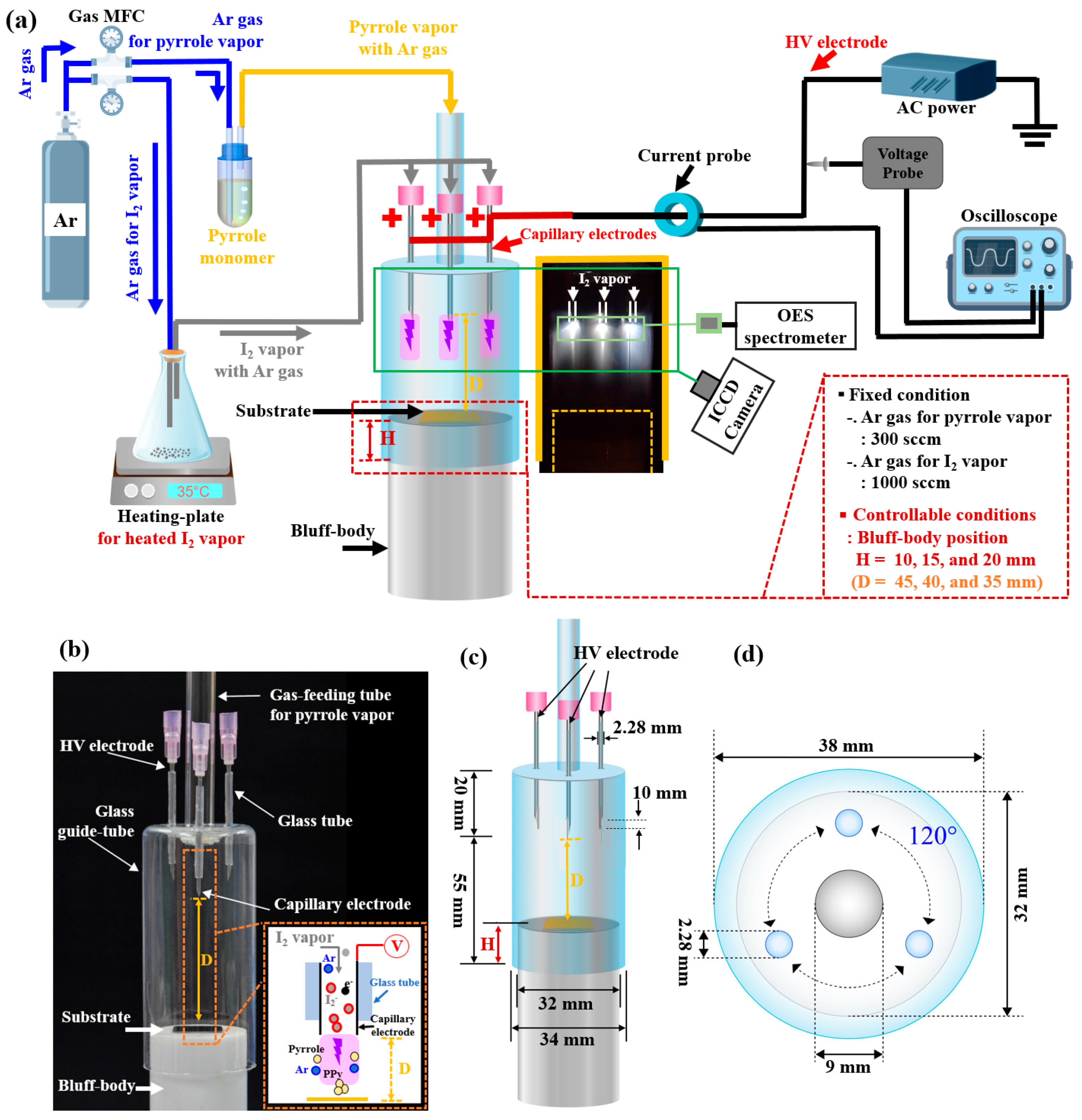
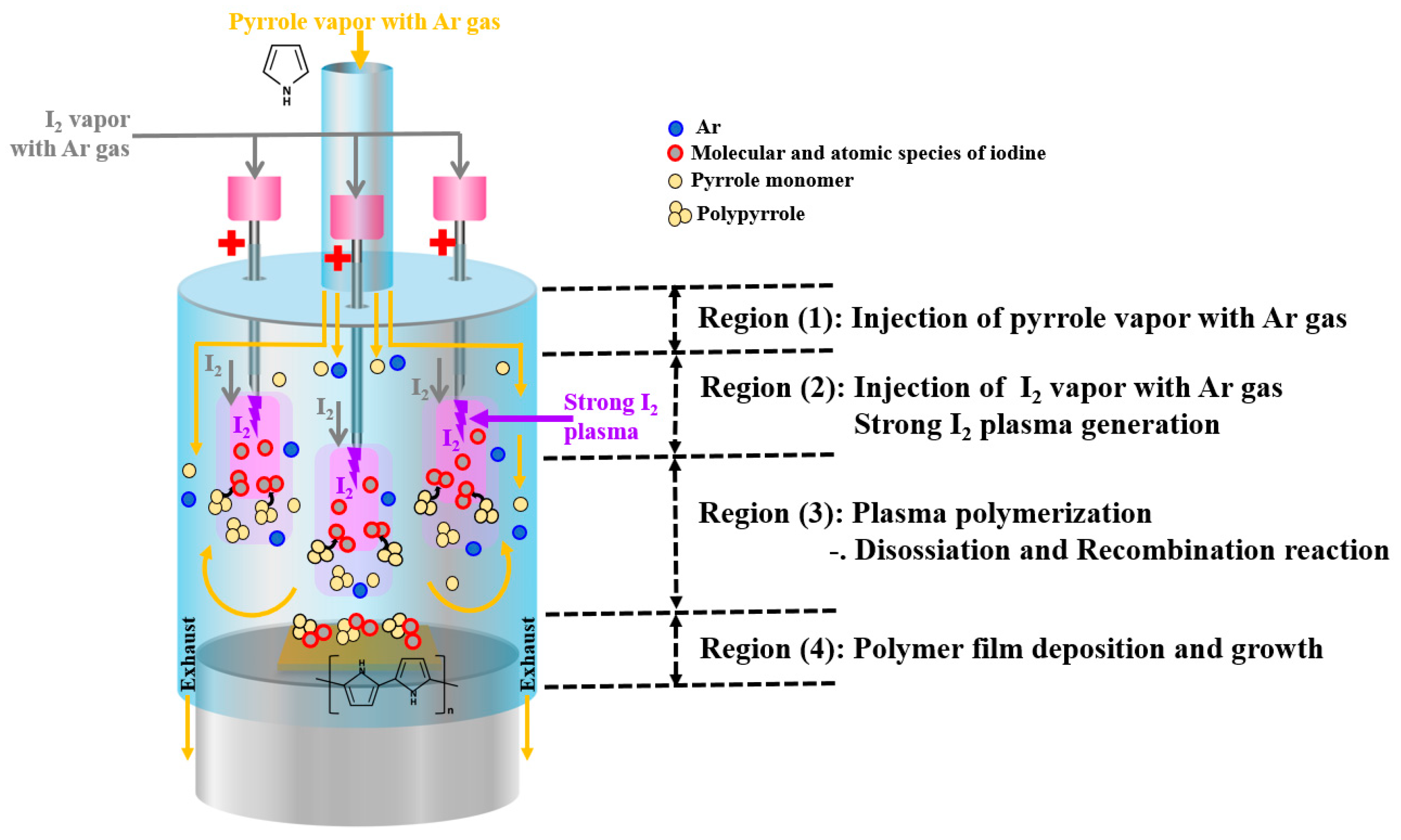
2.1. Experimental Setup
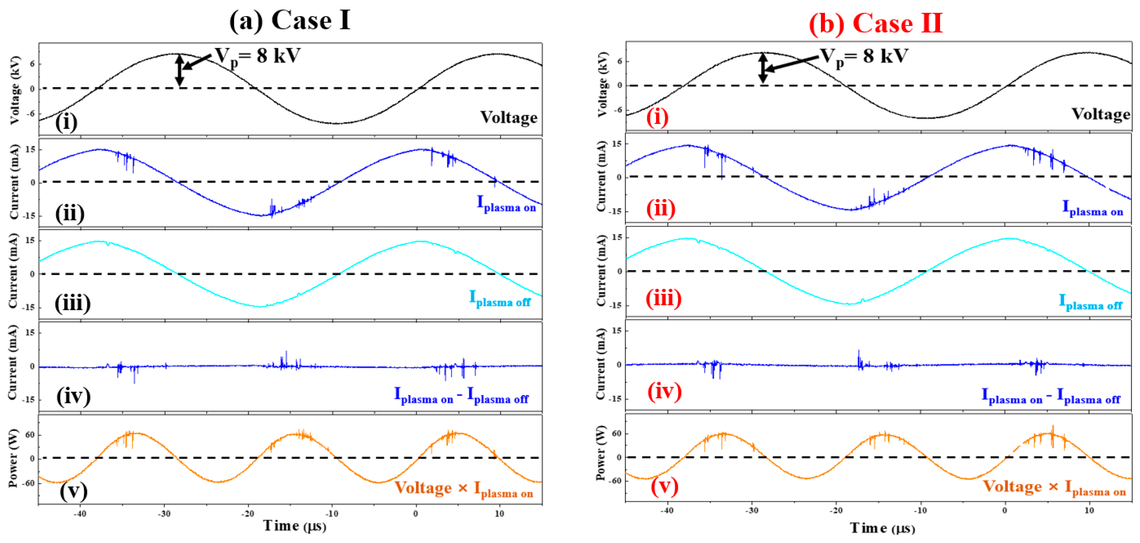
2.2. Discharge Voltage and Current Pulse Signal Analysis
2.3. ICCD and Digital Camera
2.4. OES
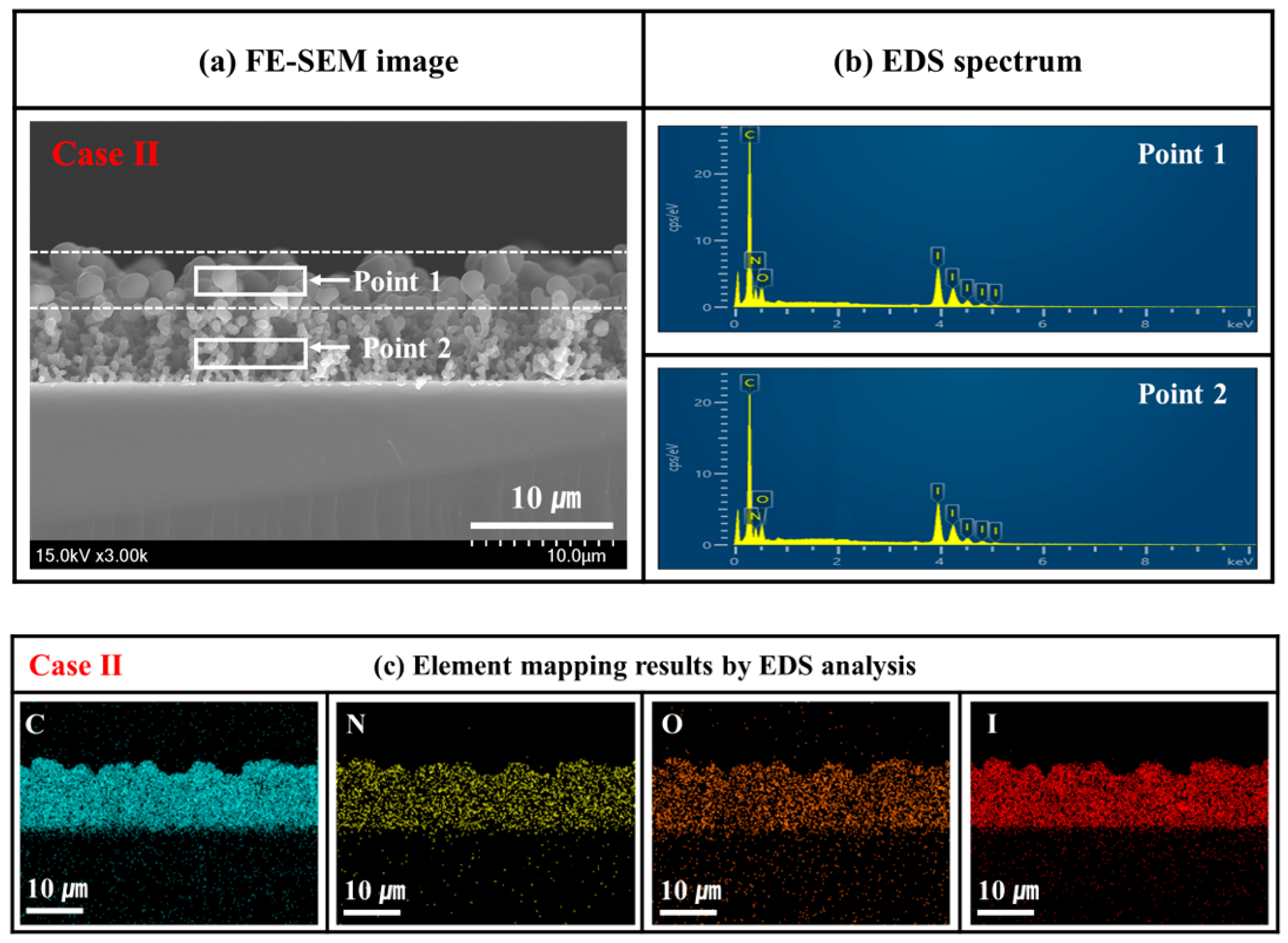
2.5. FE-SEM and EDX
2.6. FTIR Spectroscopy
2.7. Four-Point Probe
3. Results
3.1. Plasma Characterization
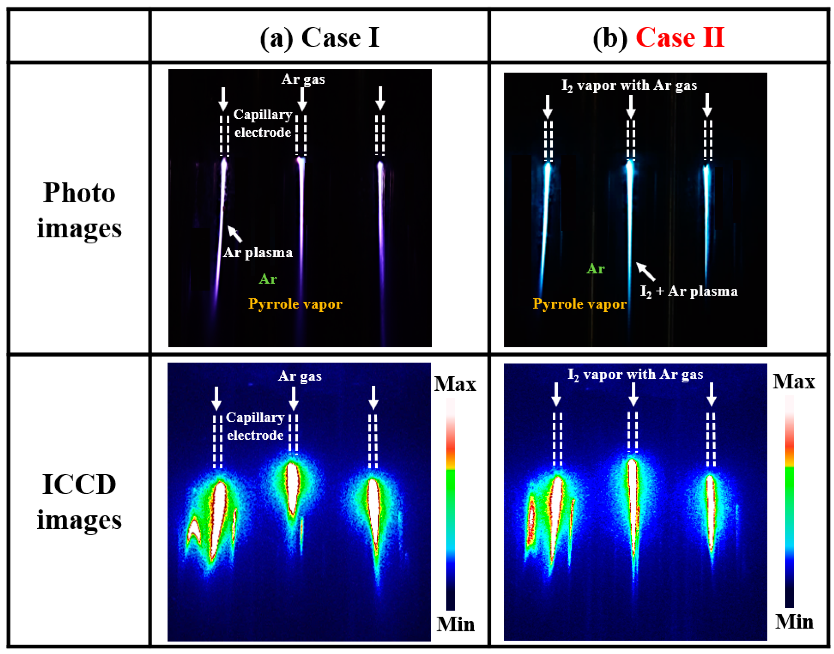
3.1.1. Photos and ICCD Images of the Produced Plasma Discharge
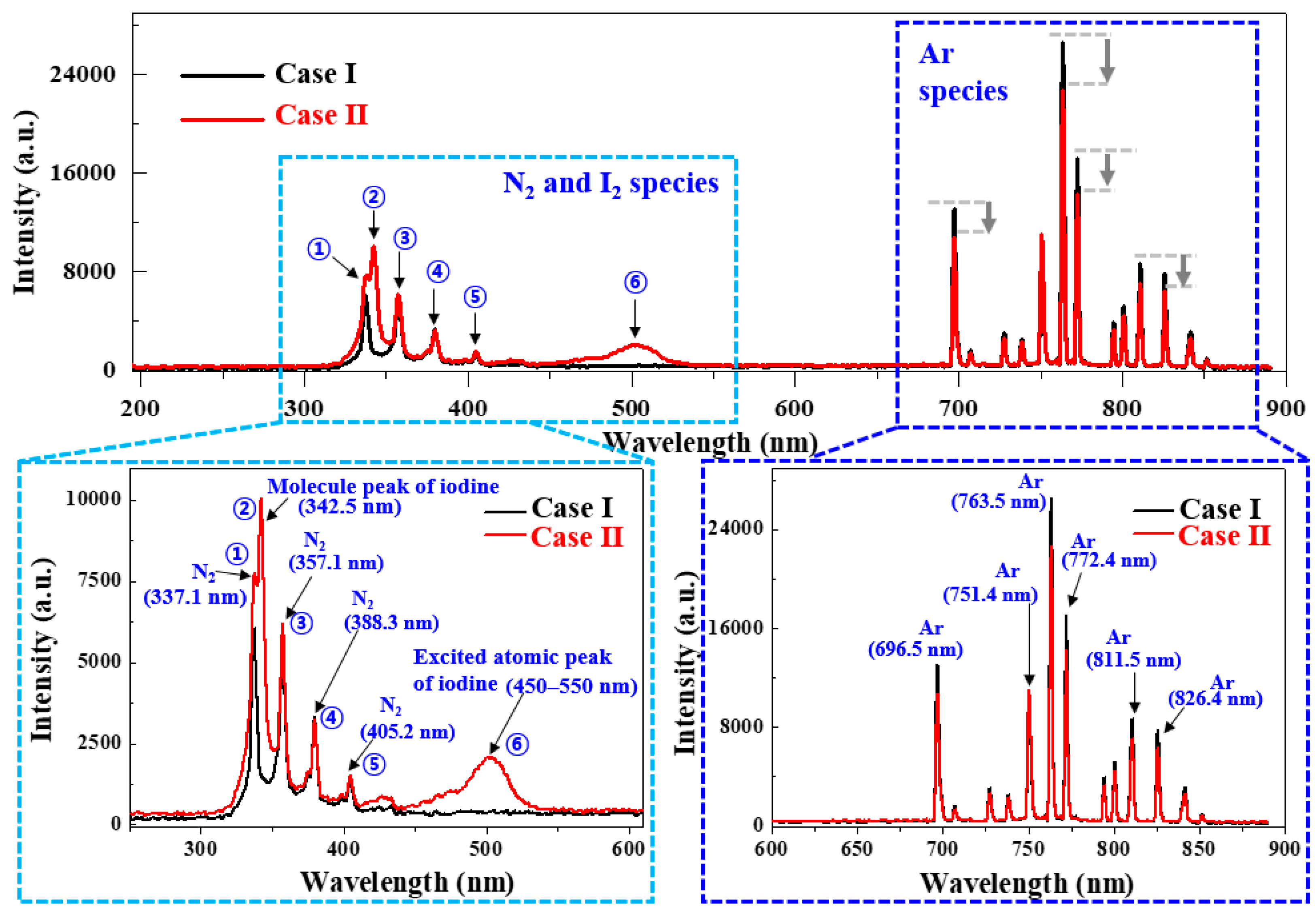
3.1.2. OES Results with Regard to the Produced Plasma Discharge
3.2. Characterization of the In Situ I2-Doped PPy Nanostructure Films
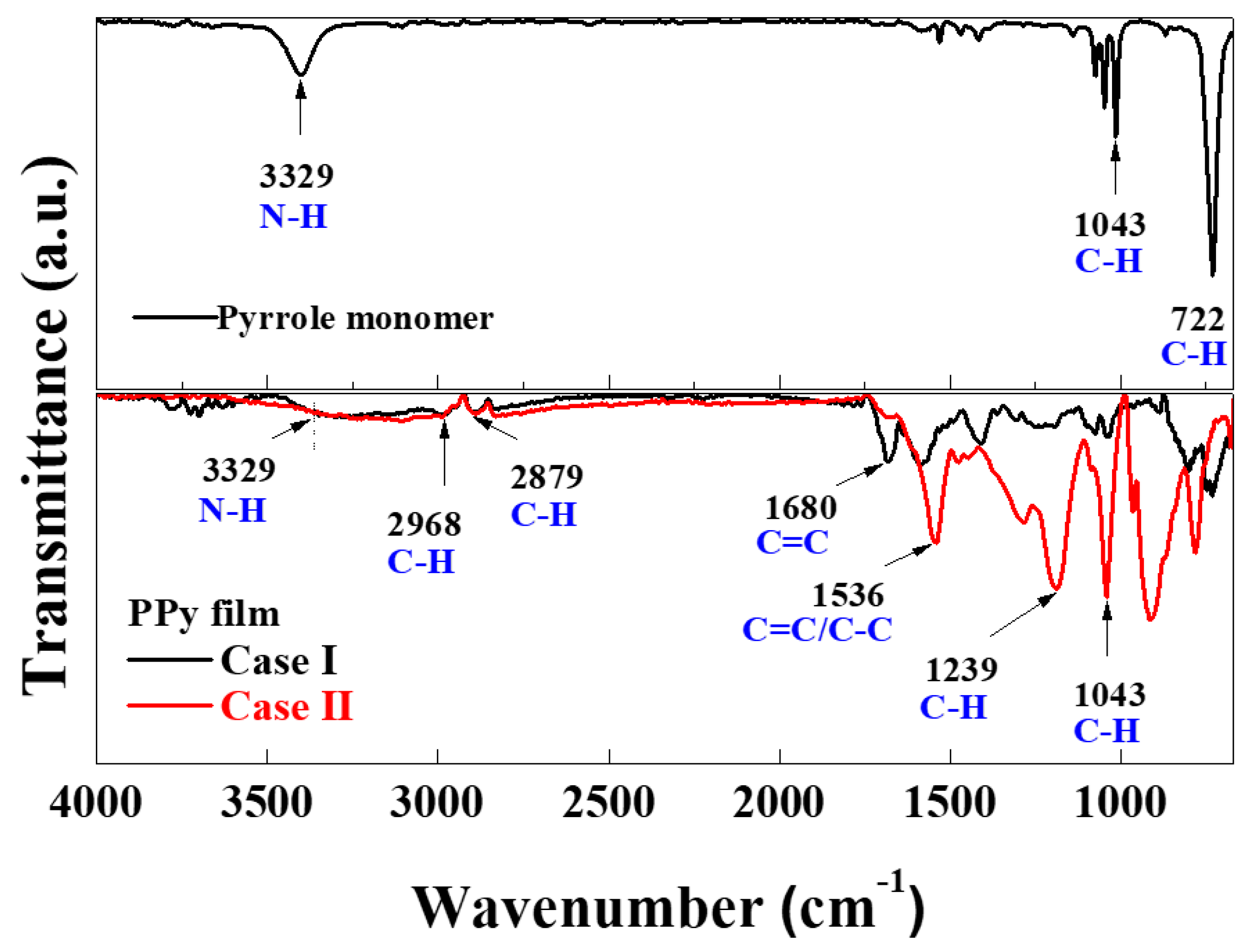
3.2.1. FTIR Spectra of the In Situ I2-Doped PPy Nanostructure Films
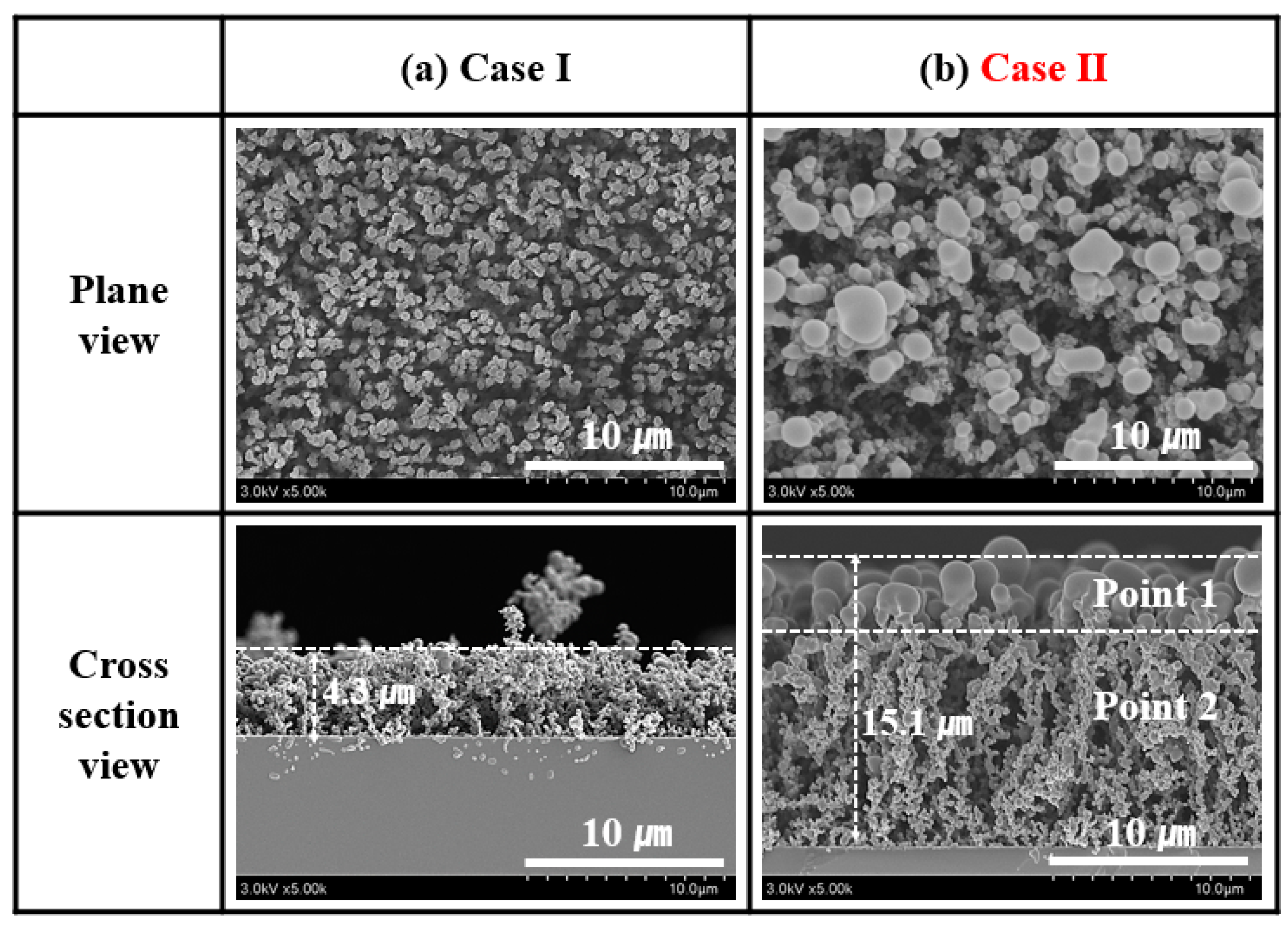
3.2.2. Plane-View and Cross-Section FE-SEM Images of the PPy Nanostructure Films
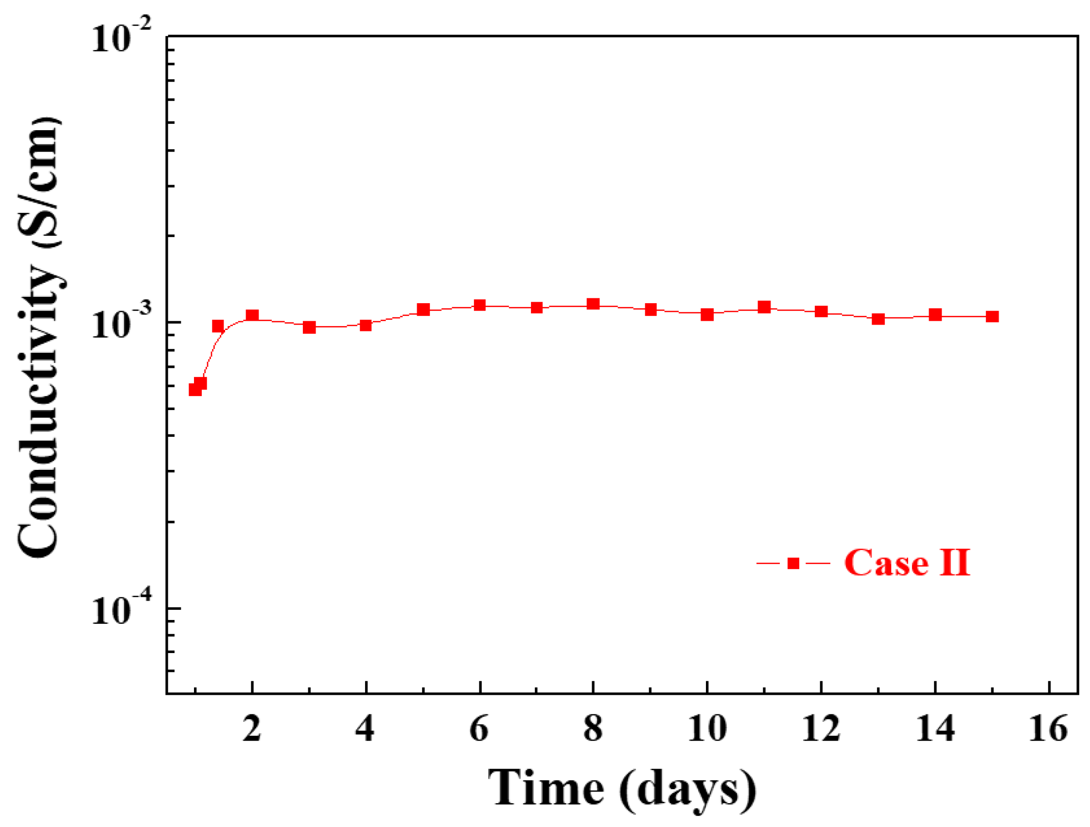
3.2.3. Electrical Conductivity of the In Situ I2-Doped Ppy Nanostructure Film
4. Conclusions
Author Contributions
Funding
Data Availability Statement
Conflicts of Interest
References
- Kaloni, T.P.; Schreckenbach, G.; Freund, M.S. Band gap modulation in polythiophene and polypyrrole-based systems. Sci. Rep. 2016, 6, 36554. [Google Scholar] [CrossRef]
- Elnaggar, E.M.; Kabel, K.I.; Farag, A.A.; Al-Gamal, A.G. Comparative study on doping of polyaniline with graphene and multi-walled carbon nanotubes. J. Nanostruct. Chem. 2017, 7, 75–83. [Google Scholar] [CrossRef]
- Dianatdar, A.; Miola, M.; Luca, O.D.; Rudolf, P.; Picchioni, F.; Bose, R.K. All-dry, one-step synthesis, doping and film formation of conductive polypyrrole. J. Mater. Chem. C 2022, 10, 557–570. [Google Scholar] [CrossRef]
- Zhang, J.; Xing, A.; Jia, B.; Liu, X. Synthesis of conductive polyaniline nanofibers in one step by protonic acid and iodine doping. High Perform. Polym. 2019, 31, 893–900. [Google Scholar] [CrossRef]
- Arbi, H.M.; Yadav, A.A.; Kumar, Y.A.; Moniruzzaman, M.; Alzahmi, S.; Obaidat, I.M. Polypyrrole-assisted Ag doping strategy to boost Co(OH)2 nanosheets on Ni foam as a novel electrode for high-performance hybrid supercapacitors. Nanomaterials 2022, 12, 3982. [Google Scholar] [CrossRef]
- Cruz-Reyes, E.D.; Hernández-Tenorio, C.; Villanueva-Castañeda, M.; Moreno-Saavedra, H.; Alejo-Eleuterio, R. Synthesis and characterization of polypyrrole thin films in a resistive plasma reactor by high frequency. MRS Adv. 2019, 4, 3311–3317. [Google Scholar] [CrossRef]
- Goto, H. Possibility for construction of an iodine cleaning system based on doping for π-conjugated polymers. Polymers 2011, 3, 875–885. [Google Scholar] [CrossRef]
- Li, M.; Luo, C.; Zhang, J.; Yang, J.; Xu, J.; Yao, W.; Tan, R.; Duan, X.; Jiang, F. Electrochemical doping tuning of flexible polypyrrole film with enhanced thermoelectric performance. Surf. Interfaces 2020, 21, 100759. [Google Scholar] [CrossRef]
- Chourasia, A.B.; Kelkar, D.S.; Chabukswar, V.V. Thermal conductivity of polythiophene doped with iodine. Res. J. Mater. Sci. 2016, 4, 1–5. [Google Scholar]
- Kamat, S.V.; Tamboli, S.H.; Puri, V.; Puri, R.K.; Yadav, J.B.; Joo, O.S. Optical and electrical properties of polythiophene thin films: Effect of post deposition heating. J. Optoelectron. Adv. Mater. 2010, 12, 2301–2305. [Google Scholar]
- Lee, H.O.; Sun, S.-S. Properties and mechanisms of iodine doped of P3HT and P3HT/PCBM composites. AIMS Mater. Sci. 2018, 5, 479–493. [Google Scholar]
- Mansuroglu, D.; Uzun-Kaymak, I.U. Investigation into ex-situ and in-situ iodine doped plasma polymerized fluorene-type thin films. Mater. Today Proc. 2019, 18, 1955–1963. [Google Scholar] [CrossRef]
- Humud, H.R.; Abdullah, M.M.; Khudhair, D.M. Effect of iodine doping on the characteristics of polythiophene thin films prepared by aerosol assisted plasma jet polymerization at atmospheric pressure. Iraqi J. Phys. 2014, 12, 127–137. [Google Scholar]
- Park, C.-S.; Kim, D.Y.; Kim, D.H.; Lee, H.-K.; Shin, B.J.; Tae, H.-S. Humidity-independent conducting polyaniline films synthesized using advanced atmospheric pressure plasma polymerization with in-situ iodine doping. Appl. Phys. Lett. 2017, 110, 033502. [Google Scholar] [CrossRef]
- Park, C.-S.; Jung, E.Y.; Kim, D.H.; Kim, D.Y.; Lee, H.-K.; Shin, B.J.; Lee, D.H.; Tae, H.-S. Atmospheric pressure plasma polymerization synthesis and characterization of polyaniline films doped with and without iodine. Materials 2017, 10, 1272. [Google Scholar] [CrossRef]
- Kim, J.Y.; Iqbal, S.; Jang, H.J.; Jung, E.Y.; Bae, G.T.; Park, C.-S.; Tae, H.-S. In-situ iodine doping characteristics of conductive polyaniline film polymerized by low-voltage-driven atmospheric pressure plasma. Polymers 2021, 13, 418. [Google Scholar] [CrossRef]
- Walter, C.; Brüser, V.; Quade, A.; Weltmann, K.-D. Structural investigations of composites produced from copper and polypyrrole with a dual PVD/PE-CVD process. Plasma Process Polym. 2009, 6, 803–812. [Google Scholar] [CrossRef]
- Yagüe, J.L.; Borrós, S. Conducting plasma polymerized polypyrrole thin films as carbon dioxide gas sensors. Plasma Process Polym. 2012, 9, 485–490. [Google Scholar] [CrossRef]
- Pattyn, C.; Sciacqua, D.; Kwiedor, L.; Jagodar, A.; Strunskus, T.; Traeger, F.; Lecas, T.; Kovacevic, E.; Berndt, J. Controlled deposition of plasma-polyaniline thin film by PECVD: Understanding the influence of aniline to argon ratio. Plasma Process Polym. 2022, 19, e2100233. [Google Scholar] [CrossRef]
- Cruz, G.J.; Morales, J.; Castillo-Ortega, M.M.; Olayo, R. Synthesis of polyaniline films by plasma polymerization. Synth. Met. 1997, 88, 213–218. [Google Scholar] [CrossRef]
- Cruz, G.J.; Morales, J.; Olayo, R. Films obtained by plasma polymerization of pyrrole. Thin Solid Film. 1999, 342, 119–126. [Google Scholar] [CrossRef]
- Paosawatyanyong, B.; Tapaneeyakorn, K.; Bhanthumnavin, W. AC plasma polymerization of pyrrole. Surf. Coat. Technol. 2010, 204, 3069–3072. [Google Scholar] [CrossRef]
- Humud, H.R.; Abdullah, M.M.; Khudhair, D.M. Nonlinear optical properties of polythiophene and iodine doped thin films by aerosol assisted plasma jet polymerization at atmospheric pressure. Int. J. Sci. Basic Appl. Res. (IJSBAR) 2017, 36, 70–80. [Google Scholar]
- Joseph Mathai, C.; Saravanan, S.; Anantharaman, M.R.; Venkitachalam, S.; Jayalekshmi, S. Characterization of low dielectric constant polyaniline thin film synthesized by ac plasma polymerization technique. J. Phys. D Appl. Phys. 2002, 35, 240–245. [Google Scholar] [CrossRef]
- Satulu, V.; Ion, V.; Aldica, G.; Mitu, B.; Dinescu, G. In-situ iodine doped polythiophene-like thin films obtained by post-discharge rf plasma. Rom. J. Phys. 2015, 60, 1550–1560. [Google Scholar]
- Shabeeb, G.M.; Abdullah, R.M.; Nazar, S. Effect of iodine doping on the polyaniline/clay nano composite thin films prepared by mechanochemical intercalation method. J. Nanostruc. 2022, 12, 1086–1096. [Google Scholar]
- Cruz, G.J.; Olayo, M.G.; López, O.G.; Gómez, L.M.; Morales, J.; Olayo, R. Nanospherical particles of polypyrrole synthesized and doped by plasma. Polymer 2010, 51, 4314–4318. [Google Scholar] [CrossRef]
- Yeon, J.-W.; Jung, S.-H. Effects of temperature and solution composition on evaporation of iodine as a part of estimating volatility of iodine under gamma irradiation. Nucl. Eng. Technol. 2017, 49, 1689–1695. [Google Scholar] [CrossRef]
- Habib, D.; Asmar, R.A.; Helou, Z.E.; Moussa, G.E.H. Influence of iodine pressure on the growth of CuIn1−xGaxSe2 thin films obtained by close-spaced vapor transport “CSVT”. World J. Condens. Matter Phys. 2013, 3, 164–168. [Google Scholar] [CrossRef]
- Szabo, J.; Robin, M.; Paintal, S.; Pote, B.; Hruby, V.; Freeman, C. Iodine propellant space propulsion. In Proceedings of the 33rd International Electric Propulsion Conference, Washington, DC, USA, 6–10 October 2013. [Google Scholar]
- Naftaly, M.; Das, S.; Gallop, J.; Pan, K.; Alkhalil, F.; Kariyapperuma, D.; Constant, S.; Ramsdale, C.; Hao, L. Sheet resistance measurements of conductive thin films: A comparison of techniques. Electronics 2021, 10, 960. [Google Scholar] [CrossRef]
- Zhang, J.; Wang, Y.; Wang, D. Computational simulation of atmospheric pressure discharges with the needle-array electrode. Phys. Plasmas 2018, 25, 072101. [Google Scholar] [CrossRef]
- Liu, T.; Timoshkin, I.; Wilson, M.P.; Given, M.J.; MacGregor, S.J. The nanosecond impulsive breakdown characteristics of air, N2, and CO2 in a sub-mm gap. Plasma 2022, 5, 12–29. [Google Scholar] [CrossRef]
- Liu, D.; Zhang, Z.; Liu, Z.; Wang, B.; Li, Q.; Wang, X.; Kong, M.G. Plasma jets with needle–ring electrodes: The insulated sealing of the needle and its effect on the plasma characteristics. IEEE Trans. Plasma Sci. 2018, 46, 2942–2948. [Google Scholar] [CrossRef]
- Sato, Y.; Ishikawa, K.; Tsutsumi, T.; Ui, A.; Akita, M.; Oka, S.; Hori, M. Numerical simulations of stable, high-electron-density atmospheric pressure argon plasma under pin-to-plane electrode geometry: Effects of applied voltage polarity. J. Phys. D Appl. Phys. 2020, 53, 265204. [Google Scholar] [CrossRef]
- Kim, D.H.; Park, C.-S.; Kim, W.H.; Shin, B.J.; Hong, J.G.; Park, T.S.; Seo, J.H.; Tae, H.-S. Influences of guide-tube and bluff-body on advanced atmospheric pressure plasma source for single-crystalline polymer nanoparticle synthesis at low temperature. Phys. Plasma 2017, 24, 023506. [Google Scholar] [CrossRef]
- Jung, E.Y.; Park, C.-S.; Jang, H.J.; Iqbal, S.; Hong, T.E.; Shin, B.J.; Choi, M.; Tae, H.-S. Optimization of atmospheric pressure plasma jet with single-pin electrode configuration and its application in polyaniline thin film growth. Polymers 2022, 14, 1535. [Google Scholar] [CrossRef]
- Lotfy, K. The impact of the carrier gas composition of non-thermal atmospheric pressure plasma jet for bacteria sterilization. AIP Adv. 2020, 10, 015303. [Google Scholar] [CrossRef]
- Xiao, D.; Cheng, C.; Lan, Y.; Ni, G.H.; Shen, J.; Meng, Y.D.; Chu, P.K. Effects of atmospheric pressure nonthermal nitrogen and air plasma on bacteria inactivation. IEEE Trans. Plasma Sci. 2016, 44, 2699–2707. [Google Scholar] [CrossRef]
- Mochalov, L.; Logunov, A.; Gogova, D.; Zelentsov, S.; Prokhorov, I.; Starostin, N.; Letnianchik, A.; Vorotyntsev, V. Synthesis of gallium oxide via interaction of gallium with iodide pentoxide in plasma. Opt. Quantum Electron. 2020, 52, 510. [Google Scholar] [CrossRef]
- Kim, J.Y.; Jang, H.J.; Jung, E.Y.; Bae, G.T.; Lee, S.W.; Park, C.-S.; Shin, B.J.; Tae, H.-S. Improvement of the uniformity and electrical properties of polyaniline nanocomposite film by addition of auxiliary gases during atmospheric pressure plasma polymerization. Nanomaterials 2021, 11, 2315. [Google Scholar] [CrossRef]
- Qayyum, A.; Zeb, S.; Naveed, M.A.; Rehman, N.U.; Ghauri, S.A.; Zakaullah, M. Optical emission spectroscopy of Ar–N2 mixture plasma. J. Quant. Spectrosc. Radiat. Transf. 2007, 107, 361–371. [Google Scholar] [CrossRef]
- Barkhordari, A.; Ganjovi, A.; Mirzaei, I.; Falahat, A.; Rostami Ravari, M.N. A pulsed plasma jet with the various Ar/N2 mixtures. J. Theor. Appl. Phys. 2017, 11, 301–312. [Google Scholar] [CrossRef]
- Kim, J.Y.; Jang, H.J.; Lee, Y.R.; Kim, K.M.; Suleiman, H.O.; Park, C.-S.; Shin, B.J.; Jung, E.Y.; Tae, H.-S. Nanostructured polyaniline films functionalized through auxiliary nitrogen addition in atmospheric pressure plasma polymerization. Polymers 2023, 15, 1626. [Google Scholar] [CrossRef]
- Kim, J.Y.; Sohn, D.W.; Sung, Y.Y.; Kim, E.-R. Fabrication and characterization of conductive polypyrrole thin film prepared by in situ vapor-phase polymerization. Synth. Met. 2003, 132, 309–313. [Google Scholar] [CrossRef]
- Wang, K.; Tan, H.; Lin, Y.; Diono, W.; Zhao, Y.; Goto, M. Direct current gas–liquid phase pulsed plasma polymerization of polypyrrole under atmospheric pressure. Plasma Process. Polym. 2021, 18, e2000186. [Google Scholar] [CrossRef]
- Dhillon, A.; Kaur, A.; Srivastava, A.K.; Avasthi, D.K. Experimental investigations of semi-crystalline plasma polymerized polypyrrole for surface coating. Prog. Org. Coat. 2010, 69, 396–401. [Google Scholar] [CrossRef]
- Izevbekhai, O.U.; Gitari, W.M.; Tavengwa, N.T.; Ayinde, W.B.; Mudzielwana, R. Response surface optimization of oil removal using synthesized polypyrrole-silica polymer composite. Molecules 2020, 25, 4628. [Google Scholar] [CrossRef]
- Novák, P.; Rasch, B.; Vielstich, W. Overoxidation of polypyrrole in propylene carbonate: An in situ FTIR study. J. Electrochem. Soc. 1991, 138, 3300–3304. [Google Scholar] [CrossRef]
- Wu, A.; Kolla, H.; Manohar, S.K. Chemical Synthesis of highly conducting polypyrrole nanofiber Film. Macromolecules 2005, 38, 7873–7875. [Google Scholar] [CrossRef]
- Hossein-Babaei, F.; Akbari, T.; Harkinezhad, B. Dopant passivation by adsorbed water monomers causes high humidity sensitivity in PEDOT: PSS thin films at ppm-level humidity. Sens. Actuators B Chem. 2019, 293, 329–335. [Google Scholar] [CrossRef]


| Electrode type | Three capillary electrodes |
| Precursor material | Pyrrole liquid monomer |
| Driving voltage waveform | AC sinusoidal |
| Driving voltage (Vp) | 8 kV |
| Frequency | 26 kHz |
| Ar gas flow for pyrrole vapor | 300 sccm |
| Ar gas flow for heated iodine vapor | 1000 sccm |
| Hot plate temperature for I2 vapor | 35 °C |
| Deposition time | 30 min |
| Bluff body height | H = 10, 15, and 20 mm (controllable) |
| Distance between electrode tip and substrate | D = 45, 40, and 35 mm (controllable) |
| Two cases of in situ I2 doping | Case I: no-doping |
| Case II: in situ I2 doping at 35 °C |
| Wave Number | Peak Assignment | |
|---|---|---|
| 722 cm−1 | C–H out of plane stretching | |
| Pyrrole monomer | 1043 cm−1 | C–H in-plane bend stretching |
| 3329 cm−1 | N–H stretching | |
| 1043 cm−1 | C–H in-plane-bend stretching | |
| 1239 cm−1 | C–N stretching | |
| 1536 cm−1 | C=C, C–C ring stretching | |
| PPy film | 1680 cm−1 | C=C stretching |
| 2879 cm−1 | C–H asymmetric stretching | |
| 2968 cm−1 | C–H symmetric stretching | |
| 3329 cm−1 | N–H stretching |
| Elemental Composition (Atomic %) | |||||
|---|---|---|---|---|---|
| C | N | O | I | Total | |
| Point 1 (top, big particle) | 69.9 | 20.1 | 4.8 | 5.2 | 100 |
| Point 2 (inner, small particle) | 69.0 | 19.6 | 5.7 | 5.7 | 100 |
| Heating Temperature (°C) | I2 Weight (g) | I2 Weight (g) Used for Process | |
|---|---|---|---|
| Before | After 30 min | ||
| Room temperature | 10 | 9.9 | 0.1 |
| 35 | 10 | 9.8 | 0.2 |
| 50 | 10 | 9.7 | 0.3 |
Disclaimer/Publisher’s Note: The statements, opinions and data contained in all publications are solely those of the individual author(s) and contributor(s) and not of MDPI and/or the editor(s). MDPI and/or the editor(s) disclaim responsibility for any injury to people or property resulting from any ideas, methods, instructions or products referred to in the content. |
© 2024 by the authors. Licensee MDPI, Basel, Switzerland. This article is an open access article distributed under the terms and conditions of the Creative Commons Attribution (CC BY) license (https://creativecommons.org/licenses/by/4.0/).
Share and Cite
Jung, E.Y.; Khalil, S.; Jang, H.; Suleiman, H.O.; Kim, J.Y.; Shin, B.J.; Tae, H.-S.; Park, C.-S. Improvement of Electrical Conductivity of In Situ Iodine-Doped Polypyrrole Film Using Atmospheric Pressure Plasma Reactor with Capillary Electrodes. Nanomaterials 2024, 14, 468. https://doi.org/10.3390/nano14050468
Jung EY, Khalil S, Jang H, Suleiman HO, Kim JY, Shin BJ, Tae H-S, Park C-S. Improvement of Electrical Conductivity of In Situ Iodine-Doped Polypyrrole Film Using Atmospheric Pressure Plasma Reactor with Capillary Electrodes. Nanomaterials. 2024; 14(5):468. https://doi.org/10.3390/nano14050468
Chicago/Turabian StyleJung, Eun Young, Salman Khalil, Hyojun Jang, Habeeb Olaitan Suleiman, Jae Young Kim, Bhum Jae Shin, Heung-Sik Tae, and Choon-Sang Park. 2024. "Improvement of Electrical Conductivity of In Situ Iodine-Doped Polypyrrole Film Using Atmospheric Pressure Plasma Reactor with Capillary Electrodes" Nanomaterials 14, no. 5: 468. https://doi.org/10.3390/nano14050468