
Fast-Growth Polymer: Fullerene Bulk-Heterojunction Thin Films for Efficient Organic Photovoltaics
 , , and
Abstract
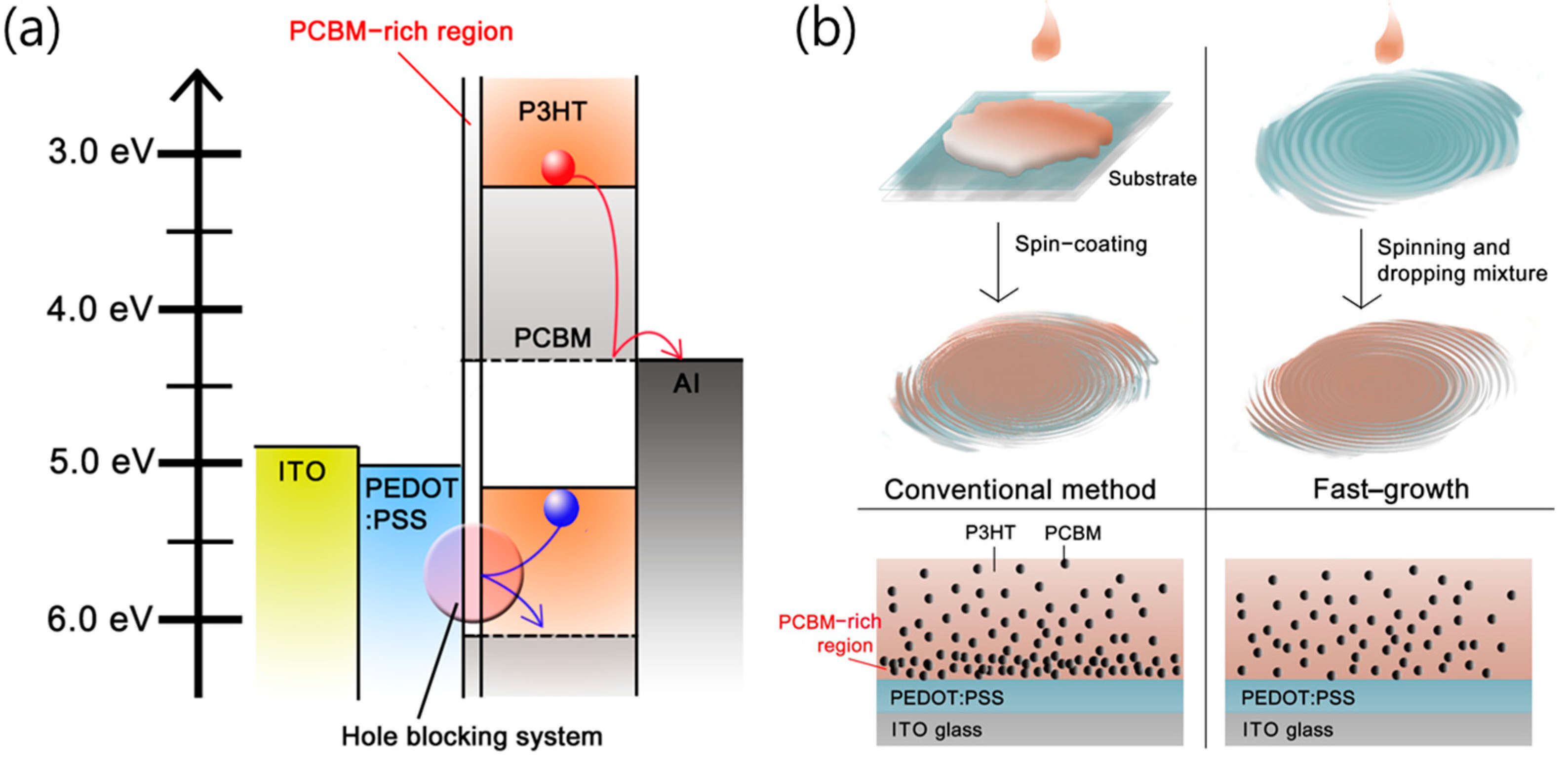
:1. Introduction
2. Materials and Methods
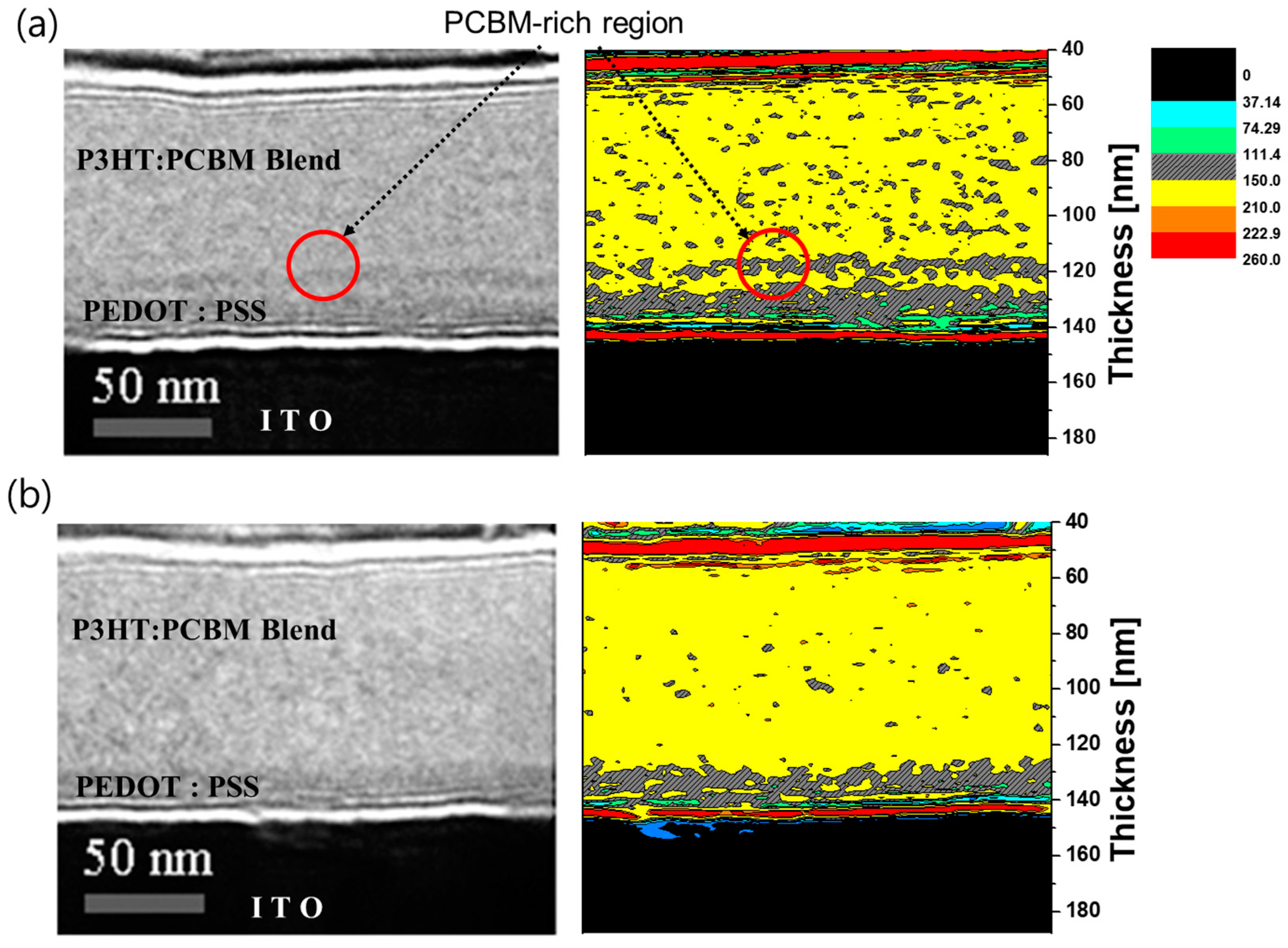
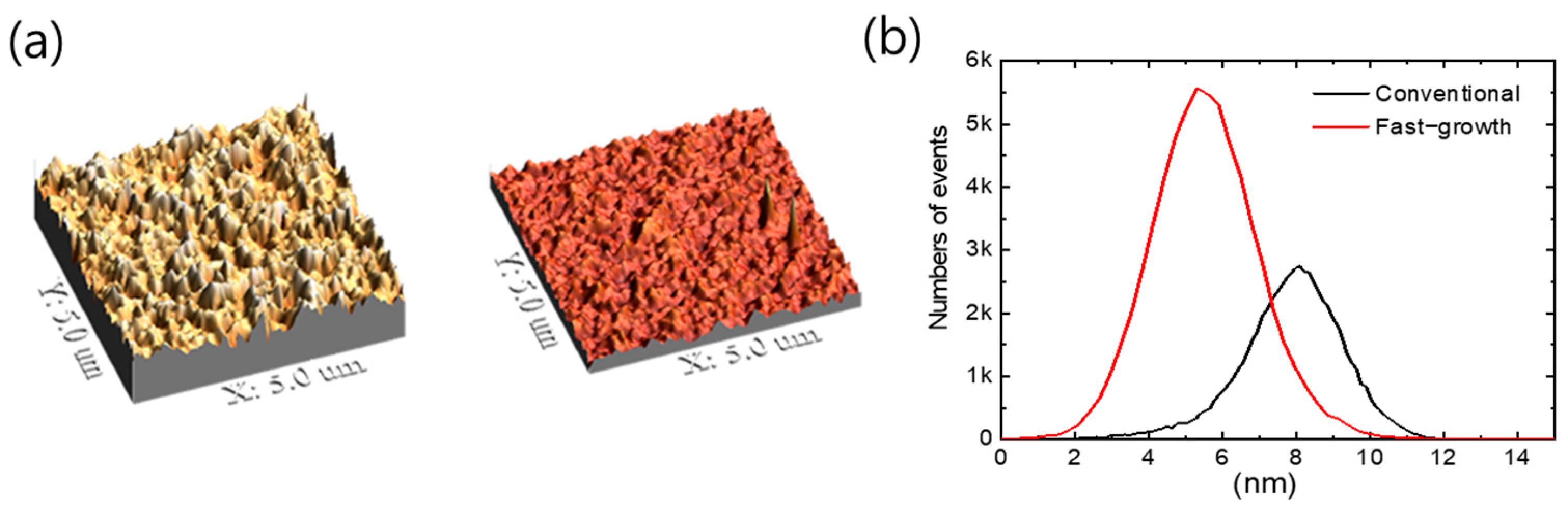
3. Results and Discussions
4. Conclusions
Supplementary Materials
Author Contributions
Funding
Data Availability Statement
Conflicts of Interest
References
- Sariciftci, N.S.; Smilowitz, L.; Heeger, A.J.; Wudl, F. Photoinduced Electron Transfer from a Conducting Polymer to Buckminsterfullerene. Science 1992, 258, 1474–1476. [Google Scholar] [CrossRef] [PubMed]
- Fukuda, K.; Yu, K.; Someya, T. The Future of Flexible Organic Solar Cells. Adv. Energy Mater. 2020, 10, 2000765. [Google Scholar] [CrossRef]
- Duan, L.; Uddin, A. Progress in Stability of Organic Solar Cells. Adv. Sci. 2020, 7, 1903259. [Google Scholar] [CrossRef] [PubMed]
- Yao, H.; Hou, J. Recent Advances in Single-Junction Organic Solar Cells. Angew. Chem. 2022, 134, e202209021. [Google Scholar] [CrossRef]
- Wei, Y.; Chen, Z.; Lu, G.; Yu, N.; Li, C.; Gao, J.; Gu, X.; Hao, X.; Lu, G.; Tang, Z.; et al. Binary Organic Solar Cells Breaking 19% via Manipulating the Vertical Component Distribution. Adv. Mater. 2022, 34, 2204718. [Google Scholar] [CrossRef] [PubMed]
- Zhu, L.; Zhang, M.; Xu, J.; Li, C.; Yan, J.; Zhou, G.; Zhong, W.; Hao, T.; Song, J.; Xue, X.; et al. Single-junction organic solar cells with over 19% efficiency enabled by a refined double-fibril network morphology. Nat. Mater. 2022, 21, 656–663. [Google Scholar] [CrossRef]
- Gao, W.; Qi, F.; Peng, Z.; Lin, F.R.; Jiang, K.; Zhong, C.; Kaminsky, W.; Guan, Z.; Lee, C.-S.; Marks, T.J.; et al. Achieving 19% Power Conversion Efficiency in Planar-Mixed Heterojunction Organic Solar Cells Using a Pseudosymmetric Electron Acceptor. Adv. Mater. 2022, 34, 2202089. [Google Scholar] [CrossRef]
- Chen, W.; Xu, T.; He, F.; Wang, W.; Wang, C.; Strzalka, J.; Liu, Y.; Wen, J.; Miller, D.J.; Chen, J.; et al. Hierarchical Nanomorphologies Promote Exciton Dissociation in Polymer/Fullerene Bulk Heterojunction Solar Cells. Nano Lett. 2011, 11, 3707–3713. [Google Scholar] [CrossRef]
- Yoshimoto, Y.; Sugiyama, S.; Shimada, S.; Kaneko, T.; Takagi, S.; Kinefuchi, I. Molecular Insights into the Mechanical Properties of Polymer–Fullerene Bulk Heterojunctions for Organic Photovoltaic Applications. Macromolecules 2021, 54, 958–969. [Google Scholar] [CrossRef]
- Levitsky, A.; Schneider, S.A.; Rabkin, E.; Toney, M.F.; Frey, G.L. Bridging the thermodynamics and kinetics of temperature-induced morphology evolution in polymer/fullerene organic solar cell bulk heterojunction. Mater. Horiz. 2021, 8, 1272–1285. [Google Scholar] [CrossRef]
- Carsten, B.; Szarko, J.M.; Son, H.J.; Wang, W.; Lu, L.; He, F.; Rolczynski, B.S.; Lou, S.J.; Chen, L.X.; Yu, L. Examining the Effect of the Dipole Moment on Charge Separation in Donor–Acceptor Polymers for Organic Photovoltaic Applications. J. Am. Chem. Soc. 2011, 133, 20468–20475. [Google Scholar] [CrossRef] [PubMed]
- Chen, W.; Nikiforov, M.P.; Darling, S.B. Morphology Characterization in Organic and Hybrid Solar Cells. Energy Environ. Sci. 2012, 5, 8045–8074. [Google Scholar] [CrossRef]
- Yan, H.; Tang, Y.; Sui, X.; Liu, Y.; Gao, B.; Liu, X.; Liu, S.F.; Hou, J.; Ma, W. Increasing Quantum Efficiency of Polymer Solar Cells with Efficient Exciton Splitting and Long Carrier Lifetime by Molecular Doping at Heterojunctions. ACS Energy Lett. 2019, 4, 1356–1363. [Google Scholar] [CrossRef]
- Lin, Y.; Nugraha, M.I.; Firdaus, Y.; Scaccabarozzi, A.D.; Aniés, F.; Emwas, A.-H.; Yengel, E.; Zheng, X.; Liu, J.; Wahyudi, W.; et al. A Simple n-Dopant Derived from Diquat Boosts the Efficiency of Organic Solar Cells to 18.3%. ACS Energy Lett. 2020, 5, 3663–3671. [Google Scholar] [CrossRef]
- Li, D.; Geng, F.; Hao, T.; Chen, Z.; Wu, H.; Ma, Z.; Xue, Q.; Lin, L.; Huang, R.; Leng, S.; et al. n-Doping of Photoactive Layer in Binary Organic Solar Cells Realizes over 18.3% Efficiency. Nano Energy 2022, 96, 107133. [Google Scholar] [CrossRef]
- Zhao, F.; Wang, C.; Zhan, X. Morphology Control in Organic Solar Cells. Adv. Energy Mater. 2018, 8, 1703147. [Google Scholar] [CrossRef]
- Liu, J.; Liu, X.; Xin, J.; Zhang, Y.; Wen, L.; Liang, Q.; Miao, Z. Dual Function of the Third Component in Ternary Organic Solar Cells: Broaden the Spectrum and Optimize the Morphology. Small 2024, 2308863. [Google Scholar] [CrossRef]
- Liao, S.-H.; Jhuo, H.-J.; Cheng, Y.-S.; Chen, S.-A. Fullerene Derivative-Doped Zinc Oxide Nanofilm as the Cathode of Inverted Polymer Solar Cells with Low-Bandgap Polymer (PTB7-Th) for High Performance. Adv. Mater. 2013, 25, 4766–4771. [Google Scholar] [CrossRef]
- Zhang, M.; Guo, X.; Ma, W.; Ade, H.; Hou, J. A Large-Bandgap Conjugated Polymer for Versatile Photovoltaic Applications with High Performance. Adv. Mater. 2015, 27, 4655–4660. [Google Scholar] [CrossRef]
- Yuan, J.; Zhang, Y.; Zhou, L.; Zhang, G.; Yip, H.-L.; Lau, T.-K.; Lu, X.; Zhu, C.; Peng, H.; Johnson, P.A.; et al. Single-Junction Organic Solar Cell with over15% Efficiency Using Fused-Ring Acceptor with Electron-Deficient Core. Joule 2019, 3, 1140–1151. [Google Scholar] [CrossRef]
- Song, J.; Zhu, L.; Li, C.; Xu, J.; Wu, H.; Zhang, X.; Zhang, Y.; Tang, Z.; Liu, F.; Sun, Y. High-Efficiency Organic Solar Cells with Low Voltage Loss Induced by Solvent Additive Strategy. Matter 2021, 4, 2542–2552. [Google Scholar] [CrossRef]
- Ma, Y.-F.; Zhang, Y.; Zhang, H.-L. Solid Additives in Organic Solar Cells: Progress and Perspectives. J. Mater. Chem. C 2022, 10, 2364–2374. [Google Scholar] [CrossRef]
- Ware, W.; Wright, T.; Mao, Y.; Han, S.; Guffie, J.; Danilov, E.O.; Rech, J.; You, W.; Luo, Z.; Gautam, B. Aggregation Controlled Charge Generation in Fullerene Based Bulk Heterojunction Polymer Solar Cells: Effect of Additive. Polymers 2021, 13, 115. [Google Scholar] [CrossRef] [PubMed]
- Distler, A.; Cheon, K.-S.; Waller, D.; Guldi, D.; Hauch, J.; Egelhaaf, H.-J. Influence of the Fullerene LUMO Level on the Stability of Bulk Heterojunction Solar Cells. J. Mater. Chem. C 2021, 9, 9271–9281. [Google Scholar] [CrossRef]
- Radaoui, M.; Fredj, A.B.; Romdhane, S.; Egbe, D.A.M.; Bouchriha, H. Annealing Temperature Dependence of the Performance of Bulk Heterojunction Polymer:Fullerene Solar Cells under Short and Open Circuit Conditions. Synth. Met. 2021, 271, 116611. [Google Scholar] [CrossRef]
- Wang, Y.; Shi, Z.; Liu, H.; Wang, F.; Bai, Y.; Bian, X.; Zhang, B.; Hayat, T.; Alsaedi, A.; Tan, Z. The Effect of Donor and Nonfullerene Acceptor Inhomogeneous Distribution within the Photoactive Layer on the Performance of Polymer Solar Cells with Different Device Structures. Polymers 2017, 9, 571. [Google Scholar] [CrossRef]
- Müller, C.; Ferenczi, T.A.M.; Campoy-Quiles, M.; Frost, J.M.; Bradley, D.D.C.; Smith, P.; Stingelin-Stutzmann, N.; Nelson, J. Binary Organic Photovoltaic Blends: A Simple Rationale for Optimum Compositions. Adv. Mater. 2008, 20, 3510–3515. [Google Scholar] [CrossRef]
- Baek, W.-H.; Yoon, T.-S.; Lee, H.H.; Kim, Y.-S. Composition-Dependent Phase Separation of P3HT: PCBM Composites for High Performance Organic Solar Cells. Org. Electron. 2010, 11, 933–937. [Google Scholar] [CrossRef]
- Bartesaghi, D.; Pérez, I.D.C.; Kniepert, J.; Roland, S.; Turbiez, M.; Neher, D.; Koster, L.J.A. Competition between Recombination and Extraction of Free Charges Determines the Fill Factor of Organic Solar Cells. Nat. Commun. 2015, 6, 7083. [Google Scholar] [CrossRef]
- Benten, H.; Mori, D.; Ohkita, H.; Ito, S. Recent Research Progress of Polymer Donor/Polymer Acceptor Blend Solar Cells. J. Mater. Chem. A 2016, 4, 5340–5365. [Google Scholar] [CrossRef]
- Liu, X.; Zou, Y.; Wang, H.-Q.; Wang, L.; Fang, J.; Yang, C. High-Performance All-Polymer Solar Cells with a High Fill Factor and a Broad Tolerance to the Donor/Acceptor Ratio. ACS Appl. Mater. Interfaces 2018, 10, 38302–38309. [Google Scholar] [CrossRef] [PubMed]
- Woo, C.H.; Beaujuge, P.M.; Holcombe, T.W.; Lee, O.P.; Fréchet, J.M.J. Incorporation of Furan into Low Band-Gap Polymers for Efficient Solar Cells. J. Am. Chem. Soc. 2010, 132, 15547–15549. [Google Scholar] [CrossRef] [PubMed]
- Zheng, Z.; Hu, Q.; Zhang, S.; Zhang, D.; Wang, J.; Xie, S.; Wang, R.; Qin, Y.; Li, W.; Hong, L.; et al. A Highly Efficient Non-Fullerene Organic Solar Cell with a Fill Factor over 0.80 Enabled by a Fine-Tuned Hole-Transporting Layer. Adv. Mater. 2018, 30, 1801801. [Google Scholar] [CrossRef] [PubMed]
- Wang, J.; Zheng, Z.; Zhang, D.; Zhang, J.; Zhou, J.; Liu, J.; Xie, S.; Zhao, Y.; Zhang, Y.; Wei, Z.; et al. Regulating Bulk-Heterojunction Molecular Orientations through Surface Free Energy Control of Hole-Transporting Layers for High-Performance Organic Solar Cells. Adv. Mater. 2019, 31, 1806921. [Google Scholar] [CrossRef] [PubMed]
- Björström, C.M.; Bernasik, A.; Rysz, J.; Budkowski, A.; Nilsson, S.; Svensson, M.; Andersson, M.R.; Magnusson, K.O.; Moons, E. Multilayer Formation in Spin-Coated Thin Films of Low-Bandgap Polyfluorene:PCBM Blends. J. Phys. Condens. Matter 2005, 17, L529. [Google Scholar] [CrossRef]
- Wang, X.; Ederth, T.; Inganäs, O. In Situ Wilhelmy Balance Surface Energy Determination of Poly(3-Hexylthiophene) and Poly(3,4-Ethylenedioxythiophene) during Electrochemical Doping−Dedoping. Langmuir 2006, 22, 9287–9294. [Google Scholar] [CrossRef]
- Björström, C.M.; Nilsson, S.; Bernasik, A.; Budkowski, A.; Andersson, M.; Magnusson, K.O.; Moons, E. Vertical Phase Separation in Spin-Coated Films of a Low Bandgap Polyfluorene/PCBM Blend–Effects of Specific Substrate Interaction. Appl. Surf. Sci. 2007, 253, 3906–3912. [Google Scholar] [CrossRef]
- Xu, Z.; Chen, L.; Yang, G.; Huang, C.; Hou, J.; Wu, Y.; Li, G.; Hsu, C.; Yang, Y. Vertical Phase Separation in Poly(3-hexylthiophene): Fullerene Derivative Blends and Its Advantage for Inverted Structure Solar Cells. Adv. Funct. Mater. 2009, 19, 1227–1234. [Google Scholar] [CrossRef]
- Oklobia, O.; Shafai, T.S. A Quantitative Study of the Formation of PCBM Clusters upon Thermal Annealing of P3HT/PCBM Bulk Heterojunction Solar Cell. Sol. Energy Mat. Sol. Cells 2013, 117, 1–8. [Google Scholar] [CrossRef]
- Bartelt, J.A.; Beiley, Z.M.; Hoke, E.T.; Mateker, W.R.; Douglas, J.D.; Collins, B.A.; Tumbleston, J.R.; Graham, K.R.; Amassian, A.; Ade, H.; et al. The Importance of Fullerene Percolation in the Mixed Regions of Polymer–Fullerene Bulk Heterojunction Solar Cells. Adv. Energy Mater. 2013, 3, 364–374. [Google Scholar] [CrossRef]
- Kim, J.; Kim, G.; Back, H.; Kong, J.; Hwang, I.; Kim, T.K.; Kwon, S.; Lee, J.; Lee, J.; Yu, K.; et al. High-Performance Integrated Perovskite and Organic Solar Cells with Enhanced Fill Factors and Near-Infrared Harvesting. Adv. Mater. 2016, 28, 3159–3165. [Google Scholar] [CrossRef] [PubMed]
- Lin, K.; Xing, J.; Quan, L.N.; de Arquer, F.P.G.; Gong, X.; Lu, J.; Xie, L.; Zhao, W.; Zhang, D.; Yan, C. Perovskite Light-Emitting Diodes with External Quantum Efficiency Exceeding 20 per Cent. Nature 2018, 562, 245–248. [Google Scholar] [CrossRef] [PubMed]
- Slooff, L.H.; Veenstra, S.C.; Kroon, J.M.; Moet, D.J.D.; Sweelssen, J.; Koetse, M.M. Determining the Internal Quantum Efficiency of Highly Efficient Polymer Solar Cells through Optical Modeling. Appl. Phys. Lett. 2007, 90, 143506. [Google Scholar] [CrossRef]
- Liang, Y.; Yu, L. A New Class of Semiconducting Polymers for Bulk Heterojunction Solar Cells with Exceptionally High Performance. Acc. Chem. Res. 2010, 43, 1227–1236. [Google Scholar] [CrossRef]


| JSC (mA/cm2) | VOC (V) | FF | PCE (%) | |
|---|---|---|---|---|
| Conventional | 10.3 | 0.63 | 0.60 | 3.88 |
| Fast-growth | 11.3 | 0.63 | 0.66 | 4.68 |
| JSC (mA/cm2) | VOC (V) | FF | PCE (%) | |
|---|---|---|---|---|
| Conventional | 25.4 | 0.84 | 0.70 | 14.8 |
| Fast growth | 26.0 | 0.84 | 0.72 | 15.7 |
Disclaimer/Publisher’s Note: The statements, opinions and data contained in all publications are solely those of the individual author(s) and contributor(s) and not of MDPI and/or the editor(s). MDPI and/or the editor(s) disclaim responsibility for any injury to people or property resulting from any ideas, methods, instructions or products referred to in the content. |
© 2024 by the authors. Licensee MDPI, Basel, Switzerland. This article is an open access article distributed under the terms and conditions of the Creative Commons Attribution (CC BY) license (https://creativecommons.org/licenses/by/4.0/).
Share and Cite
Chung, D.; Balamurugan, C.; Park, B.; Lee, H.; Cho, I.; Yoon, C.; Park, S.; Jo, Y.-R.; Jeon, J.; Hong, S.; et al. Fast-Growth Polymer: Fullerene Bulk-Heterojunction Thin Films for Efficient Organic Photovoltaics. Nanomaterials 2024, 14, 502. https://doi.org/10.3390/nano14060502
Chung D, Balamurugan C, Park B, Lee H, Cho I, Yoon C, Park S, Jo Y-R, Jeon J, Hong S, et al. Fast-Growth Polymer: Fullerene Bulk-Heterojunction Thin Films for Efficient Organic Photovoltaics. Nanomaterials. 2024; 14(6):502. https://doi.org/10.3390/nano14060502
Chicago/Turabian StyleChung, Daewon, Chandran Balamurugan, Byoungwook Park, Hyeonryul Lee, Ilhyeon Cho, Chaerin Yoon, Soyeon Park, Yong-Ryun Jo, Joonhyeon Jeon, Soonil Hong, and et al. 2024. "Fast-Growth Polymer: Fullerene Bulk-Heterojunction Thin Films for Efficient Organic Photovoltaics" Nanomaterials 14, no. 6: 502. https://doi.org/10.3390/nano14060502