
A Microfabrication Technique for High-Performance Diffractive Optical Elements Tailored for Numerical Simulation

 ,
,
Abstract
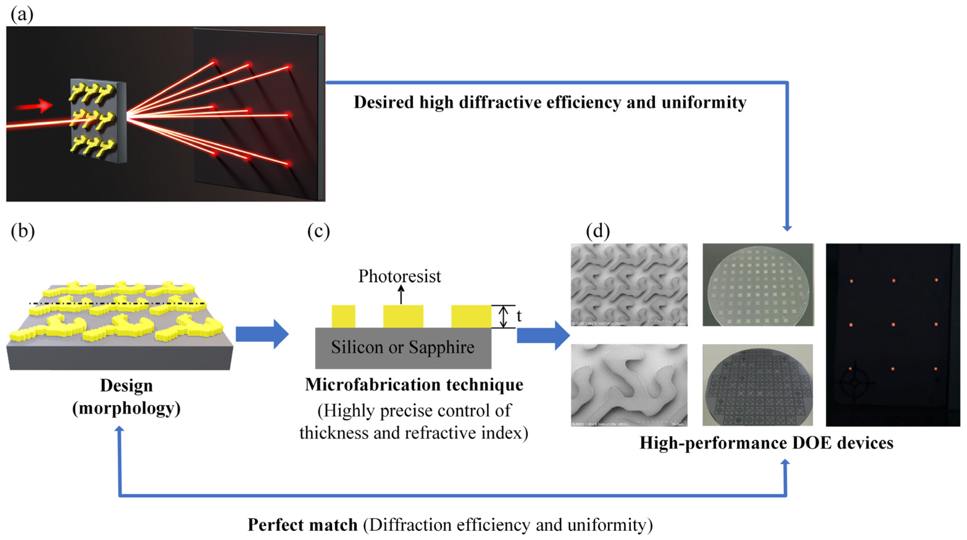
1. Introduction
2. Materials and Methods
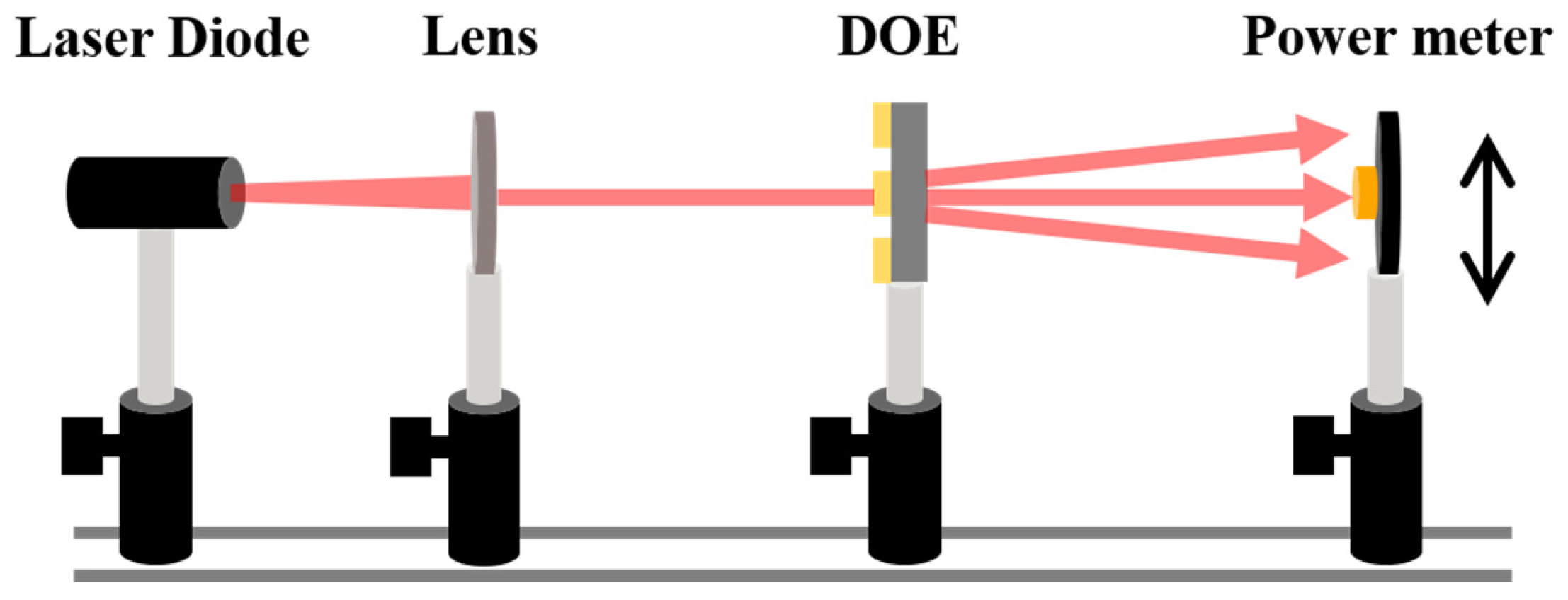
2.1. Optical Performance Evaluation
2.2. Material Selection of DOE
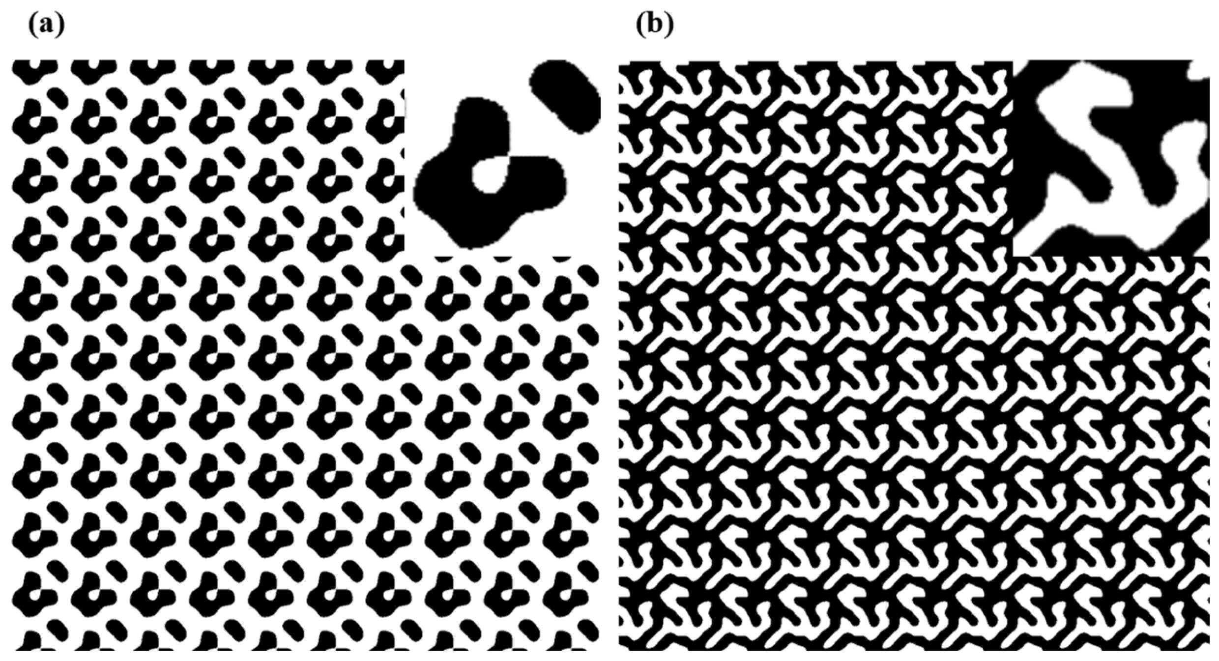
2.3. Periodic Diffractive Structure Design
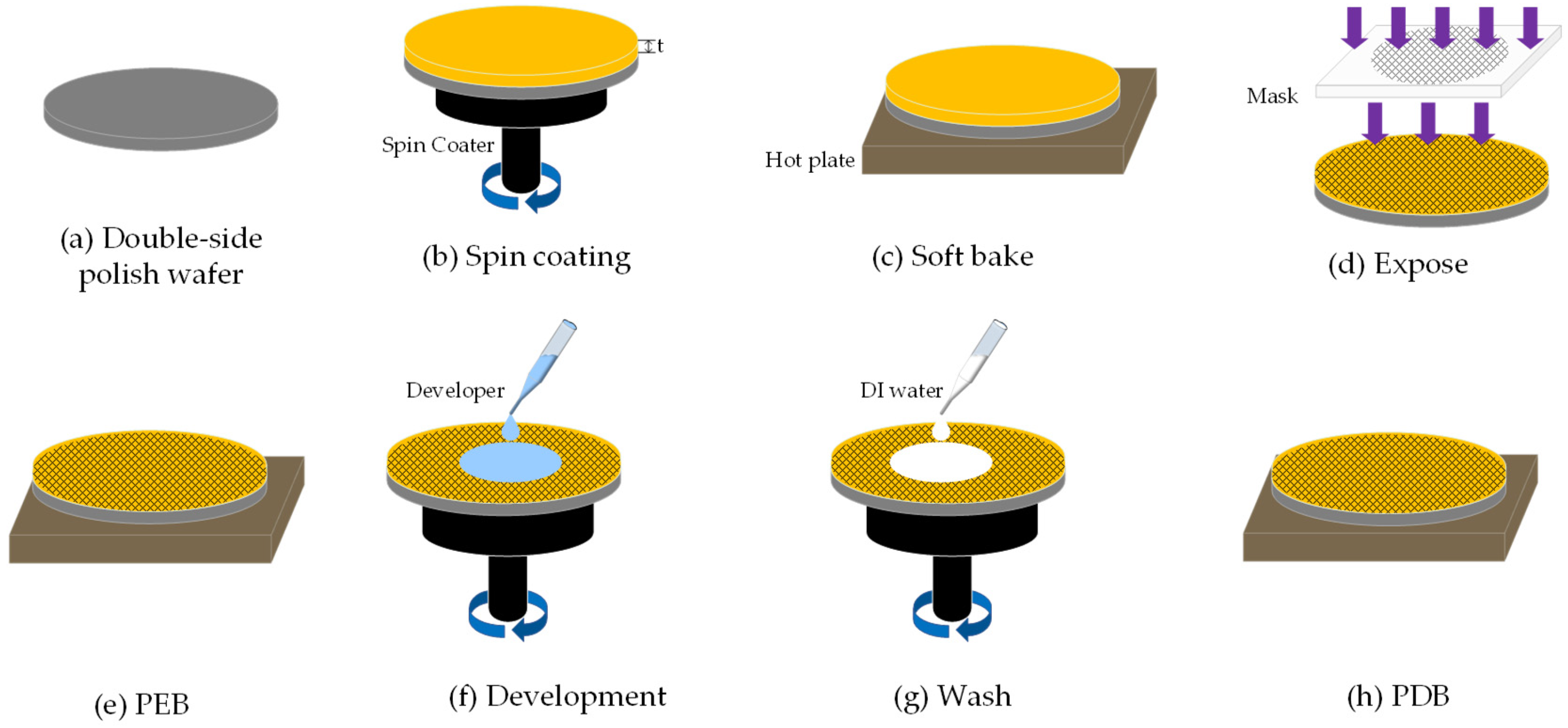
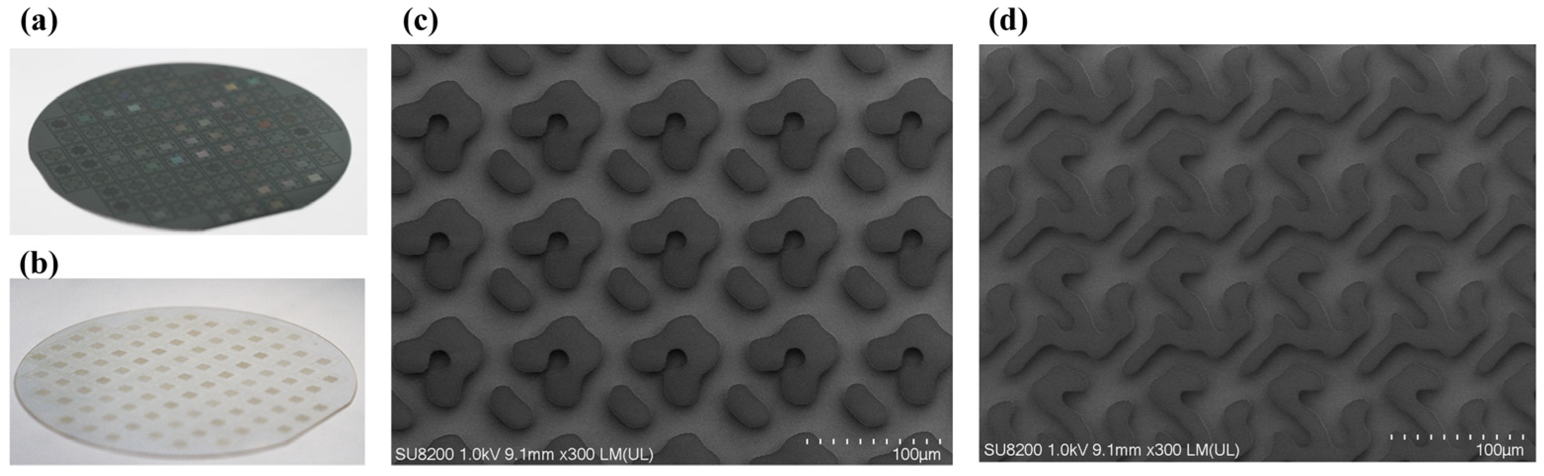
2.4. Microfabrication Technique
2.5. Charzcterization of DOE
3. Results and Discussion
3.1. Design of the DOE Beam Splitter
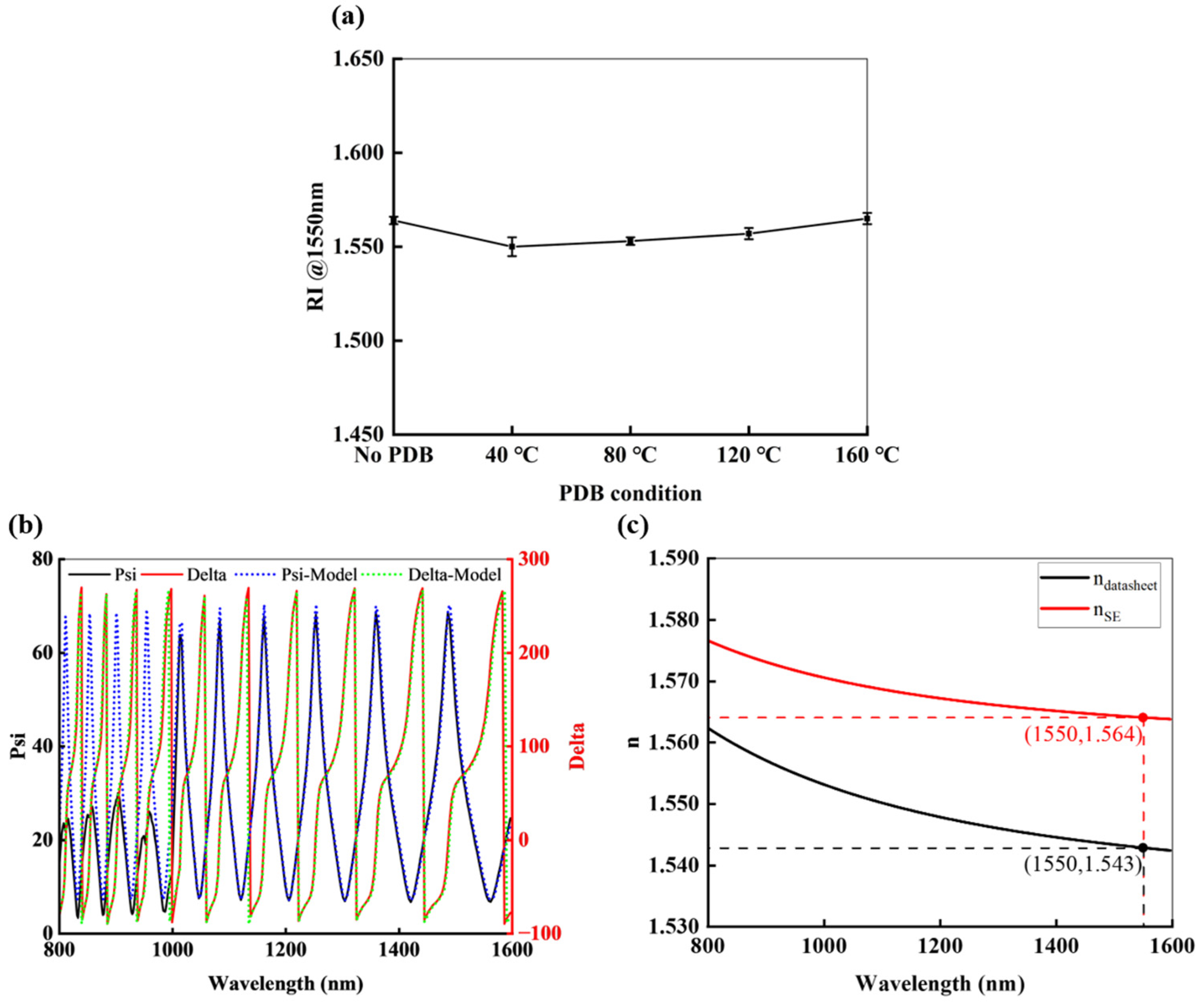
3.2. Refractive Index of the Morphology Layer
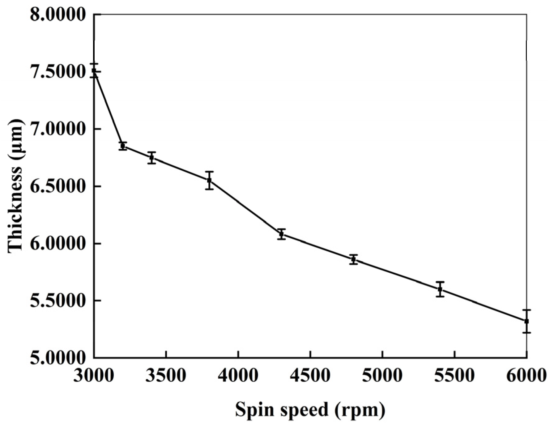
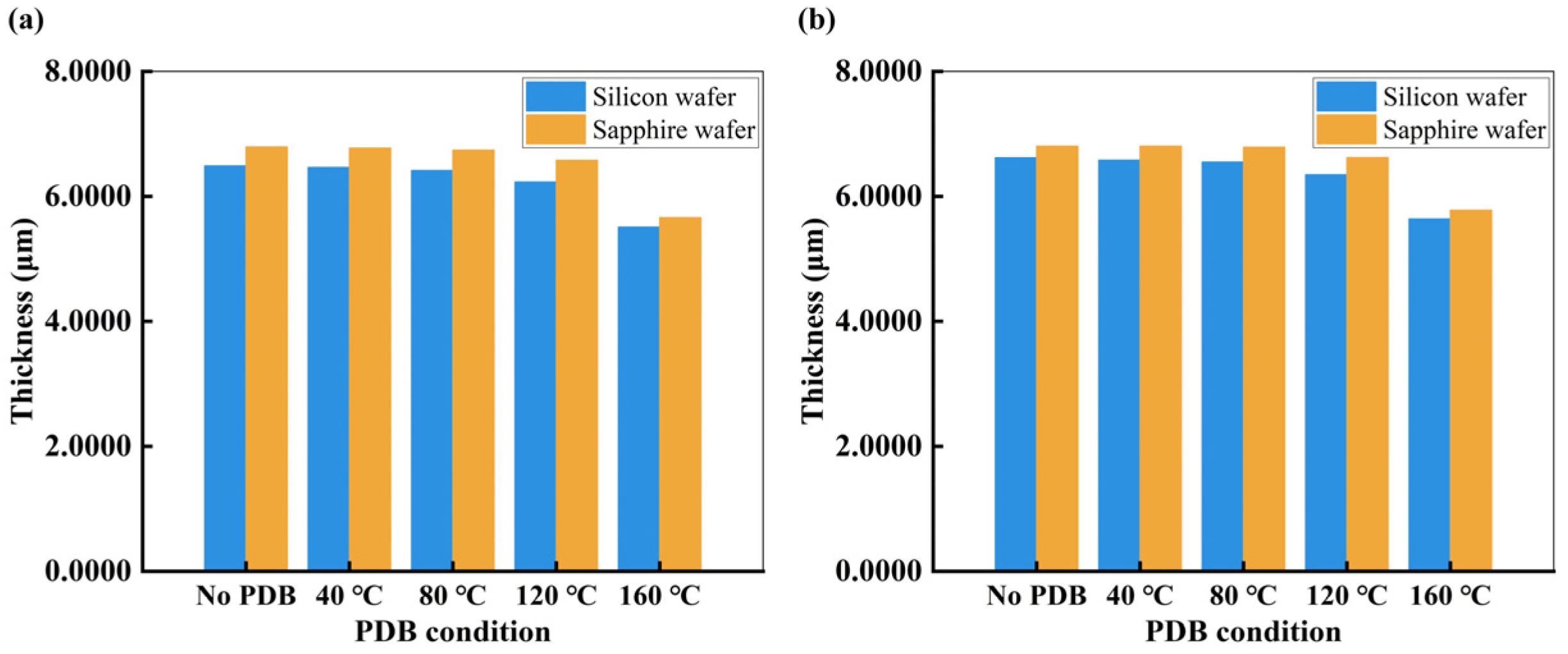
3.3. Thickness of the Morphology Layer
3.4. Wafer Transmittance (Silicon vs. Sapphire)
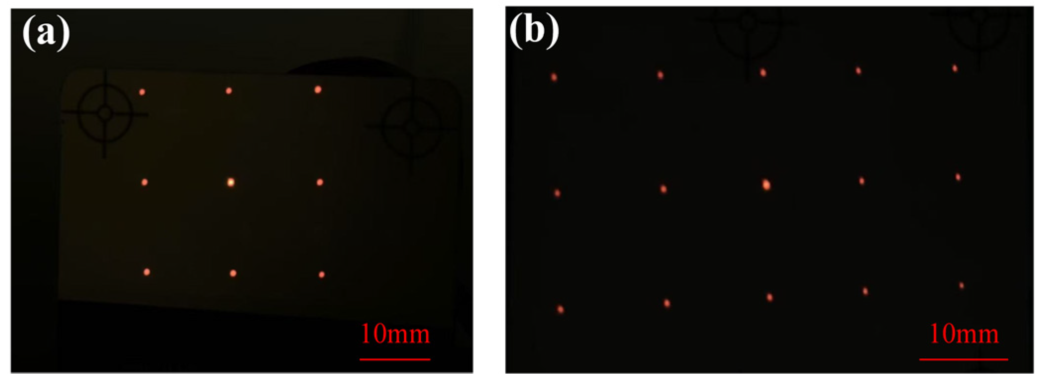
3.5. Comparison of Simulation and Experiement
4. Conclusions
Author Contributions
Funding
Data Availability Statement
Conflicts of Interest
References
- Liu, K.; Zhou, C.; Wei, S.; Wang, S.; Fan, X.; Ma, J. Optimized stereo matching in binocular three-dimensional measurement system using structured light. Appl. Opt. 2014, 53, 6083–6090. [Google Scholar] [CrossRef] [PubMed]
- Wang, H.; Wang, H.; Zhang, W.; Yang, J.K.W. Toward Near-Perfect Diffractive Optical Elements via Nanoscale 3D Printing. ACS Nano 2020, 14, 10452–10461. [Google Scholar] [CrossRef] [PubMed]
- Liu, X.; Chen, W.; Ma, Y.; Xie, Y.; Zhou, J.; Zhu, L.; Xu, Y.; Zhu, J. Enhancing THz fingerprint detection on the planar surface of an inverted dielectric metagrating. Photon. Res. 2022, 10, 2836–2845. [Google Scholar] [CrossRef]
- Werdehausen, D. Fundamentals of Effective Materials and Diffractive Optics. In Nanocomposites as Next-Generation Optical Materials: Fundamentals, Design and Advanced Applications; Werdehausen, D., Ed.; Springer International Publishing: Cham, Switzerland, 2021; pp. 15–31. [Google Scholar]
- Hemayat, S.; Hsu, L.; Ha, J.; Ndao, A. Near-unity uniformity and efficiency broadband meta-beam-splitter/combiner. Opt. Express 2023, 31, 3984–3997. [Google Scholar] [CrossRef]
- Ni, Y.; Chen, S.; Wang, Y.; Tan, Q.; Xiao, S.; Yang, Y. Metasurface for Structured Light Projection over 120° Field of View. Nano Lett. 2020, 20, 6719–6724. [Google Scholar] [CrossRef]
- Zhu, J.; Ning, Y.; Xie, L.; Dong, S.; Cheng, X.; Wang, Z.; Chen, Y. Dispersion-engineered broadband diffractive optical elements with multilayer subwavelength structures. Appl. Opt. 2023, 62, B19–B24. [Google Scholar] [CrossRef]
- He, L.; Chen, X.; Yang, Y.; Liu, X.; Chen, Y.; Xu, L.; Gu, C. Using high-diffraction-efficiency holographic optical elements in a full-color augmented reality display system. Opt. Express 2023, 31, 29843–29858. [Google Scholar] [CrossRef]
- Wu, Y.; Pan, C.; Gao, Y.; Lu, C.; Zhang, Y.; Huang, Z. Design of ultra-compact augmented reality display based on grating waveguide with curved variable-period grating. Opt. Commun. 2023, 529, 128980. [Google Scholar] [CrossRef]
- Vandenhouten, R.; Hermerschmidt, A.; Fiebelkorn, R. Design and quality metrics of point patterns for coded structured light illumination with diffractive optical elements in optical 3D sensors. In Proceedings of the SPIE Digital Optical Technologies, Munich, Germany, 25–29 June 2017; Volume 10335. [Google Scholar]
- Hermerschmidt, A.; Bedau, D.; Eichler, H.J. Multiple beam coupling and simultaneous build-up of different light-induced gratings in BaTiO3. In Proceedings of the Photorefractive Effects, Materials, and Devices, La Colle sur Loup, France, 17 June 2003; p. 326. [Google Scholar]
- Kalima, V.; Pietarinen, J.; Siitonen, S.; Immonen, J.; Suvanto, M.; Kuittinen, M.; Mönkkönen, K.; Pakkanen, T.T. Transparent thermoplastics: Replication of diffractive optical elements using micro-injection molding. Opt. Mater. 2007, 30, 285–291. [Google Scholar] [CrossRef]
- Hans, L.; Prater, K.; Kilchoer, C.; Scharf, T.; Herzig, H.P.; Hermerschmidt, A. Wafer-level microstructuring of glassy carbon. In Proceedings of the SPIE MOEMS-MEMS, San Francisco, CA, USA, 1–6 February 2014; Volume 8974. [Google Scholar]
- Prater, K.; Dukwen, J.; Scharf, T.; Herzig, H.P.; Plöger, S.; Hermerschmidt, A. Micro-structuring of glassy carbon for precision glass molding of binary diffractive optical elements. Opt. Mater. Express 2016, 6, 3407–3416. [Google Scholar] [CrossRef]
- Xiong, Z.; Kunwar, P.; Soman, P. Hydrogel-Based Diffractive Optical Elements (hDOEs) Using Rapid Digital Photopatterning. Adv. Opt. Mater. 2021, 9, 2001217. [Google Scholar] [CrossRef] [PubMed]
- Ripoll, O.; Kettunen, V.; Herzig, H.P. Review of iterative Fourier-transform algorithms for beam shaping applications. Opt. Eng. 2004, 43, 2549–2556. [Google Scholar] [CrossRef]
- Li, J.; Zhang, F.; Pu, M.; Guo, Y.; Li, X.; Ma, X.; Wang, C.; Luo, X. Quasi-Continuous Metasurface Beam Splitters Enabled by Vector Iterative Fourier Transform Algorithm. Materials 2021, 14, 1022. [Google Scholar] [CrossRef] [PubMed]
- Yan, Y.; Fan, Z.; Sun, G.; Tian, K. Diffractive optical element design based on vector diffraction theory and improved PSO-SA algorithm. Opt. Eng. 2023, 62, 025103. [Google Scholar] [CrossRef]
- Zhou, X.; Song, Q.; Yang, X.; Cai, W. Generating phase-only diffractive optical elements using adaptive constraints in the Fourier domain. Opt. Commun. 2023, 535, 129360. [Google Scholar] [CrossRef]
- Zhang, Q.; Lin, P.; Wang, C.; Zhang, Y.; Yu, Z.; Liu, X.; Lu, Y.; Xu, T.; Zheng, Z. Neural-Optic Co-Designed Polarization-Multiplexed Metalens for Compact Computational Spectral Imaging. Laser Photonics Rev. 2024, 18, 2400187. [Google Scholar] [CrossRef]
- Ma, G.; Yu, J.; Zhu, R.; Zhou, C. Optical multi-imaging–casting accelerator for fully parallel universal convolution computing. Photon. Res. 2023, 11, 299–312. [Google Scholar] [CrossRef]
- Xu, C.; Pang, H.; Cao, A.; Deng, Q. Alternative Design of Binary Phase Diffractive Optical Element with Non-π Phase Difference. Appl. Sci. 2021, 11, 1116. [Google Scholar] [CrossRef]
- Silalahi, H.M.; Chiang, Y.-C.; Lin, S.-H.; Jiang, Y.-R.; Huang, C.-Y. Manipulation of Photonic Jets of Topological Gratings Comprising ITO Strips and Nanowalls Using Refractive Indices of Dielectric Nanofilms. Laser Photonics Rev. 2024, 18, 2300659. [Google Scholar] [CrossRef]
- Jin, M.; Hu, Z.; Liu, X.; Li, G. Nonlinear Optical Wavefront Engineering with Geometric Phase Controlled All-Dielectric Metadevice. Laser Photonics Rev. 2023, 17, 2300174. [Google Scholar] [CrossRef]
- Wu, C.-H.; Chen, W.-S. Injection molding and injection compression molding of three-beam grating of DVD pickup lens. Sens. Actuators A Phys. 2006, 125, 367–375. [Google Scholar] [CrossRef]
- Schauer, S.; Meier, T.; Reinhard, M.; Röhrig, M.; Schneider, M.; Heilig, M.; Kolew, A.; Worgull, M.; Hölscher, H. Tunable Diffractive Optical Elements Based on Shape-Memory Polymers Fabricated via Hot Embossing. ACS Appl. Mater. Interfaces 2016, 8, 9423–9430. [Google Scholar] [CrossRef] [PubMed]
- Karin, P.; Julia, D.; Toralf, S.; Hans Peter, H.; Sven, P.; Andreas, H. Precision glass molding of high-resolution diffractive optical elements. In Proceedings of the SPIE Photonics Europe, Brussels, Belgium, 3–7 April 2016; p. 98880U. [Google Scholar]
- Orange-Kedem, R.; Nehme, E.; Weiss, L.E.; Ferdman, B.; Alalouf, O.; Opatovski, N.; Shechtman, Y. 3D printable diffractive optical elements by liquid immersion. Nat. Commun. 2021, 12, 3067. [Google Scholar] [CrossRef] [PubMed]
- Kim, D.C.; Hermerschmidt, A.; Dyachenko, P.; Scharf, T. Inverse design and demonstration of high-performance wide-angle diffractive optical elements. Opt. Express 2020, 28, 22321–22333. [Google Scholar] [CrossRef]
- Hao, H.; Tingting, Z.; Qiang, S.; Xiaodong, Y. Wide angle 2D beam splitter design based on vector diffraction theory. Opt. Commun. 2019, 434, 28–35. [Google Scholar] [CrossRef]
- Dai, X.; Zhang, H.; Hu, Y.; Jing, G.; Zhang, Z.; Fan, G. An improved Fourier modal method for design of metasurface diffractive optical elements. J. Opt. 2024, 26, 065103. [Google Scholar] [CrossRef]
- Orange kedem, R.; Opatovski, N.; Xiao, D.; Ferdman, B.; Alalouf, O.; Kumar Pal, S.; Wang, Z.; von der Emde, H.; Weber, M.; Sahl, S.J.; et al. Near index matching enables solid diffractive optical element fabrication via additive manufacturing. Light Sci. Appl. 2023, 12, 222. [Google Scholar] [CrossRef]
- Hilfiker, J.N.; Hong, N.; Schoeche, S. Mueller matrix spectroscopic ellipsometry. Adv. Opt. Technol. 2022, 11, 59–91. [Google Scholar] [CrossRef]


| DOE Types | Simulation and Experiment of DOE | Thickness (μm) | η (%) | σ (%) |
|---|---|---|---|---|
| 3 × 3 | Simulation | 6.8706 (ideal) | 34.91 | 12.58 |
| Experiment | 6.8272 (determined) | 30.64 | 18.84 | |
| 6.8044 | 30.89 | 24.72 | ||
| 6.9805 | 31.71 | 29.88 | ||
| 3 × 5 | Simulation | 6.8706 (ideal) | 39.72 | 4.34 |
| Experiment | 6.8611 (determined) | 35.29 | 9.83 | |
| 6.7570 | 36.97 | 18.94 | ||
| 6.9842 | 35.74 | 20.63 |
| DOE Types | Simulation and Experiment of DOE | Thickness (μm) | η (%) | σ (%) |
|---|---|---|---|---|
| 3 × 3 | Simulation | 6.8706 (ideal) | 56.55 | 12.58 |
| Experiment | 6.8947 (determined) | 52.61 | 15.42 | |
| 6.8401 | 52.69 | 16.73 | ||
| 6.9001 | 52.76 | 20.61 | ||
| 3 × 5 | Simulation | 6.8706 (ideal) | 64.31 | 4.34 |
| Experiment | 6.8828 (determined) | 60.69 | 8.61 | |
| 6.9002 | 60.41 | 17.66 | ||
| 6.7994 | 61.88 | 26.44 |
Disclaimer/Publisher’s Note: The statements, opinions and data contained in all publications are solely those of the individual author(s) and contributor(s) and not of MDPI and/or the editor(s). MDPI and/or the editor(s) disclaim responsibility for any injury to people or property resulting from any ideas, methods, instructions or products referred to in the content. |
© 2025 by the authors. Licensee MDPI, Basel, Switzerland. This article is an open access article distributed under the terms and conditions of the Creative Commons Attribution (CC BY) license (https://creativecommons.org/licenses/by/4.0/).
Share and Cite
Dai, X.; Hu, Y.; Niu, B.; Dai, Q.; Ao, Y.; Zhang, H.; Jing, G.; Li, Y.; Fan, G. A Microfabrication Technique for High-Performance Diffractive Optical Elements Tailored for Numerical Simulation. Nanomaterials 2025, 15, 138. https://doi.org/10.3390/nano15020138
Dai X, Hu Y, Niu B, Dai Q, Ao Y, Zhang H, Jing G, Li Y, Fan G. A Microfabrication Technique for High-Performance Diffractive Optical Elements Tailored for Numerical Simulation. Nanomaterials. 2025; 15(2):138. https://doi.org/10.3390/nano15020138
Chicago/Turabian StyleDai, Xingang, Yanjun Hu, Bowen Niu, Qun Dai, Yu Ao, Hongru Zhang, Gaoshan Jing, Yuan Li, and Guofang Fan. 2025. "A Microfabrication Technique for High-Performance Diffractive Optical Elements Tailored for Numerical Simulation" Nanomaterials 15, no. 2: 138. https://doi.org/10.3390/nano15020138
APA StyleDai, X., Hu, Y., Niu, B., Dai, Q., Ao, Y., Zhang, H., Jing, G., Li, Y., & Fan, G. (2025). A Microfabrication Technique for High-Performance Diffractive Optical Elements Tailored for Numerical Simulation. Nanomaterials, 15(2), 138. https://doi.org/10.3390/nano15020138