Abstract
A two-step annealing treatment was applied on a fully transparent amorphous InGaZnO4 (a-IGZO) top-gate thin-film transistor (TG-TFT) to improve the device performance. The electrical properties and stabilities of a-IGZO TG TFTs were significantly improved as the first-annealing temperature increased from 150 °C to 350 °C with a 300 °C second-annealing treatment. The a-IGZO TG-TFT with the 300 °C first-annealing treatment demonstrated the overall best performance, which has a mobility of 13.05 cm2/(V·s), a threshold voltage (Vth) of 0.33 V, a subthreshold swing of 130 mV/dec, and a Ion/Ioff of 1.73 × 10⁸. The Vth deviation (ΔVth) was −0.032 V and −0.044 V, respectively, after a 7200 s positive and negative bias stress under the gate bias voltage VG = ±3 V and VD = 0.1 V. The Photoluminescence spectra results revealed that the distribution and the density of defects in a-IGZO films were changed after the first-annealing treatment, whereas the X-ray photoelectron spectroscopy results displayed that contents of the oxygen vacancy and Ga-O bond varied in annealed a-IGZO films. In addition, a-IGZO TG-TFTs had achieved a transmittance of over 90%. Research on the effects of the first-annealing treatment will contribute to the fabrication of highly stable top-gate TFTs in the fields of transparent flexible electronics.
1. Introduction
The top-gate (TG)-structured amorphous InGaZnO4 (a-IGZO) thin-film transistor (TFT) was widely used in fields of fingerprint sensors, transparent displays, and flexible electronics [1,2,3,4,5,6] due to its high gate control capability and excellent stability. The high stability of a-IGZO TG-TFTs requires a certain special treatment on the a-IGZO active layer, such as annealing in different gas atmospheres, plasma gas treatment, or covering a passivation layer [5,7,8,9,10,11,12]. The aforementioned various treatments could improve the bonding state of metal ions and oxygen atoms both on the surface and interface, and inside the a-IGZO active layer [9,13].
For TG-TFTs, the gate dielectric layer is deposited after the semiconductor active layer. The bonding state in the a-IGZO active layer would degrade during the deposition of Al2O3 gate dielectric material in the fabrication of TG-TFTs [5,14,15,16]. Especially, the quantity of oxygen vacancy (VO) and the distribution of O defects in a-IGZO were significantly altered when the Al2O3 top-gate dielectric is grown through the atomic layer deposition (ALD) process, leading to the degeneration in the electrical performance of a-IGZO TG-TFTs [8,9,10,14,17]. The variation in oxygen-related states mainly originated from oxygen outgassing from a-IGZO during the deposition of Al2O3 in the ALD high-temperature vacuum environment [18]. Thermal annealing treatments in air or O2 after gate dielectric deposition have been considered to be an effective method to improve oxygen-related states at the a-IGZO-Al2O3 interface and within the a-IGZO and Al2O3 layers, and increase the film density and uniformity [5,14,15,16], which mainly relies on oxygen diffusion mechanisms [5,14,15,19]. However, the diffusion of external oxygen into the a-IGZO active layer is significantly hindered due to the passivation effect of the Al2O3 top-gate dielectric, resulting in only partly eliminating the degradation of a-IGZO. In addition, oxygen vacancies are passivated by the hydrogen diffusing from the precursor residue of trimethylaluminum (TMA) in Al2O3 and the deficiency of oxygen in a-IGZO lead to the negative degradation of the threshold voltage (Vth) of a-IGZO TG-TFTs [16,19]. Therefore, another annealing treatment on a-IGZO in air or O2 before the gate dielectric deposition was proposed in some reports to resist the degradation of a-IGZO due to the formation of metal–oxygen (M-O) bonds, reducing the VO and O defects and densifying a-IGZO films [20,21]. In previous reports, the effect on the performance of devices and the mechanism of the annealing treatment after gate dielectric deposition have been thoroughly investigated [5,11,16,22], while the effect and underlying mechanism of the annealing treatment of a-IGZO before the gate dielectric deposition are seldom reported.
In this work, a two-step annealing treatment was applied during the fabrication of the TG-TFT. The annealing treatment on the a-IGZO active layer before ALD-Al2O3 gate dielectric deposition is defined as the first annealing (first-annealing), while the annealing of a-IGZO TG-TFTs after Al2O3 coverage is defined as the second annealing (second-annealing). The mechanism on a-IGZO and a-IGZO TFTs of the second-annealing treatment had been reported in our previous study [16]. Herein, the effect and mechanism of the first-annealing treatment on the a-IGZO active layer and the stability of a-IGZO TG-TFTs were systematically investigated based on a fully transparent a-IGZO TG-TFT fabricated under different first-annealing conditions. The UV–Vis optical transmission spectrum was used to obtain the transmittance of the a-IGZO TG-TFT. The photoluminescence (PL) spectroscopy and X-ray photoelectron spectroscopy (XPS) were employed to analyze the first-annealing mechanism through investigating the distribution and the content of defects within the a-IGZO layer.
2. Materials and Methods
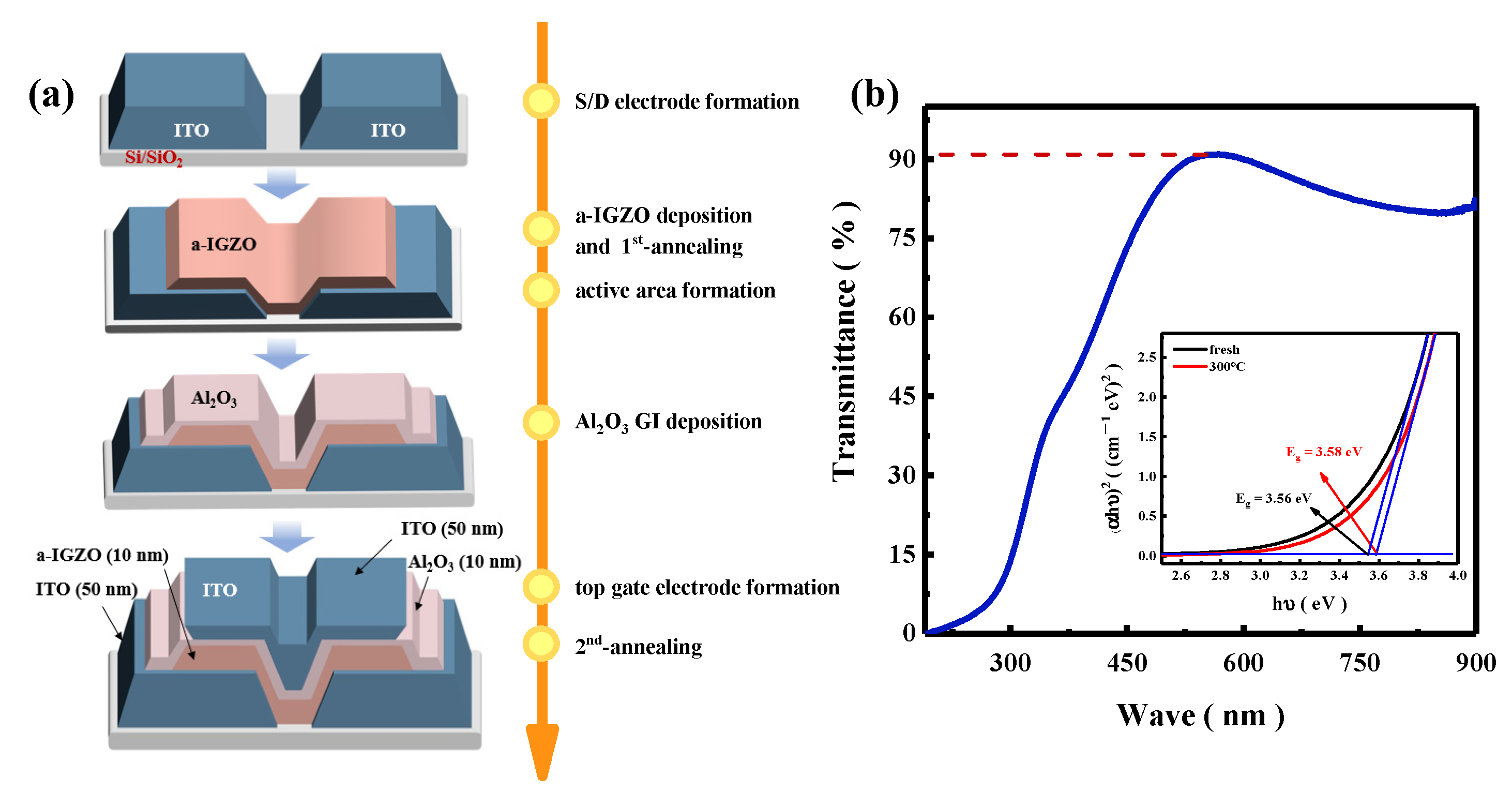
Figure 1a shows a schematic of the fabricating process sequence and major processing steps, respectively, of the top-gate bottom-contact a-IGZO TFT in this work. The fully transparent staggered TG-TFTs were fabricated on a cleaned SiO2 (100 nm)/Si substrate. Firstly, ITO source and drain (S/D) electrodes were deposited by radio-frequency (RF) magnetron sputtering (Denton Vacuum, Moorestown, NJ, USA) at 60 W in an Ar atmosphere under a pressure of 0.43 mtorr for 840 s. The S/D regions were defined by photolithography, and outside regions were etched by CH4 and H2 at 60 °C using inductively coupled plasma reactive-ion etching (ICP-RIE) (Oxford Instruments, London, UK). Secondly, the a-IGZO channel was deposited through RF magnetron sputtering at 90 W in a pure Ar atmosphere from a ceramic target with a molar ratio of In2O3:Ga2O3:ZnO = 1:1:1 at room temperature (RT). Right after the deposition of a-IGZO layer, the first-annealing treatment was carried out in air (the air humidity is 40%) for 1 h, which the first-annealing treatment temperatures were controlled between 150 °C and 350 °C with a step of 50 °C. The a-IGZO channel regions were defined as 10 μm × 10 μm by photolithography, and were etched by CH4 and H2 at 20 °C using ICP-RIE technology. Subsequently, the Al2O3 gate insulator (GI) was deposited through thermal-ALD (Kemicro, Jiaxing, China) at 150 °C with trimethylaluminum (TMA) and H2O as the aluminum and oxygen precursors, respectively, and N2 as the purge gas. The pulse times for TMA, H2O, and N2 were 0.03 s, 0.02 s, and 30 s, respectively. Finally, ITO gate electrodes were deposited by RF magnetron sputtering in an Ar atmosphere and defined by lift-off processes. The second-annealing treatment was carried out at 300 °C in air for 1 h after the fabrication of a-IGZO TFTs finished. Additionally, the layer thicknesses of the ITO S/D electrodes, a-IGZO channel, Al2O3 GI, and ITO gate electrode were measured using atomic force microscope (AFM) (Being Nano-Instruments, Guangzhou, China) and found to be 50 nm, 24 nm, 10 nm, and 50 nm, respectively.
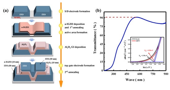
Figure 1.
(a) Schematic of fabrication process, and (b) the measured transmittance of the a-IGZO TG-TFT device across various wavelengths, and the insert is the calculated band gap energy for a 130 nm a-IGZO film on a quartz substrate.
All electrical measurements of the a-IGZO TG-TFTs were performed using an Agilent B1500A parameter analyzer connected to Cascade (CASCADE MICROTECH, Hsinchu City, Taiwan) EPS1500TRIAX (Keysight, Santa Rosa, CA, USA) probe station at RT in a dark ambient atmosphere. The PL spectrum was obtained using a Renishaw inVia Raman (Renishaw, London, UK) spectrometer equipped with a 325 nm wavelength laser. XPS spectra were obtained on a Thermo Scientific K-Alpha XPS (Thermo Scientific, Waltham, MA, USA) system with monochromatic Al Kα X-ray (1486.7 eV) radiation and were calibrated by the C 1s peak (~284.8 eV).
3. Results
3.1. Optical and Electric Characteristics of TG-TFTs
The transmittance of the fully transparent staggered a-IGZO TG-TFT was shown in Figure 1b. The transmittance of the a-IGZO TG-TFT obtained by the UV–Vis optical transmission spectra had achieved over 90% (with quartz as the substrate) in the visible light range. The bandgap width of the a-IGZO film was also calculated, as shown in the insert of Figure 1b. The bandgap of the fresh a-IGZO film (without annealing) was 3.56 eV, while the bandgap of the a-IGZO film with annealing at 300 °C for 1h was 3.58 eV. This might be due to the significant reduction in tail states in the a-IGZO film during annealing, which results in a blue-shifted optical bandgap [23]. The pleasant transmittance of the TG-TFT was mainly attributed to the wide bandgap of the a-IGZO material, which is benefit for applications in transparent flexible electronics and smart wearable devices.
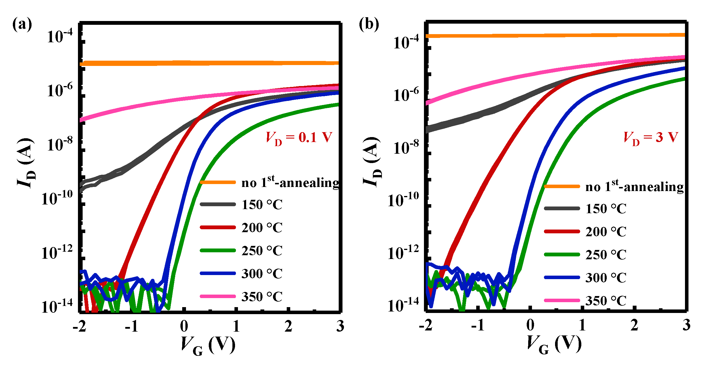
Figure 2a,b displayed the transfer characteristics of TG-TFTs with different first-annealing treatments. As shown in Figure 2a,b, the TG-TFT without the first-annealing treatment did not show the switching characteristic, which indicated that the degradation of the a-IGZO layer without first-annealing was most severe after the deposition of Al2O3. During the deposition process of Al2O3, the a-IGZO film was exposed to a high-temperature vacuum environment for a long time, which led to the following oxygen evolution reaction in the a-IGZO film, M-O + M-O → M-M + O2↑, resulting in the loss of the O atom and the generation of oxygen vacancies in the a-IGZO film [18]. The first-annealing treatment could increase the oxygen content and M-O binding energy inside IGZO before the coverage of Al2O3, and then helping the a-IGZO film resist O deficiency caused by the Al2O3 deposition process. There was a significant change in the transfer characteristics of the transistor after the introduction of the first-annealing treatment. The TFTs with first-annealing at 150 °C and 350 °C did not exhibit obvious switching characteristics, which were attributed to the formation of extensive shallow donor states and the creation of new trap states in a-IGZO [9], respectively. The shallow donor states generated during the first-annealing treatment would release electrons into the conduction band of a-IGZO, and the increase in the carrier concentration led to the increase in the drain current, resulting in the improvement of the field-effect mobility. The TFTs with first-annealing treatment at 200 °C–300 °C exhibited good switching characteristics, with performance varying depending on the first-annealing temperature. The electrical parameters of the TG-TFTs, such as the threshold voltage (Vth), subthreshold swing (SS), field-effect mobility (μsat), and on/off current ratio (Ion/Ioff), were all extracted from the saturated transfer curve, as summarized in Table 1. The Vth-sat was shifting positively with increasing first-annealing temperature up to 250 °C, and then switching to a negative shift with further increasing first-annealing temperature. The turn-around Vth shift was associated with changes in the quantity and distribution of VO and O defects, and the bonding energy between metal ions and oxygen atom within the internal composition of a-IGZO films [9,17,24].
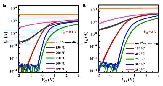
Figure 2.
(a,b) These are transfer characteristics of TG-TFTs with different first-annealing treatments under VD = 0.1 V and VD = 3 V, respectively.

Table 1.
Electrical characteristic parameters of TG-TFTs with different first-annealing temperature.
From Figure 2b and Table 1, the values of SS were 203 mV (200 °C), 137 mV (250 °C), and 130 mV (300 °C), and showing a declining trend as increasing the first-annealing temperature. It was reported that the SS was mainly influenced by the interfacial quality and defect states between the Al2O3 and the a-IGZO channel [25]. The excellent interfaces between a-IGZO and Al2O3 had been proven by the negligible hysteresis of the transfer curves as shown in Figure 2a,b. And the density of the trapping states (Nt) at the interface was extracted from the SS by the following formula:
where κB is Boltzmann’s constant, Cox is the unit area capacitance of 10 nm Al2O3, T was the temperature in Kelvin, and q is the electron charge. In this work, the Cox was 408 nF/cm2 obtained from the capacitance–voltage measurement. The calculated Nt value was within the range of 2.98 × 10¹²–6.10 × 10¹² eV−1cm−2 as shown in Table 1, and this result was also agreement with the previously reported value 3.0 × 10¹² eV−1cm−2 [25]. The improvement in SS performance with increasing the first-annealing temperature might be mainly attributed to the reduction of O defects and VO in the a-IGZO film [26].
3.2. Electrical Stability Test on a-IGZO TG-TFTs
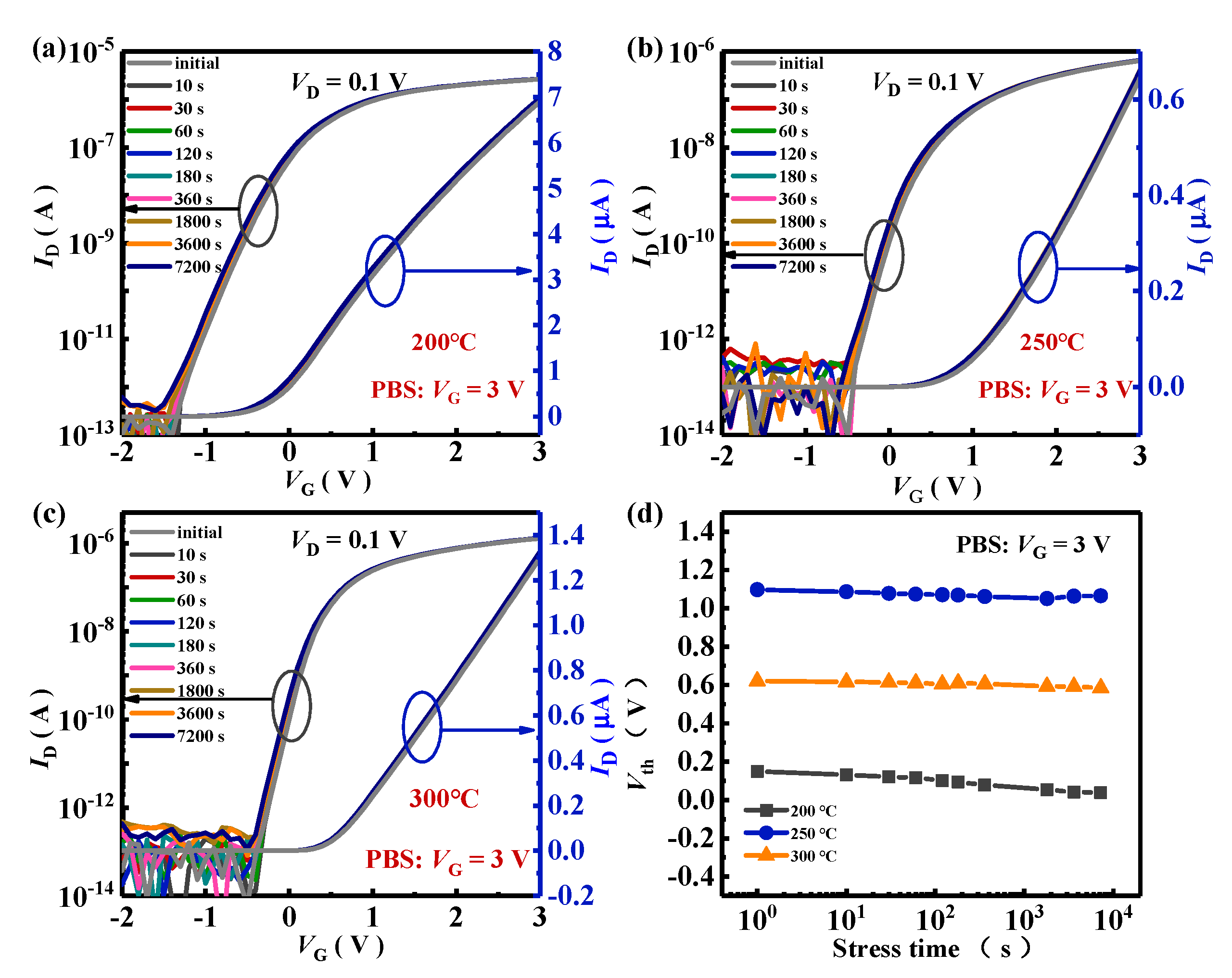
The electrical stability of a-IGZO TG-TFTs was further investigated. As depicted in Figure 3 and Figure 4, positive bias stress (PBS) and negative bias stress (NBS) measurements were performed on TG-TFTs under the test conditions of Vstress (gate bias voltage) = ±3 V at VD = 0.1 V. As displayed in Figure 3a–c, transfer curves of all TG-TFTs shifted very slightly in the negative direction after a positive stress duration of 7200 s, demonstrating an excellent resistance to PBS. And this extraordinary stability was mainly due to the good interface between the a-IGZO channel and the Al2O3 insulator [27,28,29]. Moreover, the negative shift in transfer curves was likely caused by the H-doping effect, which was resulting from the ALD-Al2O3 insulator due to the second-annealing treatment. This has been discussed in our previous published report [16]. The ALD-Al2O3 grown at low temperatures contains a large number of Al-OH bonds. Under the gate voltage electric field, hydrogen atoms of the Al-OH bond would detach and combine with O2− on the surface of a-IGZO to form OH−, releasing an electron into the conduction band of a-IGZO, resulting in a negative transfer shift [27]. The second-annealing treatment could reduce the content of Al-OH bonds in Al2O3 [16], thereby preventing the negative shift in the transfer curve. O-defects would be ionized by the gate bias electric field, and ionized O-defects would release electrons into the conduction band, resulting in a negative shift in the transfer curve. The deviations in Vth (ΔVth) between the initial and the 7200 s positive-biased transfer curves at VD = 0.1 V were −0.11 V (200 °C), −0.035 V (250 °C), and −0.032 V (300 °C), respectively. This result showed that the PBS stabilities of TG-TFTs had an obvious improvement with increasing first-annealing temperatures, with the TG-TFT first-annealed at 300 °C exhibiting the best PBS stability. The improvement in PBS stabilities might be due to the reduction in VO and the increase in bonds between the O atom and metal atom. Compared with In-O and Zn-O, the Ga-O bond energy is larger and more capable of resisting the damage of the gate bias electric field [30].
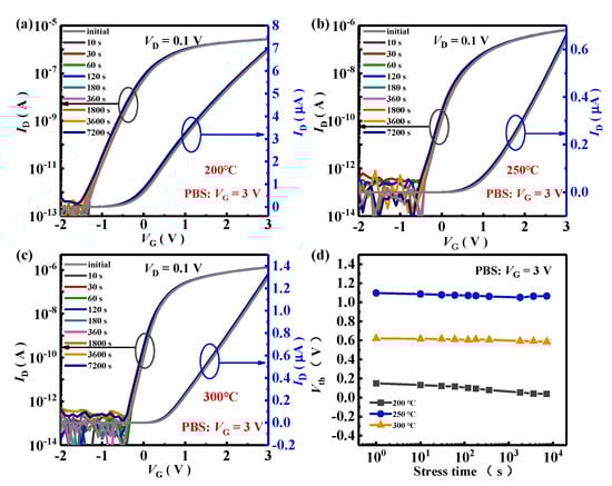
Figure 3.
PBS time evolution (under Vstress = 3 V and VD = 0.1 V at RT without illumination) of the transfer for a-IGZO TG-TFTs with first-annealing treatments at (a) 200 °C, (b) 250 °C, and (c) 300 °C, and (d) Vth shifts during the PBS process.

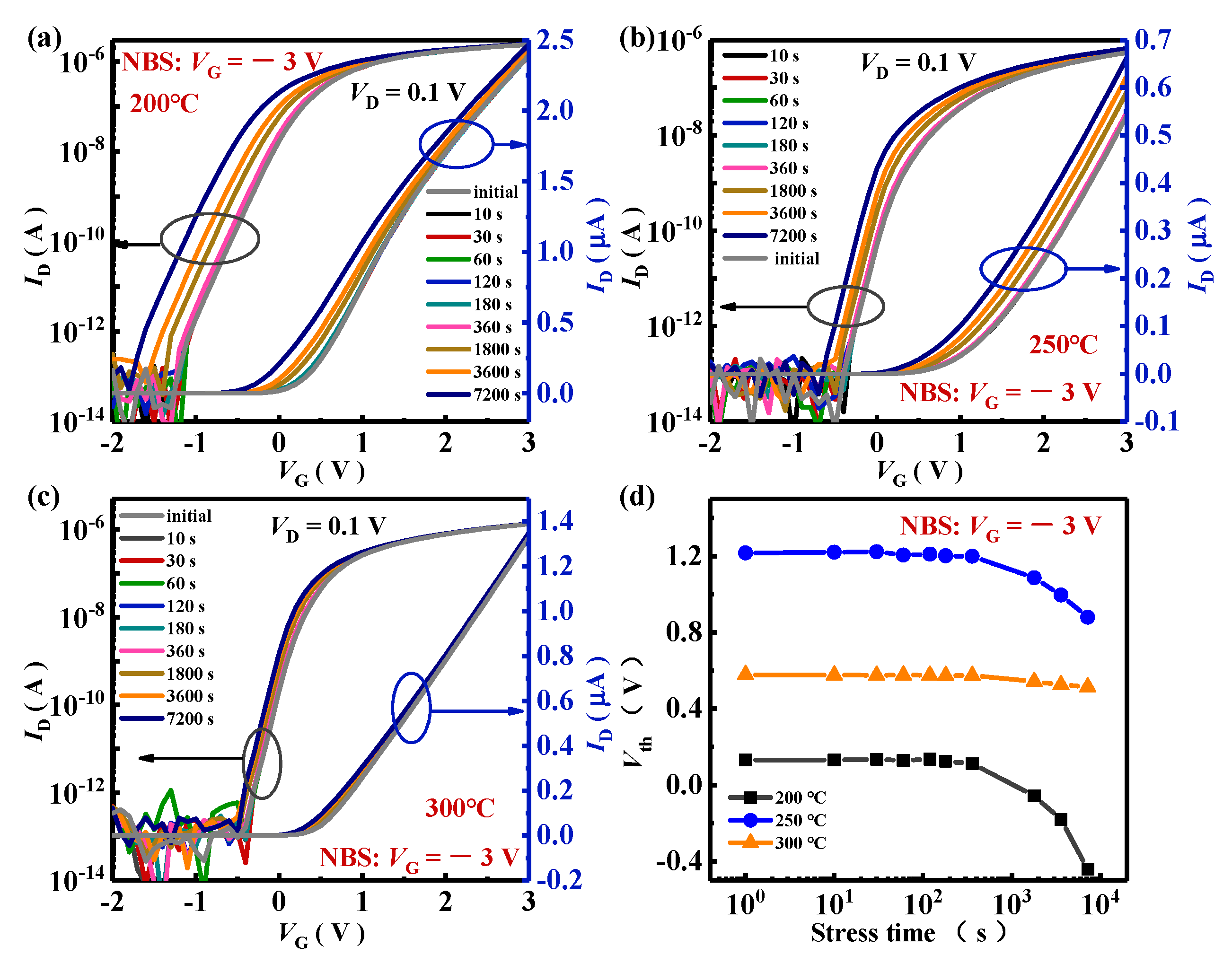
Figure 4.
NBS time evolution (under Vstress = −3 V and VD = 0.1 V at RT without illumination) of the transfer for a-IGZO TG-TFTs with first-annealing treatments at (a) 200 °C, (b) 250 °C, and (c) 300 °C, and (d) Vth shifts during the NBS process.
The NBS results of a-IGZO TG-TFTs were presented in Figure 4. The transfer characteristics of all TG-TFTs exhibited negative shifts after a 7200 s stress duration under the Vstress = −3 V condition, which is similar to the trends that appeared in other n-type oxide semiconductor (e.g., TiO2, SnO2) TFTs [31,32], as shown in Figure 4a–c. The negative shifts in Vth are attributed to the fact that holes were difficult to be generated in n-type oxide semiconductors [16]. The ΔVth values between the initial and the 7200 s negative-biased transfer curves at VD = 0.1 V were −0.573 V (200 °C), −0.335 V (250 °C), and −0.044 V (300 °C). It was evident that the NBS stabilities of the TG-TFTs were improved with increasing first-annealing temperature, with the 300 °C first-annealed device exhibiting the best NBS stability. The excellent NBS stability would make a-IGZO TG-TFTs very advantageous for applications in the field of transparent displays.
The best PBS and NBS stabilities were both obtained from TG-TFTs with the first-annealing treatment at 300 °C. In order to further understand the effect of the first-annealing treatment on the bias stress stability improvement of TG-TFTs, PL and XPS spectra were conducted on a-IGZO films with first-annealing treatments at 200 °C, 250 °C, and 300 °C.
3.3. First-Annealing Effect on a-IGZO Films
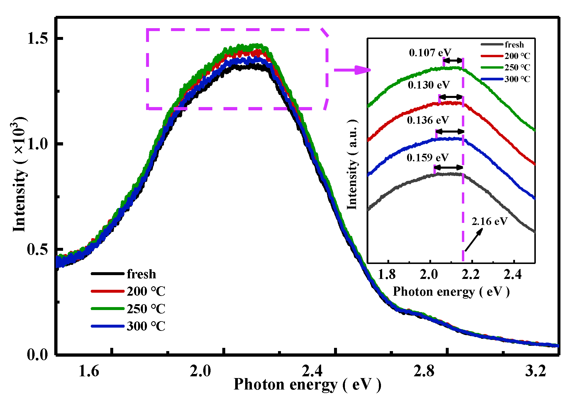
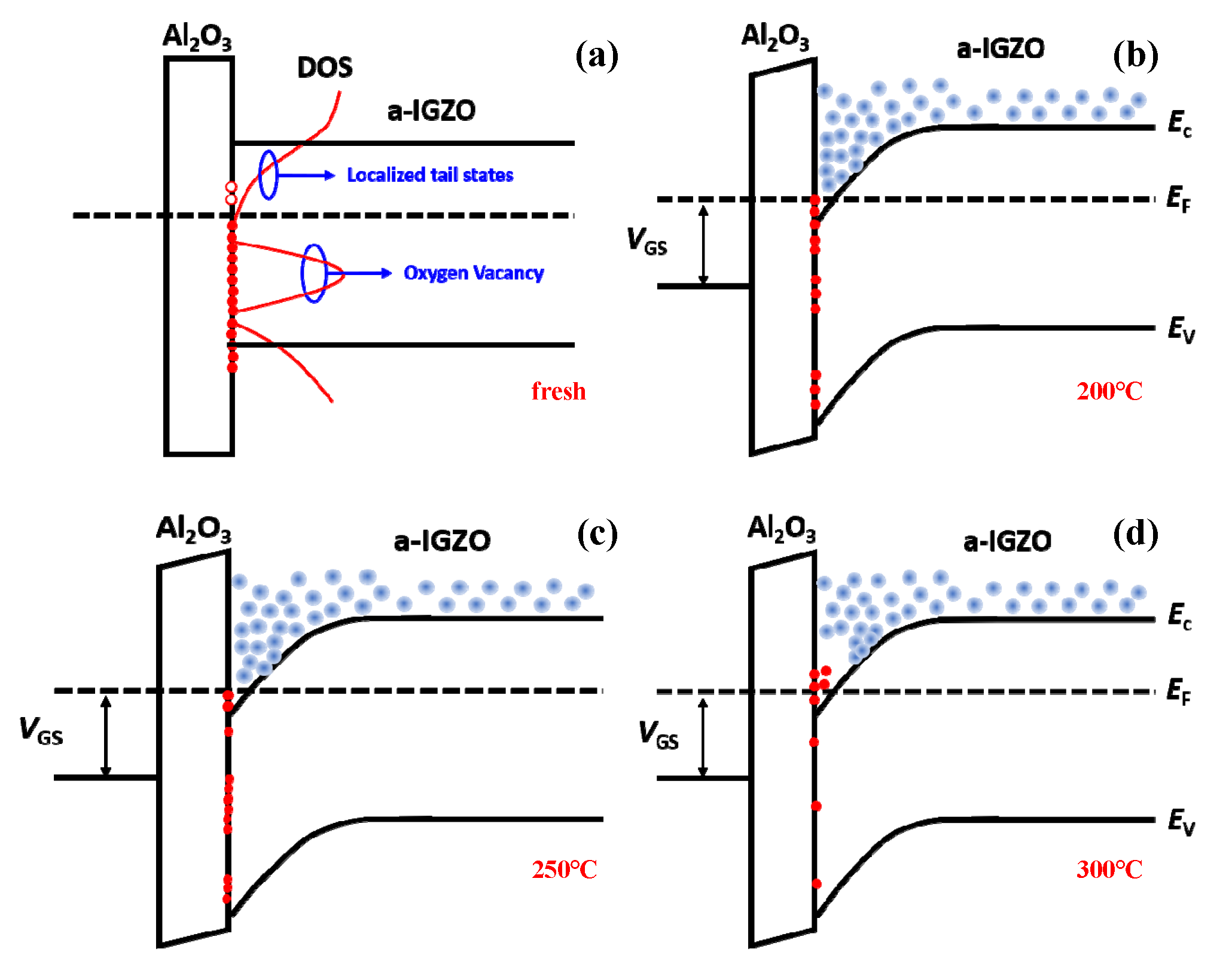
Figure 5 and the insert figure showed the PL spectra and separated PL spectra of a-IGZO films with first-annealing at fresh (no first-annealing), 200 °C, 250 °C, and 300 °C. Four broad emission peaks were found in the visible light range of 1.6~3.2 eV, which is consistent with previous reports [33,34,35,36]. From the insert of Figure 5, every peak was observed with a flat top, of which the maximum energy for all peaks was at 2.16 eV. The result meant that the deepest defect in all a-IGZO films was located at 2.16 eV below the conduction band bottom (VBM) [37]. In addition, the energy bands occupied by the flat top of the measured peaks were 0.159 eV (fresh), 0.130 eV (200 °C), 0.107 eV (250 °C), and 0.136 eV (300 °C), respectively. The peak intensity and width of the energy band of the flat top in the PL spectra may illustrate the density and the distribution range of defects in the a-IGZO film [34,35,38]. The flat band width of the a-IGZO film annealed at 300 °C in the PL spectrum decreased by 0.023 eV compared to the fresh a-IGZO film. The bandgap of a-IGZO increased by 0.02 eV after the 300 °C annealing treatment, as shown in the insert of Figure 1b. These results indicated that tail states at the bottom of the conduction band of the a-IGZO film shifted upward by about 0.02 eV after the 300 °C annealing treatment. The PL curve of the a-IGZO film with first-annealing at 250 °C exhibited the highest peak intensity and the narrowest energy band (0.107 eV) of the flat top, while the PL spectra of the a-IGZO film without first-annealing showed the lowest peak intensity and the widest energy band (0.159 eV). These results demonstrated that the O defects in the a-IGZO film with first-annealing at 250 °C were at the deepest energy level, which might result in the largest positive Vth observed in the corresponding TG-TFT, as shown in Figure 2a,b. The PL spectra of the a-IGZO film with the 300 °C first-annealing treatment showed a lower peak intensity but a wider energy band (0.136 eV) of the flat top compared to the 250 °C first-annealed a-IGZO film. This result might suggest that some shallow defect states were generated in the 300 °C first-annealed a-IGZO film as the overall number of defects decreased [9]. It is known that H2O is difficult to be adsorbed on the surface of a-IGZO when the temperature is above 300 °C. In addition, M-OH in a-IGZO reacted with another M-OH to evaporate a H2O molecule, and left an ionized oxygen vacancy and two electrons. This is why shallow defect states were generated in the 300 °C first-annealed a-IGZO film [17]. The band diagram explained the changes in the defects observed in the PL spectrum, as shown in Figure 6. In the a-IGZO film first-annealed at 200 °C, the VO concentration was significantly reduced compared to the fresh a-IGZO film, as shown in Figure 6b. The a-IGZO film first-annealed at 250 °C has a higher VO concentration than those first-annealed at 200 °C and 300 °C, with the VO states in a-IGZO first-annealed at 250 °C occupying the central region of the bandgap, as shown in Figure 6c. In contrast, the a-IGZO film first-annealed at 300 °C had a lower VO concentration compared to that first-annealed at 200 °C, but the VO were mainly distributed at shallower energy levels below the conduction band, as illustrated in Figure 6d. And this might be the reason for the higher mobility observed in the TG-TFT with the 300 °C first-annealing treatment compared to the TG-TFT with 250 °C first-annealed a-IGZO, as shown in Table 1.
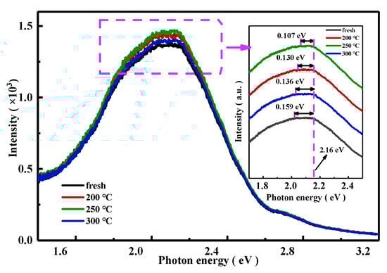
Figure 5.
PL spectra for a-IGZO films under different first-annealing temperatures of fresh, 200 °C, 250 °C, and 300 °C, respectively; insert is separated PL spectra in the range of 1.7–2.5 eV.
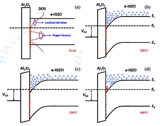
Figure 6.
Energy bands and carrier transport diagrams of TG-TFTs with different first-annealing temperatures of fresh, 200 °C, 250 °C, and 300 °C: (a) subthreshold region for the fresh TG-TFT, and on-state regions for (b) 200 °C first-annealed TG-TFT, (c) 250 °C first-annealed TG-TFT, and (d) 300 °C first-annealed TG-TFT, respectively.
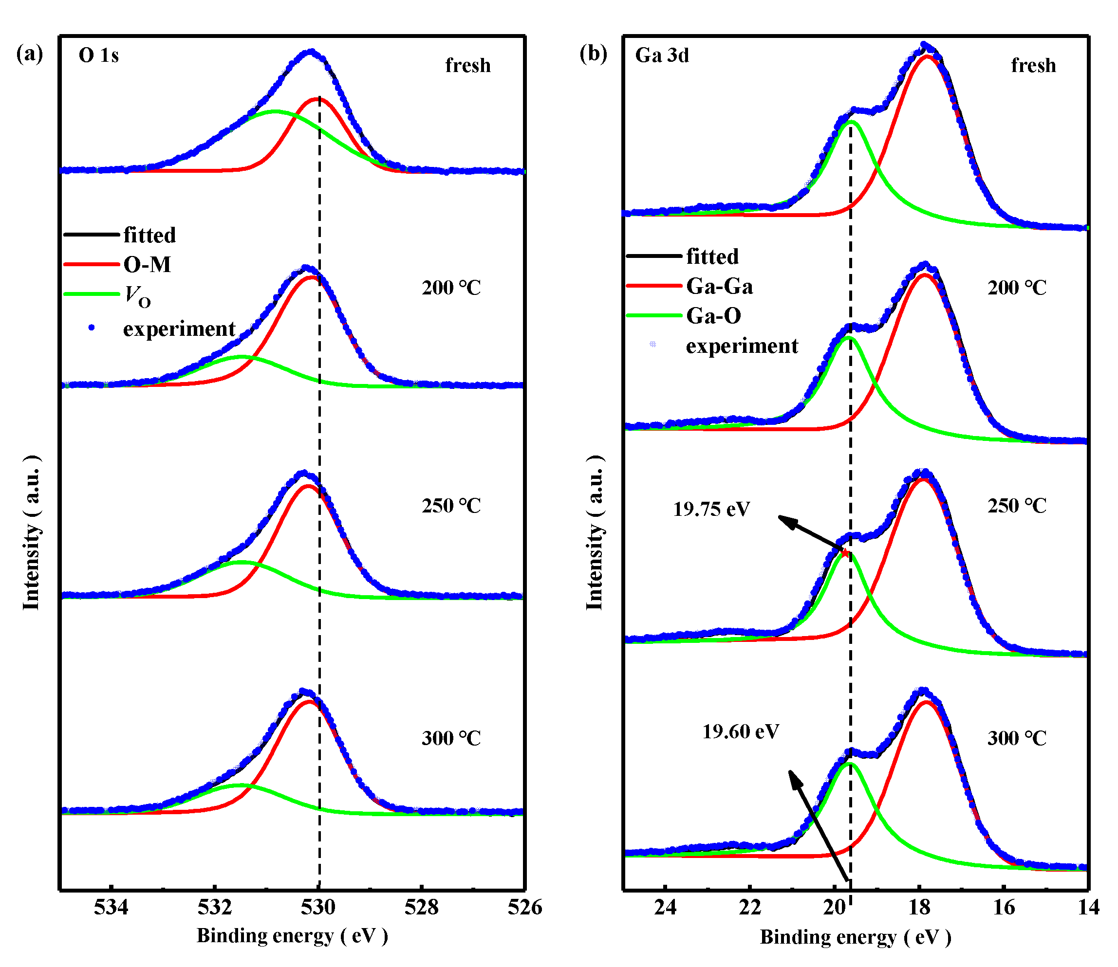
It is reported that the bonding states of gallium atoms in a-IGZO had a great impact on Vth, SS, and μ of a-IGZO TFTs [39,40]. It is known that the Ga-O bond exhibits the shortest bond length and the strongest binding energy compared to the In-O bond and Zn-O bond [30]. The XPS spectra of oxygen and gallium elements in a-IGZO films with first-annealing treatments at 200–300 °C were employed to investigate the relationship between transfer characteristics of TG-TFTs and the first-annealing temperature. The first-annealing temperature of the controlled samples were set at fresh (no first-annealing treatment), 200 °C, 250 °C, and 300 °C, respectively. Figure 7a,b showed the O 1s and Ga 3d XPS spectra of a-IGZO films with first-annealing treatments at fresh, 200 °C, 250 °C, and 300 °C, respectively. The O 1s spectra could be deconvoluted into two sub-peaks based on Gaussian fitting; i.e., the bond between O atom and metal atom (O-M) (centered around 530.15 eV) and VO (centered around 531.47 eV). The Ga 3d spectra could be deconvoluted into Ga-Ga (centered around 17.8 eV) and Ga-O (centered around 19.60 eV) [30,41,42,43]. The O-M core peaks of a-IGZO films with first-annealing at fresh, 200 °C, 250 °C, and 300 °C were at 530.02 eV, 530.12 eV, 530.20 eV, and 530.15 eV with an error of ±0.02 eV, while VO core peaks were at 530.85 eV, 531.45 eV, 531.55 eV, and 531.50 eV with an error of ±0.02 eV, respectively, as shown in Figure 6a. The core peak energy values of O-M for the a-IGZO films were almost consistent. The VO core peak energy for the a-IGZO film with first-annealing at 250 °C was found to be the biggest (531.55 eV), which indicated that the defect states in the a-IGZO film were located at the deepest energy level compared to that in other a-IGZO films, consistent with the PL spectra results from Figure 5. The contents of VO and O-M bonds were calculated from the O 1s spectra, as shown in Table 2. The VO contents in a-IGZO films were 26.60% (fresh), 11.17% (200 °C), 12.84% (250 °C), and 11.01% (300 °C), respectively. VO at shallow energy levels act as shallow donors, releasing electrons into the conduction band under the gate voltage; VO at deep energy levels would be ionized and capture electrons under the gate voltage field, leading to a decrease in mobility. For the IGZO film first-annealed at 250 °C, the VO content was higher than that in a-IGZO films first-annealed at 200 °C and 300 °C, as shown in Table 2. Additionally, PL spectra showed that the number of deep defects in the a-IGZO film first-annealed at 250 °C was greater than that in a-IGZO films first-annealed at 200 °C and 300 °C, as shown in Figure 5. Based on these two results, it suggested that the VO in the a-IGZO film first-annealed at 250 °C might occupy the central region of the bandgap, as shown in Figure 6c. The mobility of the 250 °C first-annealed TG-TFT decreased after a significant number of electrons were captured by the defects at the center of the bandgap under the gate voltage as shown in Table 1. On the other hand, the a-IGZO film first-annealed at 300 °C had a lower VO concentration compared to the a-IGZO film first-annealed at 200 °C, but these vacancies were mainly distributed at shallower energy levels below the conduction band. As shown in Figure 6d, the VO states occupying these shallow energy levels near the bottom of the conduction band released electrons into the conduction band under the gate voltage field, resulting in an increase in the carrier concentration and mobility. The contents of O-M bonds in a-IGZO films were 17.27% (fresh), 32.57% (200 °C), 30.45% (250 °C), and 32.44% (300 °C), respectively. The first-annealing treatment led to a 13.76–15.59% decrease in VO content and a 13.18–15.3% increase in the O-M bond content for a-IGZO films, as shown in Table 2. The change in the contents of VO and O-M bonds demonstrated that the O-related defects in a-IGZO films decreased with the first-annealing treatment temperature. The VO content in the 250 °C first-annealed a-IGZO film was slightly higher than that in a-IGZO films with first-annealing at 200 °C and 300 °C, indicating that the combination state between the O and metal atoms under this condition was different compared to other a-IGZO films.
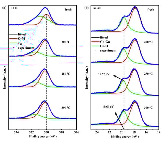
Figure 7.
(a) Deconvoluted O 1s XPS profile with VO and O-M, and (b) deconvoluted Ga 3d XPS profile with Ga-Ga and Ga-O in a-IGZO films received different first-annealing treatments at fresh, 200 °C, 250 °C, and 300 °C, respectively.
Table 2.
Bond content percentage of IGZO films with different first-annealing treatments.
In this report, the Ga-Ga peaks in all a-IGZO films were centered at 17.80 eV with a calculation error of ±0.02 eV. The Ga-O peak in the 250 °C first-annealed a-IGZO film was centered at 19.75 eV (Red star in Figure 7b), whereas the Ga-O peaks for other a-IGZO films were all centered at 19.60 eV with a calculation error of ±0.02 eV, as shown in Figure 7b. The 0.15 eV increase in the Ga-O peak indicated that the coordination between Ga and O in the 250 °C first-annealed a-IGZO film was better than that in other a-IGZO films. The Ga-O contents in a-IGZO films were 12.82% (fresh), 12.92% (200 °C), 11.18% (250 °C), and 13.34% (300 °C), respectively. The a-IGZO film with the first-annealing temperature at 300 °C had the highest Ga-O content. This might be the reason why TG TFTs with first-annealing at 300 °C exhibited the best PBS and NBS stability as shown in Figure 3c and Figure 4c, based on the fact that Ga-O could suppress the ionization of VO under gate bias [30].
Usually, an increase in VO in a-IGZO would lead to the Vth shifting in a negative direction, while the enhancement in the Ga-O bond would lead to the Vth shifting to positively. In comparison to the a-IGZO film with the first-annealing temperature at 200 °C, the 300 °C first-annealed a-IGZO film showed a 0.16% decrease in VO content and a 0.42% increase in Ga-O content. As a result, the Vth of the TG-TFT with the 300 °C first-annealed a-IGZO exhibited a positive shift. The VO content in the 250 °C first-annealed a-IGZO film was higher than that in the 200 °C and 300 °C annealed films, and while the Ga-O content in the 250 °C first-annealed a-IGZO film was lower than that in the 200 °C and 300 °C annealed films. Thus, the Vth of the TG-TFT with the 250 °C first-annealed a-IGZO should be more negative than that for the TG-TFTs with other a-IGZO films. However, the largest positive Vth was observed at the TG-TFT with the 250 °C first-annealed a-IGZO. This strange phenomenon might suggest that the Ga-O content had a greater impact on the Vth than VO content. And the better coordination between Ga and O promoted the idea that the Vth of the TG-TFT with the 250 °C first-annealed a-IGZO film was more positive than that for the 300 °C first-annealed TG-TFT.
4. Conclusions
In this work, the electrical properties and stabilities of a-IGZO TG-TFTs were systematically investigated by controlling the first-annealing temperature, and the mechanism of the first-annealing treatment on a-IGZO films was explored through PL spectra and XPS analysis. The TG-TFTs achieved good switching function when the first-annealing temperature at 200 °C–300 °C. The TG-TFT with the first-annealing treatment at 300 °C demonstrated the best electrical properties, PBS stability, and NBS stability.
The PL spectra and XPS spectra revealed the change in the O defect states and Ga-O bond state in the first-annealed a-IGZO films. O defects were reduced with first-annealing treatments, but some shallow states were produced when the first-annealing temperature increased to 300 °C. The best coordination situation between Ga and O atoms occurred for the a-IGZO film with the first-annealing treatment at 250 °C, leading to the biggest positive Vth of TG-TFTs. Furthermore, the highest content of the Ga-O bond and minimal defect intensity were both obtained in the a-IGZO film with first-annealing at 300 °C, which contributed to the excellent PBS and NBS stabilities of TG-TFTs. The interplay between O defects reduction and Ga-O bond strengthening underscores the importance of annealing temperature in balancing defect passivation and carrier transport for high-performance, transparent flexible electronics. This work provides a strategic framework for tailoring annealing processes to achieve highly stable a-IGZO TG-TFTs, advancing their applicability in next-generation transparent and wearable technologies.
Author Contributions
Experimental plan, S.Z.; verification, S.Z. and C.W.; investigation, S.Z., C.W. and S.L.; data processing, S.Z., L.D. and Z.L.; writing—first draft preparation, S.Z.; writing—review and editing, S.Z., Q.X., A.S., Y.L. and J.Z.; supervision, Y.L.; project management. Y.L. and J.Z. All authors have read and agreed to the published version of the manuscript.
Funding
This work was supported by Natural Science Foundation of Shandong Province (ZR2022ZD05, ZR2022ZD04, and ZR2020ZD03), National Key Research and Development Program of China (2022YFA1405200 and 2022YFB3603900), and National Natural Science Foundation of China (62074094).
Data Availability Statement
The data are contained within the article.
Conflicts of Interest
The authors declare no conflicts of interest.
References
- Kim, Y.; Jeon, G.J.; Lee, M.K.; Lee, S.H.; Park, S.H.K. Transparent top gate oxide TFT with ITO/Ag/ITO low resistance electrode for the application to the high speed operation fingerprint sensor array in the touch panel. In Proceedings of the 13th Symposium on Thin Film Transistor Technologies (TFT), Honolulu, HI, USA, 3–5 October 2016; pp. 247–251. [Google Scholar]
- Mativenga, M.; Haque, F. Highly Stable Thin-Film Transistors for Flexible and Transparent Displays. In Proceedings of the IEEE International Conference on Electrical, Computer, and Energy Technologies (ICECET), Cape Town, South Africa, 9–10 December 2021; pp. 2273–2278. [Google Scholar]
- Fan, J.; Chia-Yu, L.; Shu-jhih, C.; Liu Ming, G.; Zhang Li, J.; Sun, Y.; Lu Ma, C.; Xie Hua, F.; Liu, N.; Jianqing, S.; et al. High transparent Active matrix Mini-LED Full Color Display with IGZO TFT Backplane. SID Symp. Dig. Tech. Pap. 2019, 50, 454–456. [Google Scholar] [CrossRef]
- Li, Y.B.; Chen, T.P. Enhancement in Performance and Reliability of Transparent IGZO Thin-Film Transistors by ITO/Ti Stacked Source/Drain Contacts. ECS J. Solid State Sci. Technol. 2023, 12, 095003. [Google Scholar] [CrossRef]
- Li, J.; Zhang, Y.; Wang, J.; Yang, H.; Zhou, X.; Chan, M.; Wang, X.; Lu, L.; Zhang, S. Near-Ideal Top-Gate Controllability of InGaZnO Thin-Film Transistors by Suppressing Interface Defects with an Ultrathin Atomic Layer Deposited Gate Insulator. ACS Appl. Mater. Interfaces 2023, 15, 8666–8675. [Google Scholar] [CrossRef] [PubMed]
- Ning, H.; Zeng, X.; Zhang, H.; Zhang, X.; Yao, R.; Liu, X.; Luo, D.; Xu, Z.; Ye, Q.; Peng, J. Transparent Flexible IGZO Thin Film Transistors Fabricated at Room Temperature. Membranes 2022, 12, 29. [Google Scholar] [CrossRef] [PubMed]
- Kim, Y.-D.; Han, K.-L.; Kim, J.-H.; Lee, J.-I.; Lee, W.-B.; Park, J.-S.; Choi, B.-D. Effects of Tensile Strain on Dynamic and Static Inverters Using Amorphous Indium-Gallium-Zinc-Oxide TFTs. IEEE Electron Device Lett. 2021, 42, 359–362. [Google Scholar] [CrossRef]
- Velichko, R.; Magari, Y.; Furuta, M. Defect Passivation and Carrier Reduction Mechanisms in Hydrogen-Doped In-Ga-Zn-O (IGZO:H) Films upon Low-Temperature Annealing for Flexible Device Applications. Materials 2022, 15, 334. [Google Scholar] [CrossRef]
- Hanyu, Y.; Abe, K.; Domen, K.; Nomura, K.; Hiramatsu, H.; Kumomi, H.; Hosono, H.; Kamiya, T. Effects of High-Temperature Annealing on Operation Characteristics of a-In-Ga-Zn-O TFTs. J. Disp. Technol. 2014, 10, 979–983. [Google Scholar] [CrossRef]
- Oka, N.; Aoi, T.; Hayashi, R.; Kumomi, H.; Shigesato, Y. Electronic State of Amorphous Indium Gallium Zinc Oxide Films Deposited by DC Magnetron Sputtering with Water Vapor Introduction. Appl. Phys. Express 2012, 5, 075802. [Google Scholar] [CrossRef]
- Zhang, W.; Fan, Z.; Shen, A.; Dong, C. Atmosphere Effect in Post-Annealing Treatments for Amorphous InGaZnO Thin-Film Transistors with SiOx Passivation Layers. Micromachines 2021, 12, 1551. [Google Scholar] [CrossRef]
- Kang, D.H.; Kang, I.; Ryu, S.H.; Ahn, Y.S.; Jang, J. Effect of SiO2 and/or SiNX Passivation Layer on Thermal Stability of Self-Aligned Coplanar Amorphous Indium-Gallium-Zinc-Oxide Thin-Film Transistors. J. Disp. Technol. 2013, 9, 699–703. [Google Scholar] [CrossRef]
- Hsieh, H.-H.; Kamiya, T.; Nomura, K.; Hosono, H.; Wu, C.-C. Modeling of amorphous InGaZnO4 thin film transistors and their subgap density of states. Appl. Phys. Lett. 2008, 92, 133503. [Google Scholar] [CrossRef]
- Chen, W.-T.; Lo, S.-Y.; Kao, S.-C.; Zan, H.-W.; Tsai, C.-C.; Lin, J.-H.; Fang, C.-H.; Lee, C.-C. Oxygen-Dependent Instability and Annealing/Passivation Effects in Amorphous In-Ga-ZnO Thin-Film Transistors. IEEE Electron Device Lett. 2011, 32, 1552–1554. [Google Scholar] [CrossRef]
- Aman, S.G.M.; Magari, Y.; Shimpo, K.; Hirota, Y.; Makino, H.; Koretomo, D.; Furuta, M. Low-temperature (150 °C) activation of Ar+O2+H2-sputtered In-Ga-Zn-O for thin-film transistors. Appl. Phys. Express 2018, 11, 081101. [Google Scholar] [CrossRef]
- Zheng, S.; Lv, S.; Wang, C.; Li, Z.; Dong, L.; Xin, Q.; Song, A.; Zhang, J.; Li, Y. Post-annealing effect of low temperature atomic layer deposited Al2O3 on the top gate IGZO TFT. Nanotechnology 2024, 35, 155203. [Google Scholar] [CrossRef]
- Nomura, K.; Kamiya, T.; Ohta, H.; Hirano, M.; Hosono, H. Defect passivation and homogenization of amorphous oxide thin-film transistor by wet O2 annealing. Appl. Phys. Lett. 2008, 93, 192107. [Google Scholar] [CrossRef]
- Lee, H.-W.; Cho, W.-J. Effects of vacuum rapid thermal annealing on the electrical characteristics of amorphous indium gallium zinc oxide thin films. AIP Adv. 2018, 8, 015007. [Google Scholar] [CrossRef]
- Thi Thu Thuy, N.; Aventurier, B.; Renault, O.; Terlier, T.; Barnes, J.P.; Templier, F. Impact of hydrogen diffusion on electrical characteristics of IGZO TFTs passivated by SiO2 or Al2O3. In Proceedings of the 21st International Workshop on Active-Matrix Flatpanel Displays and Devices-TFT Technologies and FPD Materials (AM-FPD), Kyoto, Japan, 2–4 July 2014; pp. 149–152. [Google Scholar]
- Wang, C.; Zeng, C.; Ning, H.; Li, F.; Liu, M.; Xu, K.; Ma, F. Enhanced performances of a-IGZO TFTs with oxide passivation layers fabricated by hollow cathode assisted PLD. J. Alloys Compd. 2023, 961, 170972. [Google Scholar] [CrossRef]
- Peng, C.; Yang, S.; Pan, C.; Li, X.; Zhang, J. Effect of Two-Step Annealing on High Stability of a-IGZO Thin-Film Transistor. IEEE Trans. Electron Devices 2020, 67, 4262–4268. [Google Scholar] [CrossRef]
- Li, J.; Zhang, Y.; Wang, J.; Yang, H.; Zhou, X.; Chan, M.; Wang, X.; Lu, L.; Zhang, S. High-Performance Self-Aligned Top-Gate Amorphous InGaZnO TFTs With 4 nm-Thick Atomic-Layer-Deposited AlOX Insulator. IEEE Electron Device Lett. 2022, 43, 729–732. [Google Scholar] [CrossRef]
- Lim, J.S.; Yam, F.K. Influence of thermal treatment duration on the morphological and optical properties of a-IGZO. J. Mater. Sci.-Mater. Electron. 2023, 34, 1302. [Google Scholar] [CrossRef]
- Yokoyama, M.; Asakura, Y.; Yokoyama, H.; Takenaka, M.; Takagi, S. Impact of Al2O3 ALD temperature on Al2O3/GaSb metal-oxide-semiconductor interface properties. In Proceedings of the 2013 International Conference on Indium Phosphide and Related Materials, Kobe, Japan, 19–23 May 2013; IEEE: New York, NY, USA, 2013; p. 6132. [Google Scholar]
- Ma, P.; Du, L.; Wang, Y.; Jiang, R.; Xin, Q.; Li, Y.; Song, A. Low voltage operation of IGZO thin film transistors enabled by ultrathin Al2O3 gate dielectric. Appl. Phys. Lett. 2018, 112, 023501. [Google Scholar] [CrossRef]
- Tsao, S.W.; Chang, T.C.; Huang, S.Y.; Chen, M.C.; Chen, S.C.; Tsai, C.T.; Kuo, Y.J.; Chen, Y.C.; Wu, W.C. Hydrogen-induced improvements in electrical characteristics of a-IGZO thin-film transistors. Solid·State Electron. 2010, 54, 1497–1499. [Google Scholar] [CrossRef]
- Chang, Y.-H.; Yu, M.-J.; Lin, R.-P.; Hsu, C.-P.; Hou, T.-H. Abnormal positive bias stress instability of InGaZnO thin-film transistors with low-temperature Al2O3 gate dielectric. Appl. Phys. Lett. 2016, 108, 033502. [Google Scholar] [CrossRef]
- Jang, J.T.; Ko, D.; Choi, S.-J.; Kim, D.M.; Kim, D.H. Observation of Hydrogen-Related Defect in Subgap Density of States and Its Effects Under Positive Bias Stress in Amorphous InGaZnO TFT. IEEE Electron Device Lett. 2021, 42, 708–711. [Google Scholar] [CrossRef]
- Chien, Y.-T.; Tsai, Y.-L.; Zhou, K.-J.; Zheng, Y.-Z.; Tai, M.-C.; Tu, H.-Y.; Kuo, C.-W.; Chang, T.-C.; Tsai, T.-M. Performance Enhancement of InGaZnO Top-Gate Thin Film Transistor With Low-Temperature High-Pressure Fluorine Treatment. IEEE Electron Device Lett. 2021, 42, 1611–1614. [Google Scholar] [CrossRef]
- Noh, H.-K.; Chang, K.J.; Ryu, B.; Lee, W.-J. Electronic structure of oxygen-vacancy defects in amorphous In-Ga-Zn-O semiconductors. Phys. Rev. B 2011, 84, 115205. [Google Scholar] [CrossRef]
- Samanta, C.; Yuvaraja, S.; Zhama, T.; Zhao, H.; Gundlach, L.; Zeng, Y. High-Performance TiO2 Thin-Film Transistors: In-Depth Investigation of the Correlation between Interface Traps and Oxygen Vacancies. ACS Appl. Electron. Mater. 2024, 6, 5575–5585. [Google Scholar] [CrossRef]
- Avis, C.; Jang, J. Understanding the Origin of the Hysteresis of High-Performance Solution Processed Polycrystalline SnO2 Thin-Film Transistors and Applications to Circuits. Membranes 2022, 12, 7. [Google Scholar] [CrossRef]
- Morimoto, T.; Yang, Y.; Ochiai, Y.; Fukuda, N.; Ohki, Y. Effects of metal content on electrical and physical properties in solution-processed IGZO thin films. Appl. Phys. A-Mater. Sci. Process. 2020, 126, 388. [Google Scholar] [CrossRef]
- Jeong, S.H.; Bae, B.S.; Yu, K.M.; Ryu, M.K.; Cho, K.I.; Yun, E.-J. Properties of IGZO thin films irradiated by electron beams with various energies. J. Korean Phys. Soc. 2012, 61, 867–872. [Google Scholar] [CrossRef]
- Hino, A.; Kishi, T.; Morita, S.; Hayashi, K.; Kugimiya, T. Study of electronic structure and composition at back channel surface of amorphous In-Ga-Zn-O thin films. In Proceedings of the 11th Symposium on Thin Film Transistor Technologies (TFT), Honolulu, HI, USA, 8–10 October 2012; pp. 197–202. [Google Scholar]
- Takamori, Y.; Morimoto, T.; Fukuda, N.; Ohki, Y. Effects of ultraviolet photon irradiation and subsequent thermal treatments on solution-processed amorphous indium gallium zinc oxide thin films. AIP Adv. 2018, 8, 115304. [Google Scholar] [CrossRef]
- Yu, E.K.-H.; Jun, S.; Kim, D.H.; Kanicki, J. Density of states of amorphous In-Ga-Zn-O from electrical and optical characterization. J. Appl. Phys. 2014, 116, 154505. [Google Scholar] [CrossRef]
- Pu, H.; Zhou, Q.; Yue, L.; Zhang, Q. Investigation of oxygen plasma treatment on the device performance of solution-processed a-IGZO thin film transistors. Appl. Surf. Sci. 2013, 283, 722–726. [Google Scholar] [CrossRef]
- Zhang, Y.Y.; Qian, L.X.; Ge, W.B.; Lai, P.T.; Liu, X.Z. Tailoring the Band Alignment of GaxZn1−xO/InGaZnO Heterojunction for Modulation-Doped Transistor Applications. Phys. Status Solidi A-Appl. Mater. Sci. 2018, 215, 180032. [Google Scholar] [CrossRef]
- Seo, Y.-J.; Lee, J.-W.; Kwon, Y.-H.; Seong, N.-J.; Choi, K.-J.; Yoon, S.-M. Synergistic Effects of Deposition Temperatures for Active and Gate Insulator of Top-Gate Thin-Film Transistors Using InGaZnO Channels Prepared by Thermal Atomic-Layer Deposition. ACS Appl. Electron. Mater. 2024, 6, 7563–7575. [Google Scholar] [CrossRef]
- Kim, C.-K.; Kim, E.; Lee, M.K.; Park, J.-Y.; Seol, M.-L.; Bae, H.; Bang, T.; Jeon, S.-B.; Jun, S.; Park, S.-h.K.; et al. Electrothermal Annealing (ETA) Method to Enhance the Electrical Performance of Amorphous-Oxide-Semiconductor (AOS) Thin-Film Transistors (TFTs). ACS Appl. Mater. Interfaces 2016, 8, 23820–23826. [Google Scholar] [CrossRef]
- Xie, H.; Zhou, Y.; Zhang, Y.; Dong, C. Chemical bonds in nitrogen-doped amorphous InGaZnO thin film transistors. Results Phys. 2018, 11, 1080–1086. [Google Scholar] [CrossRef]
- Kishore, R.; Vishwakarma, K.; Datta, A. Effect of Non-identical Annealing on the Breakdown Characteristics of Sputtered IGZO Films. In Proceedings of the 2022 IEEE International Reliability Physics Symposium (IRPS), Dallas, TX, USA, 27–31 March 2022; pp. P24-1–P24-4. [Google Scholar] [CrossRef]
Disclaimer/Publisher’s Note: The statements, opinions and data contained in all publications are solely those of the individual author(s) and contributor(s) and not of MDPI and/or the editor(s). MDPI and/or the editor(s) disclaim responsibility for any injury to people or property resulting from any ideas, methods, instructions or products referred to in the content. |
© 2025 by the authors. Licensee MDPI, Basel, Switzerland. This article is an open access article distributed under the terms and conditions of the Creative Commons Attribution (CC BY) license (https://creativecommons.org/licenses/by/4.0/).