Article

Enhanced Optoelectronic Response of TiO2 Photodetector Sensitized via CuInSe2 Quantum Dots

1
Shandong Engineering Research Center of New Optoelectronic Information Technology and Devices, School of Mathematics and Physics, Qingdao University of Science & Technology, Qingdao 266061, China
2
School of Physics and Technology, University of Jinan, Jinan 250022, China
*
Authors to whom correspondence should be addressed.
Nanomaterials 2025, 15(7), 522; https://doi.org/10.3390/nano15070522
Submission received: 2 March 2025 / Revised: 28 March 2025 / Accepted: 28 March 2025 / Published: 30 March 2025

Abstract

:
Colloidal copper-based chalcogenide quantum dots (QDs), particularly lead-free CuInSe2 systems, have emerged as promising photosensitizers for optoelectronic de-vices due to their high extinction coefficients and solution processability. In this work, we demonstrate a TiO2 photodetector enhanced through interfacial engineering with the size of 9.88 ± 2.49 nm CuInSe2 QDs, synthesized via controlled thermal injection. The optimized device architecture combines a 160 nm TiO2 active layer with 60 μm horizontal channel electrodes, achieving high performance metrics. The QD-sensitized device demonstrates an impressive switching ratio of approximately 105 in the 405 nm wavelength, a significant 34-times increase in responsivity at a 2 V bias, and a detection rate of 4.17 × 10⁸ Jones. Due to the limitations imposed by the TiO2 bandgap, the TiO2 photodetector exhibits a negligible increase in photocurrent at 565 nm. The engineered type-II heterostructure enables responsivity enhancement across an extended spectral range through sensitization while maintaining equivalent performance characteristics at both 405 nm and 565 nm wavelengths. Furthermore, the sensitized architecture demonstrates superior response kinetics, enhanced specific detectivity, and exceptional operational stability, establishing a universal design framework for broadband photodetection systems.

1. Introduction

With the rapid advancement of information technology and the growing demand for high-speed communication, optical sensors, and imaging technologies, photodetectors have become essential components in modern technological applications [1,2]. Conventional photodetectors, particularly those based on semiconductor materials like titanium dioxide (TiO2) [3], are extensively utilized across various fields due to their low cost, stability, and excellent chemical properties [4,5,6,7]. However, the application of TiO2 in photodetectors still faces some challenges, especially in terms of photoelectric conversion efficiency and optical response range. The large bandgap of TiO2 leads to its low absorption efficiency in the visible range, limiting its performance in low-light detection and multi-band response. To overcome this problem, Chen et al. prepared photoelectrochemical-based photodetectors based on Cu2O/TiO2 heterostructures with a special interfacial structure that accelerates the separation and transfer of photogenerated carriers [8]. Yang et al. prepared photodetectors based on TiO2/Bi2Se3 heterostructures, which fully utilize the light-absorbing properties of TiO2 to absorb more photons and generate larger photocurrents [9]. Whereas the approach of simply constructing a heterojunction has enhanced photocurrent, responsivity, and detection rate [10], there will still be a limitation on the photoresponse detection range. The work reported by Govind Gupta et al. provides an up-to-date perspective on how TiO2 can be structurally and electronically modified for improved device applications. By integrating these insights, our study further explores the synergistic effects of quantum dot sensitization and TiO2 modification, providing a new avenue for optimizing photodetector performance. Based on the unique photovoltaic properties of quantum dots (QDs) [11] high extinction coefficient, tunable bandgap, and excellent photovoltaic conversion efficiency, photons can be effectively captured and more electron-hole pairs can be generated, which can improve the responsivity and detection rate of photodetectors. Rajeev Ray et al. constructed an improved photodetector using chalcogenide QDs and atomic layer deposition (ALD) ultrathin TiO2 films to enhance the overall performance of heterostructures photodetectors through interface engineering [12]. Qu et al. investigated Ag NPs and MoS2 QDs dual-modified graphene/gallium arsenide near-infrared photodetectors, utilizing the dielectric confinement effect of MoS2 QDs to enhance the performance of the photodetectors [13]. The unique quantum effect of QDs makes them another effective strategy to broaden the detectable band [14], and lead-free colloidal copper-based sulfur-based QDs (e.g., CuInSe2 QDs) have been widely used in optoelectronics by virtue of their low cost, lower risk of environmental contamination, and tunable bandgap [15,16]. The bandgap of CuInSe2 QDs is highly tunable, which enables them to perform effective photovoltaic responses in different spectral ranges, especially for the absorption of near-infrared (NIR) light [17,18]. In addition, more mature synthesis methods for CuInSe2 QDs, such as thermal injection, are capable of synthesizing QDs with excellent optoelectronic properties, whose size and morphology can be precisely adjusted by controlling the synthesis conditions. These excellent photovoltaic properties make CuInSe2 QDs ideal photodetector materials [16,19,20,21], which can significantly enhance the performance of conventional photovoltaic materials such as TiO2.
In this study, CuInSe2 QDs with an average size of ~9.88 nm were synthesized by thermal injection and applied to sensitization optimizing of TiO2 photodetectors. At 405 nm, the responsivity (R) and detectivity (D*) reached 4.44 × 10⁻⁵ mA/W and 4.17 × 10⁸ Jones. Moreover, the type-II heterostructure, which extends the detectable range to 565 nm, enables the sensitized photodetectors to exhibit significant improvements in responsivity and detectivity, highlighting the great potential of CuInSe2 QDs as a sensitizing material for TiO2 photodetectors. This work is distinctive in that it exploits the advantages of CuInSe2 QD sensitization and self-powered behavior while addressing the major limitations identified in previous studies, contributing to the continued development of high-performance, environmentally sustainable optoelectronic devices based on QDs—TiO2 heterostructures.

2. Materials and Methods

CuInSe2 QDs were synthesized using the thermal injection method. The Se-TOP precursor was prepared by dissolving selenium powder in tri-n-octylphosphine (TOP), followed by sonication for 60 min. The resulting solution was then maintained at 120 °C. CuI and In(C2H3O2)3 were placed in a three-necked flask, followed by the addition of the reducing agent oleylamine (OLA) and 1-octadecene (ODE). Nitrogen was introduced to purge the system for 5 min at room temperature. The mixture was then heated to 170 °C and maintained at this temperature for 10 min. Subsequently, the Se-TOP precursor solution was injected into the flask over 3 min. The reaction was quenched by an ice-water bath, and methanol was added to perform three rounds of suspension precipitation. Finally, the precipitate was dispersed in toluene to obtain CuInSe2 QDs [22].
An N-doped single-sided silicon oxide wafer was used as the substrate, on which a TiO2 electron transport layer was deposited via electron beam evaporation and annealed at 600 °C for 40 min. TiO2 photodetectors were fabricated by placing a mask plate on the TiO2 thin film layer, followed by sequential electron beam deposition of Au/Ti to preparate the electrodes. CuInSe2 QDs were spin-coated onto the TiO2 photodetectors. A volume of 80 μL of the QDs solution was applied, and the substrates were spun at 2500 rpm for 30 s. This process was repeated five times with a 20 s interval between each deposition, and the devices were then dried for 15 min at 80 °C to complete the preparation.
The materials required for the experiment are listed below: 1-Octadecene(ODE, >90%), oleylamine(OLA, 80–90%), Tri-n-octylphosphine (TOP, 90%), Selenium (Se, 99.9%), Indium acetate (In(C2H3O2)3, 99.99%), cuprous iodide (CuI, 99.9%), methanol (CH3OH, 99.5%), n-hexane (C6H14, 97%) purchased from Shanghai McLean Biochemical Co., Ltd. (Shanghai, China). TiO2 Pellets, Ti Pellets, Au Pellets purchased from Zhongnuo New Material (Beijing) Technology Co., Ltd. (Beijing, China). Single-sided oxidized silicon wafers were purchased from Suzhou Crystal Silicon Electronic Technology Co., Ltd. (Suzhou, China).

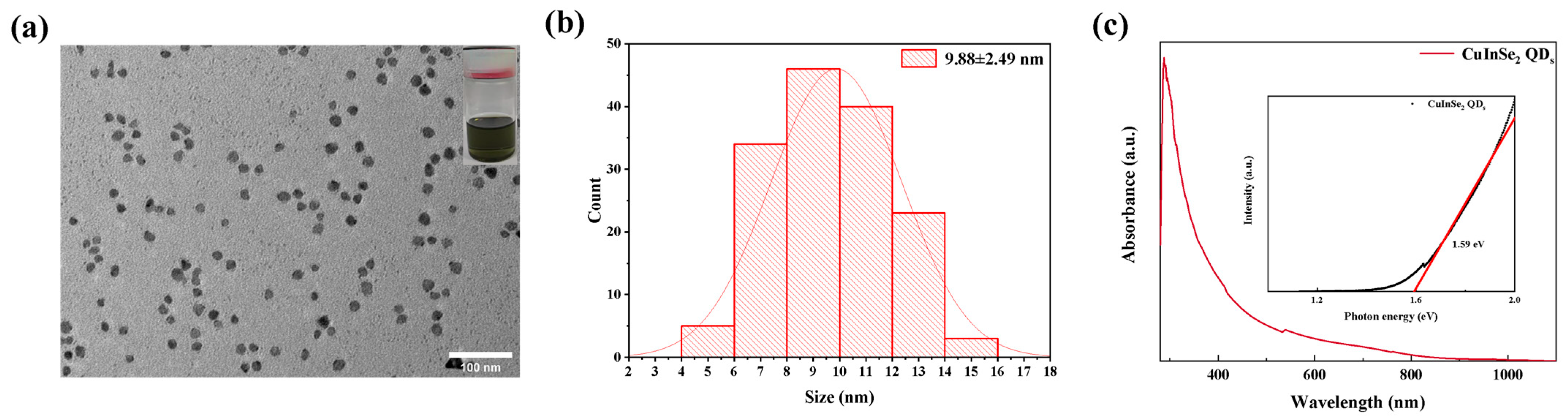
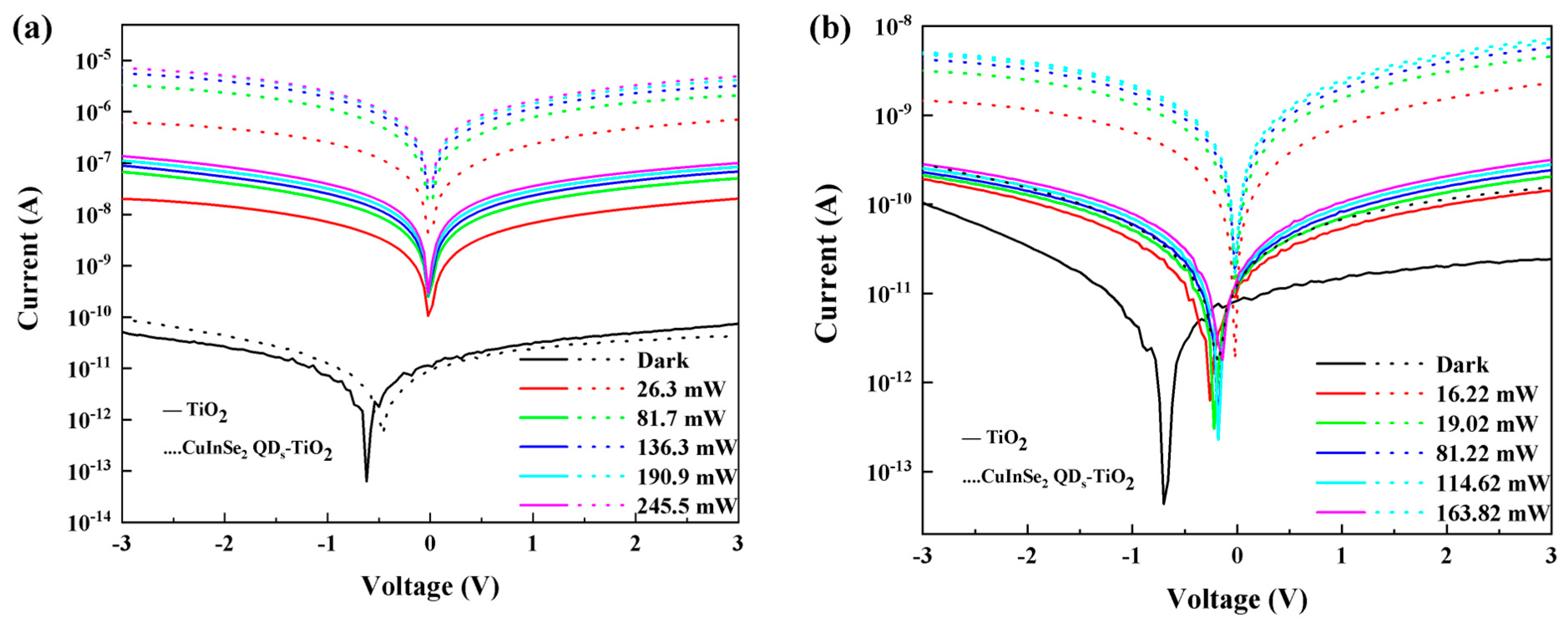
3. Results and Discussions

The synthesized CuInSe2 QDs were characterized, and Figure 1a,b present the TEM images and particle size distribution of the CuInSe2 QDs. The morphology of the QDs is an approximately circular shape, with an average size of ~9.88 nm, which is smaller than the 10.6 nm Bohr exciton radius of CuInSe2 QDs [16]. Figure 1c shows the absorption spectrum of CuInSe2 QDs, with a range from 280 to 1100 nm; the strongest absorption peak occurs at ~300 nm, and the band gap of CuInSe2 QDs was calculated to be 1.59 eV according to the Tauc Plot method.
Figure 2a depicts the cross-sectional architecture of the sensitized device, where a uniform monolayer of CuInSe2 QDs is assembled on the mesoporous TiO2 electron-transport layer (ETL) through optimized spin-coating processing. In this configuration, the CuInSe2 QD layer functions as the primary photoactive component, achieving effective photon capture across visible to near-infrared spectra, while the underlying TiO2 scaffold serves dual functions: (i) facilitating rapid electron extraction from the QDs through its tailored conduction band alignment and (ii) providing a continuous 3D charge transport network with minimized recombination losses. Figure 2b presents a representative AFM topography image of the sensitized device, revealing key morphological characteristics of the spin-coated CuInSe2 QDs/TiO2 heterostructure. Quantitative analysis shows that the root mean square roughness of the CuInSe2 QD-modified surface is 1.26 nm; the maximum height roughness is 14 nm, which is a 40% increase compared to the bare TiO2 substrate (10 nm). This controlled roughening demonstrates uniform QDs coverage while maintaining nanoscale ordering, and the spin-coated QDs mask some of the defective states, which makes the surface of the film denser. A moderate amount of roughness enhances the interfacial contact between TiO2 and CuInSe2 quantum dots, which promotes charge transfer, and the increase in surface roughness also leads to an increase in the effective area, which promotes better light absorption and reduces reflective losses, as well as generating localized surface defects, which serve as charge trapping centers and increase recombination [23]. Figure 2c shows the XRD patterns of the TiO2 layer. The figure shows several characteristic peaks which correspond to the Ref. [24], with the strongest peak at 2θ = 27.4°, corresponding to the 110 crystal plane, which exhibits a rutile phase [24]. Calculations based on Scherrer’s formula with the Williamson–Hall model [25] show that TiO2 films prepared by electron beam evaporation have a large grain size (59.76 nm), a low dislocation density (2.8 × 10¹³ m−2), and a small strain (0.018%), which is superior to that of typical sol-gel processes. Grain size optimization significantly reduces grain boundary scattering, and the combination of low defect density and lattice integrity synergistically improves carrier mobility and device stability. Figure 2d shows the absorption spectrum of TiO2 with the absorption peak at 350 nm, and the band gap of TiO2 was calculated to be 2.58 eV according to the Tauc Plot method, which directly affects its photoresponse in the visible wavelength band due to its forbidden band width [26,27]. This can also be verified from the photocurrents we tested on simple TiO2 photodetectors in the 565 nm band.
Figure 3a,b show the IV output characteristics of TiO2 photodetectors versus TiO2 photodetectors enhanced by sensitization of CuInSe2 QDs under the illumination of LEDs of different powers at 405 nm and 565 nm. The devices before and after sensitization show typical bipolar characteristics, especially the “V”-shaped transfer curves, which show the transfer of electrons or holes in the n-type or p-type channels of the devices, respectively, and the sensitized photocurrent exhibits a significant enhancement. For the self-powered behavior of the device, we calculated the open-circuit voltage Voc and short-circuit current Isc of the CuInSe2 QD-sensitized TiO2 photodetector at 405 nm illumination, which are 0.001 V and 4.62 × 10⁻¹⁰ A, respectively. The self-powered characteristics of the constructed device based on the heterostructure of CuInSe2 QDs/TiO2 were verified [28]. The switching ratio is the ratio of light current to dark current, as can be seen in Figure 3a; the sensitized device achieves a high switching ratio of about 105 at a 405 nm wavelength with a 3 V bias voltage of 245.5 mW, and the photocurrent increases with the increase in optical power. In Figure 3b, it can be seen that the photocurrent of the TiO2 photodetector at the 565 nm wavelength does not show significant growth with the increase in optical power, and the photocurrent shows a saturated state. The response of the device to light is significantly enhanced after sensitization with CuInSe2 QDs, allowing a detectable range up to 565 nm. In addition, the surface defects of CuInSe2 QDs can quench any small current under dark conditions. Under light illumination, the photocarriers generated in CuInSe2 QDs can rapidly fill the defects in the quantum dots, which can effectively collect the photocurrents in the thin films that are mainly generated by the TiO2 component [20].
A type-II heterostructure between CuInSe2 QDs and TiO2 is attributed to the improvement in photoresponsive properties [29]. The valence band offset between the CuInSe2 QDs and TiO2 is 1.42 eV. In addition, the conduction band offset calculated using the VBM and the bandgap of the two materials obtained by Tauc Plot fitting was determined to be about 0.41 eV [28]. According to the energy band theory, photogenerated electrons are spontaneously injected from the conduction band bottom of CuInSe2 QDs into the conduction band bottom of TiO2, forming an energy level difference as a thermodynamic driving force, which causes the electrons to rapidly detach from the quantum dot interface and migrate to the external circuit. As shown in Figure 4, the photogenerated holes at the top of the TiO₂ valence band are transferred to the top of the valence band of CuInSe2 QDs through the assistance of the interface’s built-in electric field, and the migration process is accelerated by the localized electric field formed by the bending of the energy bands inside the heterojunction [22,30]. This charge separation mechanism significantly reduces the compounding probability of electron-hole pairs and extends the carrier lifetime, thereby enhancing the photocurrent density. The energy band shift at the interface of the type-II heterojunction induces the formation of a built-in electric field (in the direction from CuInSe2 QDs to TiO2), which further facilitates the injection efficiency of photogenerated electrons into the conduction band of TiO2 and at the same time drives the migration of holes into the valence band of the CuInSe2 QDs to realize the fast spatial separation of carriers.
The responsivity (R) is one of the key parameters of a photodetector, defined as the photocurrent generated per unit of effective incident power, and R can be calculated from Equation (1):
R = Δ I D S P = I i l l u I d a r k E e × S
where Iillu is the generated photocurrent, P is the optical power density, Ee is the optical power density, and S is the effective area of the photosensitive region. The responsivity changes corresponding to the different optical powers of the two devices were calculated at a bias voltage of 3 V, as shown in Figure 5. The sensitized devices at both wavelengths show a significant increase in responsiveness compared to the original devices. Figure 5a shows the plot of R versus optical power at a wavelength of 405 nm. R reaches 4.44 × 10⁻⁵ mA/W at an optical power density of 13.1 mW/cm2. The sensitized responsivity is improved by 34 times over the 1.28 × 10⁻⁶ mA/W of the TiO2 device alone. Figure 5b represents the plot of R with optical power at a 565 nm wavelength, where the responsivity reaches 2.16 × 10⁻⁷ mA/W at an optical power density of 8.07 mW/cm2. Responsivity decreases with increasing light intensity; this dependence can be attributed to several factors, with a gradual decrease in responsivity due to enhanced carrier complexation and gradual saturation of the photocurrent [31,32]. At low light intensities, the trap state traps a large fraction of the photogenerated electrons, thus reducing the recombination of electron-hole pairs [33]. Conversely, at higher light intensities, heating effects and sensitized trap saturation in the quantum dots may also lead to reduced responsivity, including heterostructures and defects within their interfaces, and the availability of trap states that capture photogenerated electrons is relatively limited. As a result, the device is more responsive at lower light intensities [34].
Another key parameter characterizing the performance of the photodetector is the specific detectivity D*, which can be calculated by Equation (2) [35]:
D * = R A 1 / 2 ( 2 e I d s ) 1 / 2
where R is the responsivity, A is the area of the detector, e is the charge of an electron, and Ids is the dark current. The variation curve of D* with optical power at 2 V bias voltage is shown in Figure 5. Figure 5c represents the variation curve of detectivity with optical power density at 405 nm wavelength, and the detectivity of the sensitized device reaches 4.17 × 10⁸ Jones at a power density of 13.1 mW/cm2. Figure 5d represents the variation curve of detectivity with optical power density at a 565 nm wavelength; the D* at a 565 nm wavelength decreases with the increase in optical power density, showing the same behavior as the responsivity. The highest detection rate reaches 9.54 × 10⁵ Jones, which indicates that the device is more sensitive to the detection of weak light. The NEP is the least detectable power density for the dark noise by a PD with a 1 Hz bandwidth frequency and can be defined as [36].
N E P = 2 e × I d s R
The NEP of the sensitized device at 3 V bias voltage (405 nm) was calculated and reached up to 9.49 × 10⁻¹¹ W/Hz.

4. Conclusions

CuInSe2 QDs with an average size of 9.88 ± 2.49 nm were synthesized using the solution-phase synthesis method, and the TiO2-based photodetectors sensitized by the CuInSe2 QDs were prepared. The optimized device architecture synergized with QD-induced interfacial band engineering, achieving remarkable performance enhancement. The maximum switching ratio reached 105 in the 405 nm band, and the responsivity reached 4.44 × 10⁻⁵ mA/W, a 34-times improvement over simple TiO2 devices. The detectivity reached 4.17 × 10⁸ Jones at 405 nm. The sensitized responsivity and detectivity exhibit the same photoresponse enhancement behavior, effectively allowing a detectable wavelength up to 565 nm. Thus, solution-based, low-cost processes and device performance enhancement make lead-free CuInSe2 QDs promising materials for self-powered optoelectronic applications, and sensitization through quantum dots has become an effective method for photodetector performance enhancement.

Author Contributions

Conceptualization, Y.Z.; methodology, K.Y.; validation, M.L. and S.X.; formal analysis, X.D.; investigation, Y.Z.; data curation, Y.Z. and K.Y.; writing—original draft preparation, Y.Z.; writing—review and editing, M.W. and Q.Z.; visualization, J.Z. and Y.Z.; supervision, M.W.; project administration, X.W.; funding acquisition, X.W. All authors have read and agreed to the published version of the manuscript.

Funding

This work is supported by the National Natural Science Foundation of China (Nos.12174211, 11874232, 12174212).

Data Availability Statement

Data underlying the results presented in this paper are not publicly available at this time but may be obtained from the authors upon reasonable request.

Acknowledgments

Thanks for the support of the Youth Innovation team.

Conflicts of Interest

The authors declare no conflicts of interest.

References

  1. Tang, X.; Yang, J.; Duan, Z.; Bu, Y.; Yuan, Z.; Jiang, Y.; Tai, H. Advances in Paper-Based Photodetectors: Fabrications, Performances, and Applications. Adv. Opt. Mater. 2024, 12, 2401114. [Google Scholar] [CrossRef]
  2. Koppens, F.H.; Mueller, T.; Avouris, P.; Ferrari, A.C.; Vitiello, M.S.; Polini, M. Photodetectors based on graphene, other two-dimensional materials and hybrid systems. Nat. Nanotechnol. 2014, 9, 780–793. [Google Scholar] [CrossRef] [PubMed]
  3. Hazra, S.; Singh, S.V.; Dahiya, S.; Aich, P.K.; Pal, B.N. Solution-Processed Ag-TiO2 Nanostructure-Based Schottky Junction Thin Films for Narrowband Hot-Electron Photodetectors. ACS Appl. Nano Mater. 2023, 6, 15119–15127. [Google Scholar] [CrossRef]
  4. Ibrahem, M.A.; Verrelli, E.; Adawi, A.M.; Bouillard, J.G.; O’Neill, M. Plasmons Enhancing Sub-Bandgap Photoconductivity in TiO2 Nanoparticles Film. ACS Omega 2024, 9, 10169–10176. [Google Scholar] [CrossRef] [PubMed]
  5. Kaawash, N.M.S.; Halge, D.I.; Narwade, V.N.; Khanzode, P.M.; Thabit, M.Y.H.; Begum, A.; Shaikh, S.J.; Dadge, J.W.; Alegaonkar, P.S.; Bogle, K.A. Unconventional Enhancement of UV Photodetection in Surface-Passivated TiO2 Thin Film Photodetectors. ACS Appl. Eng. Mater. 2023, 1, 3368–3378. [Google Scholar] [CrossRef]
  6. Kunwar, S.; Pandit, S.; Kulkarni, R.; Mandavkar, R.; Lin, S.; Li, M.Y.; Lee, J. Hybrid Device Architecture Using Plasmonic Nanoparticles, Graphene Quantum Dots, and Titanium Dioxide for UV Photodetectors. ACS Appl. Mater. Interfaces 2021, 13, 3408–3418. [Google Scholar] [CrossRef]
  7. Kwon, Y.; Kim, H.; Lee, S.; Chin, I.-J.; Seong, T.-Y.; Lee, W.I.; Lee, C. Enhanced ethanol sensing properties of TiO2 nanotube sensors. Sens. Actuators B Chem. 2012, 173, 441–446. [Google Scholar] [CrossRef]
  8. Chen, Y.; Yao, B.; Yang, H.; Qiao, H.; Huang, Z.; Qi, X. Cu2O/TiO2 Heterostructure-Based Photoelectrochemical Photodetector with Enhanced Performance and Stability. Phys. Status Solidi 2024, 262, 2400431. [Google Scholar] [CrossRef]
  9. Yang, J.; Ye, Y.; Yu, R.; Yang, H.; Qiao, H.; Huang, Z.; Qi, X. Enhanced UV Photoresponse Performances of TiO2/Bi2Se3 Heterostructure-Based Photoelectrochemical Photodetector. Phys. Status Solidi 2024, 221, 2400522. [Google Scholar] [CrossRef]
  10. Moudgil, A.; Sharma, K.K.; Das, S. In2O3/TiO2 Heterostructure for Highly Responsive Low-Noise Ultraviolet Photodetector. IEEE Trans. Electron. Devices 2020, 67, 166–172. [Google Scholar] [CrossRef]
  11. Vashishtha, P.; Tanwar, R.; Prajapat, P.; Gangwar, A.K.; Goswami, L.; Singh, P.; Tawale, J.; Dilawar, N.; Gupta, G. Strong light-matter interaction and antireflection functionality of f-TiO2/GaN heterostructure broadband photodetector. J. Alloys Compd. 2023, 948, 169735. [Google Scholar] [CrossRef]
  12. Ray, R.; Nakka, N.; Pal, S.K. High-Performance Perovskite Photodetectors Based on CH3NH3PbBr3 Quantum Dot/TiO2 Heterojunction. Nanotechnology 2020, 32, 085201. [Google Scholar] [CrossRef]
  13. Qu, J.; Chen, J. Ag NPs and MoS2 QDs double modified graphene/GaAs near-infrared photodetector. Semicond. Sci. Technol. 2023, 38, 055007. [Google Scholar] [CrossRef]
  14. Suman, S.; Dahiya, S.; Jaiswal, R.P.; Swaminathan, P.; Pal, B.N. Fabrication of a Red-Sensitive Heterojunction Photodetector by Using a Narrowband Organic Dye. J. Phys. Chem. C 2023, 127, 19182–19188. [Google Scholar] [CrossRef]
  15. Yu, Y.; Zhang, Y.; Jin, L.; Chen, Z.; Li, Y.; Li, Q.; Cao, M.; Che, Y.; Dai, H.; Yang, J.; et al. Self-powered lead-free quantum dot plasmonic phototransistor with multi-wavelength response. Photonics Res. 2019, 7, 149–154. [Google Scholar] [CrossRef]
  16. Guo, R.; Huang, F.; Zheng, K.; Pullerits, T.; Tian, J. CuInSe2 Quantum Dots Hybrid Hole Transfer Layer for Halide Perovskite Photodetectors. ACS Appl. Mater. Interfaces 2018, 10, 35656–35663. [Google Scholar] [CrossRef] [PubMed]
  17. Yarema, O.; Bozyigit, D.; Rousseau, I.; Nowack, L.; Yarema, M.; Heiss, W.; Wood, V. Highly Luminescent, Size- and Shape-Tunable Copper Indium Selenide Based Colloidal Nanocrystals. Chem. Mater. 2013, 25, 3753–3757. [Google Scholar] [CrossRef]
  18. Kim, S.-T.; Yoo, J.-S.; Lee, M.-W.; Jung, J.-W.; Jang, J.-H. CuInSe2-Based Near-Infrared Photodetector. Appl. Sci. 2021, 12, 92. [Google Scholar] [CrossRef]
  19. Du, C.-F.; You, T.; Jiang, L.; Yang, S.-Q.; Zou, K.; Han, K.-L.; Deng, W.-Q. Controllable synthesis of ultrasmall CuInSe2 quantum dots for photovoltaic application. RSC Adv. 2014, 4, 33855–33860. [Google Scholar] [CrossRef]
  20. Duan, Z.; Ning, J.; Chen, M.; Xiong, Y.; Yang, W.; Xiao, F.; Kershaw, S.V.; Zhao, N.; Xiao, S.; Rogach, A.L. Broad-Band Photodetectors Based on Copper Indium Diselenide Quantum Dots in a Methylammonium Lead Iodide Perovskite Matrix. ACS Appl. Mater. Interfaces 2020, 12, 35201–35210. [Google Scholar] [CrossRef]
  21. Guo, R.; Shen, T.; Tian, J. Broadband hybrid organic/CuInSe2 quantum dot photodetectors. J. Mater. Chem. C 2018, 6, 2573–2579. [Google Scholar] [CrossRef]
  22. Shen, T.; Li, F.; Zhang, Z.; Xu, L.; Qi, J. High-Performance Broadband Photodetector Based on Monolayer MoS2 Hybridized with Environment-Friendly CuInSe2 Quantum Dots. ACS Appl. Mater. Interfaces 2020, 12, 54927–54935. [Google Scholar] [CrossRef]
  23. Riederer, P.; Bouraoui, M.; Kersting, R. Impact of surface roughness on conduction in molecular semiconductors. Appl. Phys. Lett. 2022, 120, 112103. [Google Scholar] [CrossRef]
  24. Liu, B.; Xu, X.; Han, M.; Cheng, H.; Chen, J.; Sun, X.; Zhang, Q.; Duan, X.; Hu, J. Schottky Junction Made from a Nanoporous Au and TiO2 Film for Plasmonic Photodetectors. ACS Appl. Nano Mater. 2023, 6, 4619–4625. [Google Scholar] [CrossRef]
  25. Bhattacharya, M.; Dey, S.; Islam, M.S.; Roychowdhury, A.; Ghosh, J.; Ghosh, C.K. Trapped Exciton-Enhanced Response of n-TiO2(110)/p-Si(111) Nanostructures as Photodetectors. ACS Appl. Nano Mater. 2022, 5, 2316–2325. [Google Scholar] [CrossRef]
  26. Jubu, P.R.; Yam, F.K.; Igba, V.M.; Beh, K.P. Tauc-plot scale and extrapolation effect on bandgap estimation from UV–vis–NIR data—A case study of β-Ga2O3. J. Solid State Chem. 2020, 290, 121576. [Google Scholar] [CrossRef]
  27. Tauc, J.; Grigorovici, R.; Vancu, A. Optical Properties and Electronic Structure of Amorphous Germanium. Phys. Status Solidi 2006, 15, 627–637. [Google Scholar] [CrossRef]
  28. Vashishtha, P.; Abidi, I.H.; Giridhar, S.P.; Verma, A.K.; Prajapat, P.; Bhoriya, A.; Murdoch, B.J.; Tollerud, J.O.; Xu, C.; Davis, J.A.; et al. CVD-Grown Monolayer MoS2 and GaN Thin Film Heterostructure for a Self-Powered and Bidirectional Photodetector with an Extended Active Spectrum. ACS Appl. Mater. Interfaces 2024, 16, 31294–31303. [Google Scholar] [CrossRef]
  29. Wu, D.; Wang, Y.; Zeng, L.; Jia, C.; Wu, E.; Xu, T.; Shi, Z.; Tian, Y.; Li, X.; Tsang, Y.H. Design of 2D Layered PtSe2 Heterojunction for the High-Performance, Room-Temperature, Broadband, Infrared Photodetector. ACS Photonics 2018, 5, 3820–3827. [Google Scholar] [CrossRef]
  30. Zheng, Z.; Yao, J.; Yang, G. Self-Assembly of the Lateral In2Se3/CuInSe2 Heterojunction for Enhanced Photodetection. ACS Appl. Mater. Interfaces 2017, 9, 7288–7296. [Google Scholar] [CrossRef]
  31. Ma, H.; Zhang, Y.; Duan, Y.; Hu, M.; Zhang, Y.; Wang, L.; Guo, Y.; Li, Z.; Yang, L. High-performance visible-near-infrared photodetector based on the N2200/Sb2Se3 nanorod arrays organic-inorganic hybrid heterostructure. Opt. Express 2023, 31, 43057–43066. [Google Scholar] [CrossRef]
  32. Mu, X.; Su, J.; Zhou, W.; Chang, P.; Deng, J.; Liu, Y.; Ma, Z.; Xie, Y. Broadband Graphene-PbS Heterostructure Photodetector with High Responsivity. Nanomaterials 2025, 15, 207. [Google Scholar] [CrossRef]
  33. Vashishtha, P.; Prajapat, P.; Kumar, K.; Kumar, M.; Walia, S.; Gupta, G. Multiband spectral response inspired by ultra-high responsive thermally stable and self-powered Sb2Se3/GaN heterojunction based photodetector. Surf. Interfaces 2023, 42, 103376. [Google Scholar] [CrossRef]
  34. Lai, Y.Y.; Yeh, Y.W.; Tzou, A.J.; Chen, Y.Y.; Wu, Y.S.; Cheng, Y.J.; Kuo, H.C. Dependence of Photoresponsivity and On/Off Ratio on Quantum Dot Density in Quantum Dot Sensitized MoS2 Photodetector. Nanomaterials 2020, 10, 1828. [Google Scholar] [CrossRef]
  35. Li, Y.; Zhang, Y.; Li, T.; Li, M.; Chen, Z.; Li, Q.; Zhao, H.; Sheng, Q.; Shi, W.; Yao, J. Ultrabroadband, Ultraviolet to Terahertz, and High Sensitivity CH3NH3PbI3 Perovskite Photodetectors. Nano Lett. 2020, 20, 5646–5654. [Google Scholar] [CrossRef]
  36. Vashishtha, P.; Kumar, M.; Prajapat, P.; Ahmed, J.; Singh, V.N.; Gupta, G. Highly responsive SnSe/GaN heterostructure-based UVC-SWIR broadband photodetector. Mater. Sci. Semicond. Process. 2023, 156, 107277. [Google Scholar] [CrossRef]
Figure 1. (a) TEM image of CuInSe2 QDs. (b) Particle size statistics of CuInSe2 QDs. (c) UV–visible absorption spectra of CuInSe2 QDs; the inset shows the bandgap diagram of CuInSe2 QDs.
Nanomaterials 15 00522 g001
Figure 2. (a) Schematic diagram of CuInSe2 QDs sensitization-enhanced TiO2 photodetector; the illustration shows the actual device. (b) Sensitized enhancement of TiO2 photodetector by CuInSe2 QDs detector AFM diagram. (c) X-ray diffraction pattern of TiO2. (d) UV–visible absorption spectrum of TiO2; the inset shows the band gap diagram of TiO2.
Nanomaterials 15 00522 g002
Figure 3. (a) TiO2 photodetector versus CuInSe2 QD-sensitized TiO2 photodetector IV curve at 405 nm. (b) TiO2 photodetector versus CuInSe2 QD-sensitized TiO2 photodetector IV curve at 565 nm.
Nanomaterials 15 00522 g003
Figure 4. Energy band structure diagrams of CuInSe2 QDs and TiO2.
Nanomaterials 15 00522 g004
Figure 5. (a) Response curve of TiO2 photodetector sensitized with CuInSe2 QDs at 405 nm. (b) Response curve of TiO2 photodetector sensitized with CuInSe2 QDs at 565 nm. (c) Detectivity plot of TiO2 photodetector versus CuInSe2 QD-sensitized TiO2 photodetector at 405 nm. (d) Detectivity plot of TiO2 photodetector versus CuInSe2 QD-sensitized TiO2 photodetector at 565 nm.
Nanomaterials 15 00522 g005
Disclaimer/Publisher’s Note: The statements, opinions and data contained in all publications are solely those of the individual author(s) and contributor(s) and not of MDPI and/or the editor(s). MDPI and/or the editor(s) disclaim responsibility for any injury to people or property resulting from any ideas, methods, instructions or products referred to in the content.

