2.1. Cu (50 nm)/Ru (2 nm)/MgO (3 nm)/Ta (2 nm)/Si
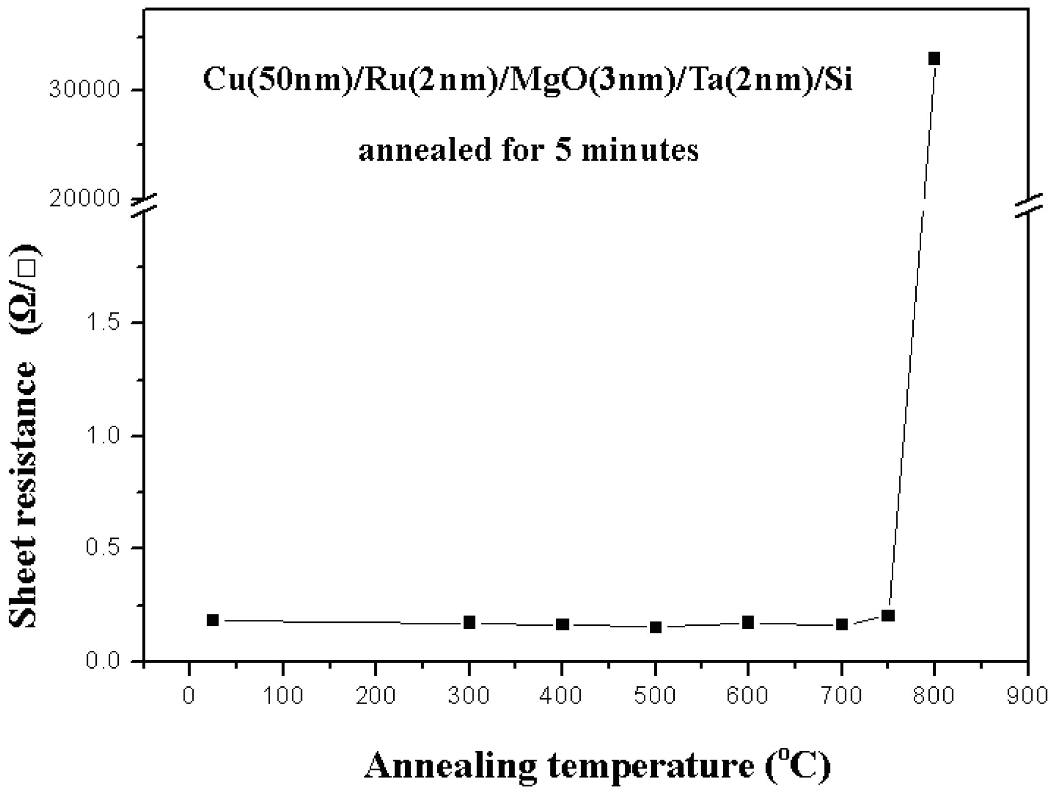
Figure 1 shows the relation between sheet resistance and annealing temperature for a Cu (50 nm)/Ru (2 nm)/MgO (3 nm)/Ta (2 nm)/Si structure annealed for 5 min. The sheet resistances are about 0.25 ohm/square (Ω/ϒ) when the annealing temperature is not higher than 750 °C. However when the annealing temperature is 800 °C, the sheet resistance increases abruptly up to 30,000 ohm/square (Ω/ϒ).
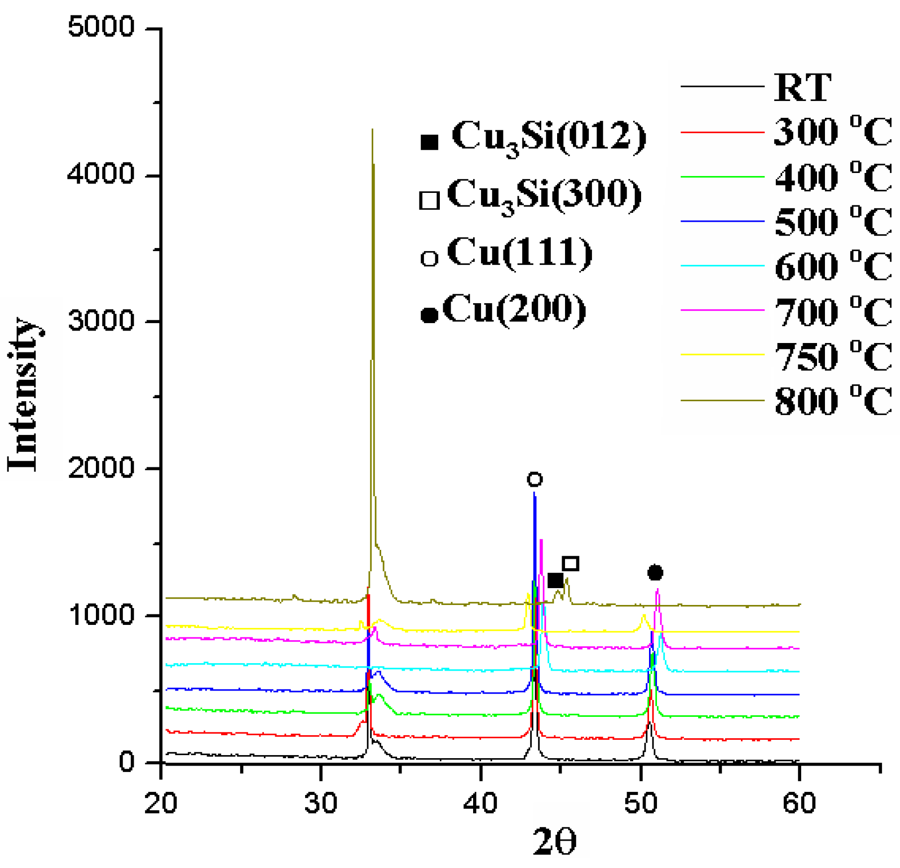
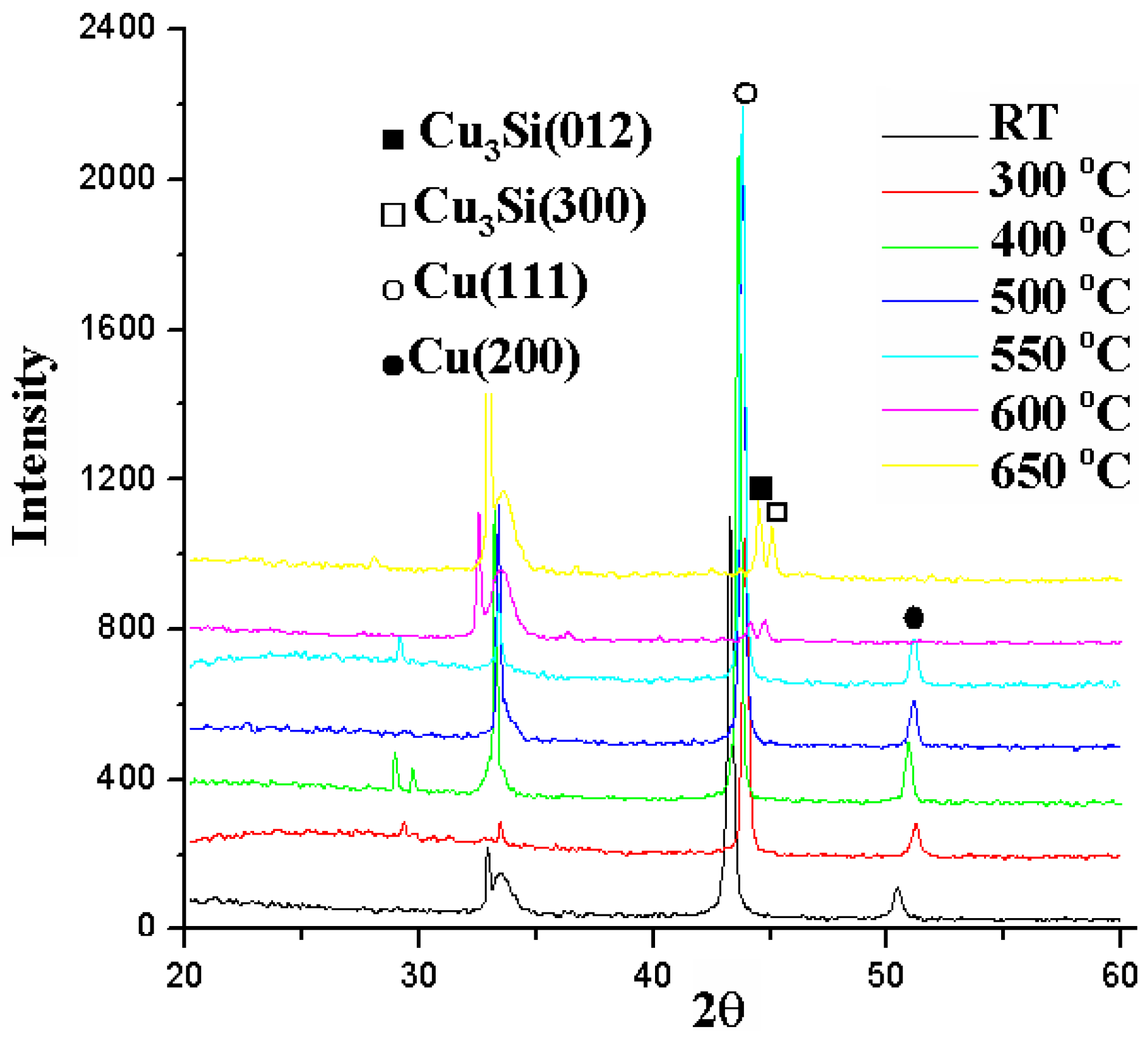
Figure 2 shows the X-ray diffraction patterns for the Cu (50 nm)/Ru (2 nm)/MgO (3 nm)/Ta (2 nm)/Si structure annealed for 5 min at temperatures from 300 to 800 °C. The occurrence of Cu
3Si phase in the structure can explain why the sheet resistance of the structure annealed at 800 °C for 5 min increases abruptly up to that more than 30,000 ohm/square (Ω/ϒ). XRD analysis of the samples after annealing to 750 °C shows almost exactly the same pattern as that of the as-deposited sample except for some changes in relative intensities. Based on these XRD spectra, only copper is present up to 750 °C. At 800 °C, the formation of copper silicide, Cu
3Si, take place according to the XRD. As mention above, the Cu
3Si formation is not observed at the annealing temperature of 750 °C. It is well know that the Cu
3Si phase has been formed by solid-state reaction at a temperature of 200 °C, which is much lower than the annealing temperature used in this study. Thus, Ru (2 nm)/MgO (3 nm)/Ta (2 nm), as a barrier material, is useful to block the diffusion of Cu into Si.
Figure 1.
Relation between sheet resistances and annealing temperatures for Cu (50 nm)/Ru (2 nm)/MgO (3 nm)/Ta (2 nm)/Si structure annealed for 5 min.
Figure 1.
Relation between sheet resistances and annealing temperatures for Cu (50 nm)/Ru (2 nm)/MgO (3 nm)/Ta (2 nm)/Si structure annealed for 5 min.
Figure 2.
X-ray diffraction patterns for the MgO (3 nm) sample annealed for 5 min at temperatures from room temperature to 800 °C.
Figure 2.
X-ray diffraction patterns for the MgO (3 nm) sample annealed for 5 min at temperatures from room temperature to 800 °C.
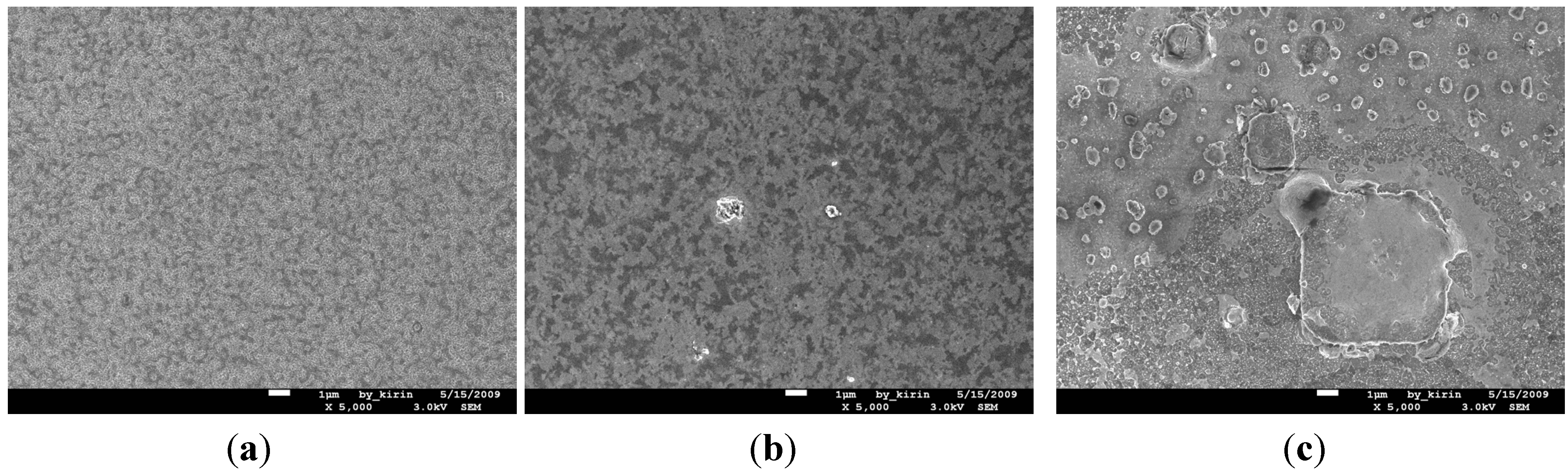
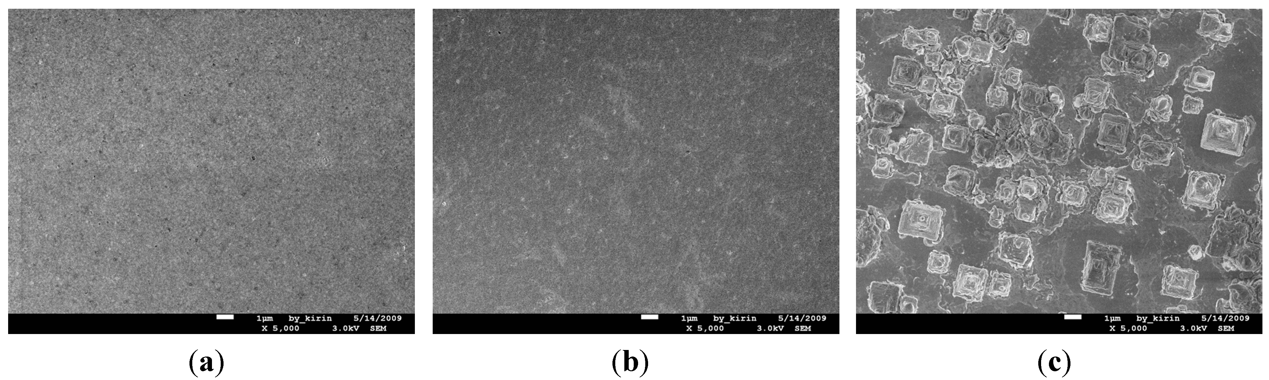
Figure 3a–c show the SEM images for the surface morphologies of Cu (50 nm)/Ru (2 nm)/MgO (3 nm)/Ta (2 nm)/Si structure annealed for 5 min at 700, 750, and 800 °C, respectively. The surface of the structure annealed at 700 °C looks relatively smooth, as shown in
Figure 3a. When annealed at 750 °C, the surface of the structure looks relatively rough, as shown in
Figure 3b, which may be ascribed to the agglomeration of the Cu layer. In
Figure 3c there are many particles with a size of about 0.1–10 nm present at the surface, which are Cu
3Si phase confirmed by the X-ray diffraction, as shown in
Figure 2.
Figure 3.
Scanning electron microscope (SEM) views for the surface morphologies of MgO (3 nm) sample annealed for 5 min at temperatures of 700 °C (a); 750 °C (b); and 800 °C (c); respectively.
Figure 3.
Scanning electron microscope (SEM) views for the surface morphologies of MgO (3 nm) sample annealed for 5 min at temperatures of 700 °C (a); 750 °C (b); and 800 °C (c); respectively.
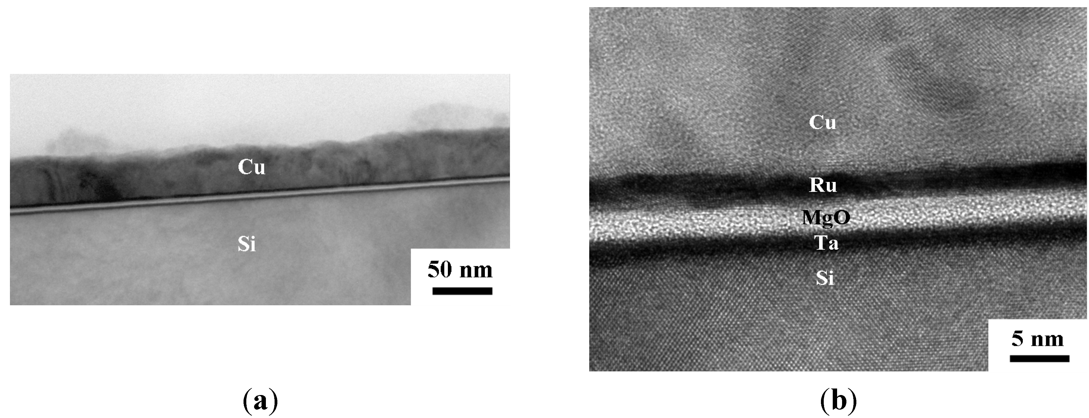
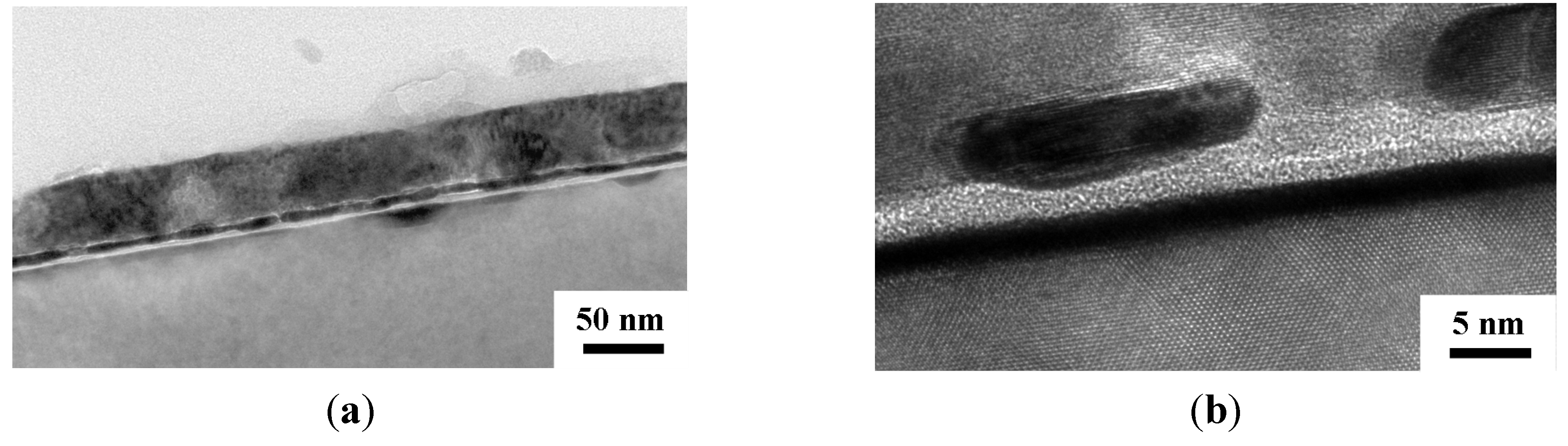
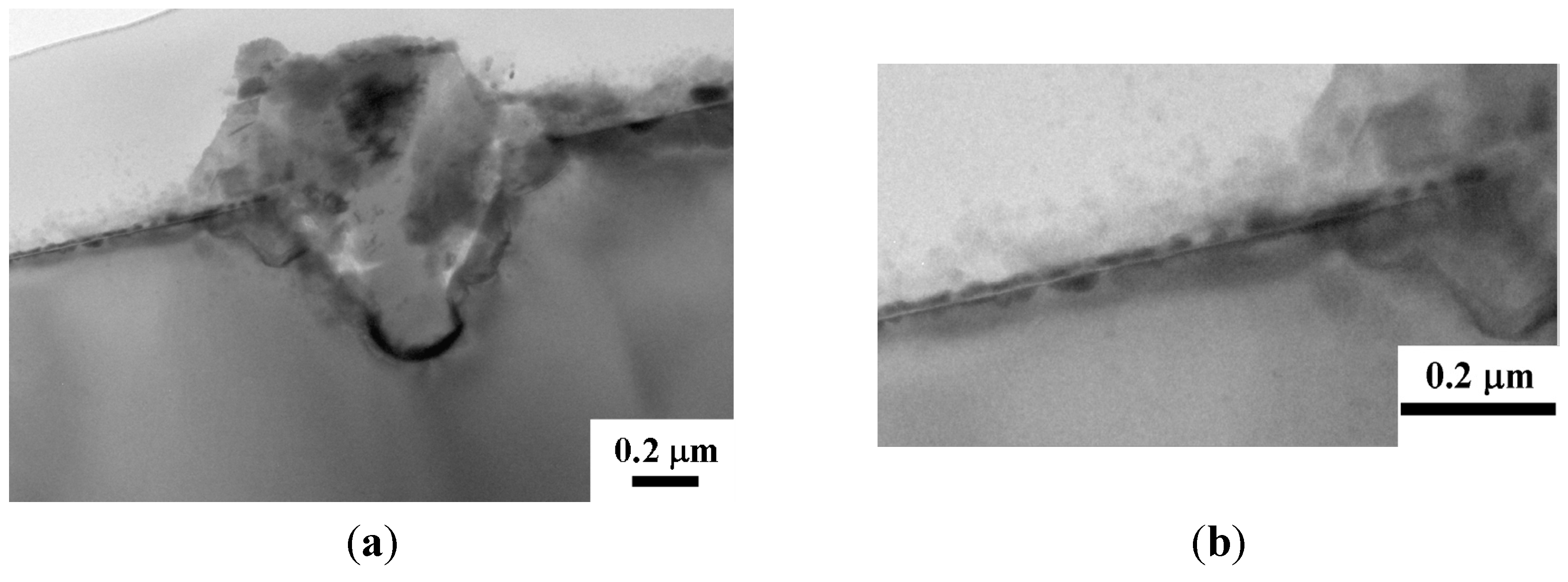
The TEM cross section views for the Cu (50 nm)/Ru (2 nm)/MgO (3 nm)/Ta (2 nm)/Si structure annealed for 5 min at room temperature, 500, 750, and 800 °C are shown in
Figure 4,
Figure 5,
Figure 6 and
Figure 7, respectively. The as-deposited Ru layer, MgO layer, and Ta layer in the structure are quite flat and the MgO layer and Ta layers are amorphous, as shown in
Figure 4a,b. After annealing at 500 °C for 5 min, the surface of the Ru layer, MgO layer, and Ta layer are still flat and the MgO layer and Ta layer are still amorphous, as shown in
Figure 5b. After annealing at 750 °C for 5 min, the MgO layer and Ta layer are still amorphous and continuous, but the Ru layer became discontinuous and there is some Cu diffusion at the discontinuities, as shown in
Figure 6.
Figure 7a shows glom Cu
3Si particle that formed in the structure after annealing for 5 min at 800 °C. An enlarged view of the left part of
Figure 7a is shown in
Figure 7b, which clearly shows that both Ru and Ta layers are discontinous, but the MgO layer seems to be still continuous. Therefore, it can be speculated that the Ru layer first became discontinuous at 750 °C, the Ta layer sequentially became discontinuous at 800 °C, the Cu atoms then can diffuse through the MgO layer and to the substrate at the discontinuities, and the Cu
3Si phase finally form.
Figure 4.
Transmission electron microscope (TEM) cross section views for the MgO (3 nm) sample as deposited at a relatively low magnification (a); and at a relatively high magnification (500,000×) (b).
Figure 4.
Transmission electron microscope (TEM) cross section views for the MgO (3 nm) sample as deposited at a relatively low magnification (a); and at a relatively high magnification (500,000×) (b).
Figure 5.
TEM cross section views for the structures of MgO (3 nm) sample annealed for 5 min at 500 °C at a relatively low magnification (a); and at a relatively high magnification (b).
Figure 5.
TEM cross section views for the structures of MgO (3 nm) sample annealed for 5 min at 500 °C at a relatively low magnification (a); and at a relatively high magnification (b).
Figure 6.
TEM cross section views for the structures of Cu (50 nm)/Ru (2 nm)/MgO (3 nm)/Ta (2 nm)/Si annealed for 5 min at 750 °C at a relatively low magnification (a); and at a relatively high magnification (b).
Figure 6.
TEM cross section views for the structures of Cu (50 nm)/Ru (2 nm)/MgO (3 nm)/Ta (2 nm)/Si annealed for 5 min at 750 °C at a relatively low magnification (a); and at a relatively high magnification (b).
Figure 7.
(a) TEM cross section views for the MgO (3 nm) sample annealed for 5 min at 800 °C; (b) Enlarged view of the left part of (a).
Figure 7.
(a) TEM cross section views for the MgO (3 nm) sample annealed for 5 min at 800 °C; (b) Enlarged view of the left part of (a).
2.2. Cu (50 nm)/Ru (2 nm)/MgO (2 nm)/Ta (2 nm)/Si
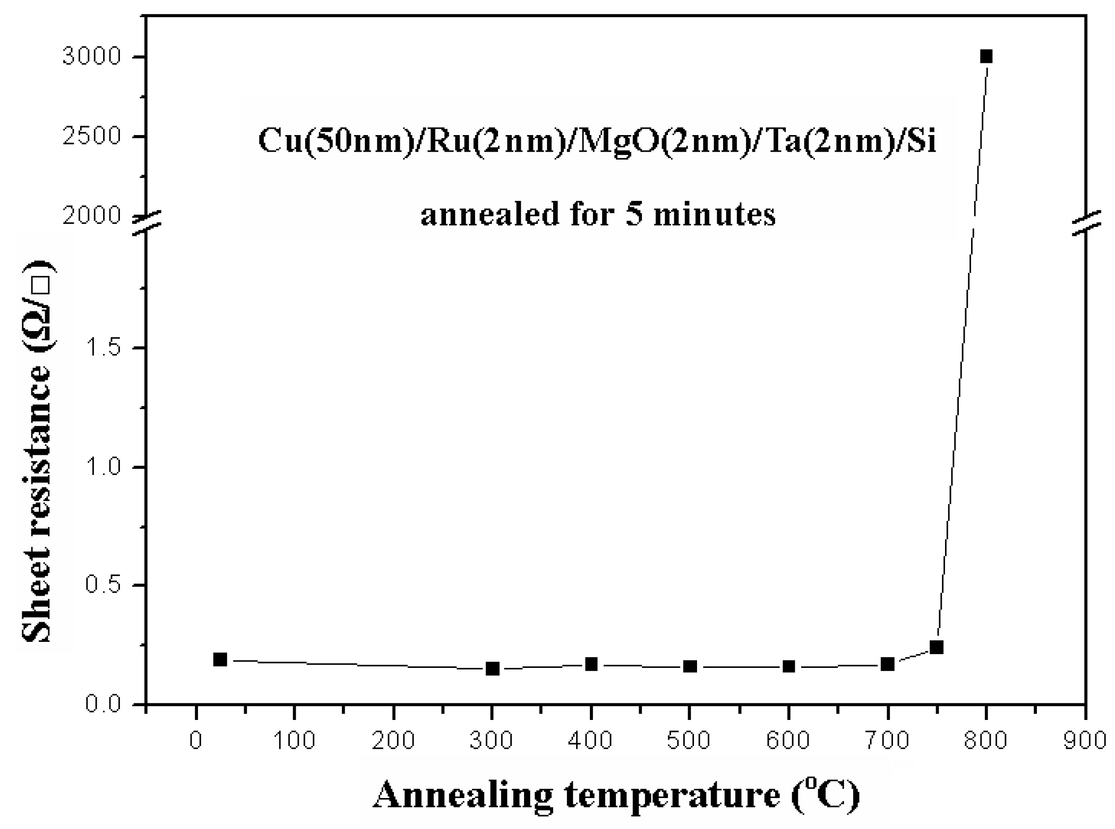
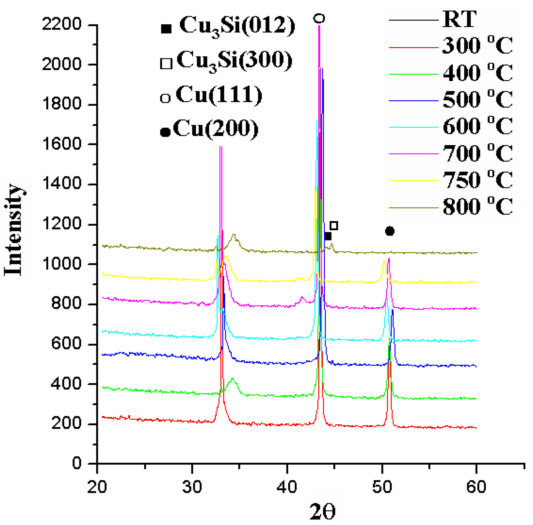
Figure 8 shows the relation between sheet resistances and annealing temperatures for a Cu (50 nm)/Ru (2 nm)/MgO (2 nm)/Ta (2 nm)/Si structure annealed for 5 min. The sheet resistances remain at about 0.25 Ω/ϒ when annealing temperature is not higher than 750 °C, but the sheet resistance increases abruptly up to 3000 Ω/ϒ at 800 °C. The X-ray diffraction patterns for the structure of Cu (50 nm)/Ru (2 nm)/MgO (2 nm)/Ta (2 nm)/Si annealed for 5 min at temperatures from 300 to 800 °C are shown in
Figure 9. The Cu
3Si phase occurs only at annealing temperature of 800 °C.
Figure 8.
Relation between sheet resistances and annealing temperatures for a Cu (50 nm)/Ru (2 nm)/MgO (2 nm)/Ta (2 nm)/Si structure annealed for 5 min.
Figure 8.
Relation between sheet resistances and annealing temperatures for a Cu (50 nm)/Ru (2 nm)/MgO (2 nm)/Ta (2 nm)/Si structure annealed for 5 min.
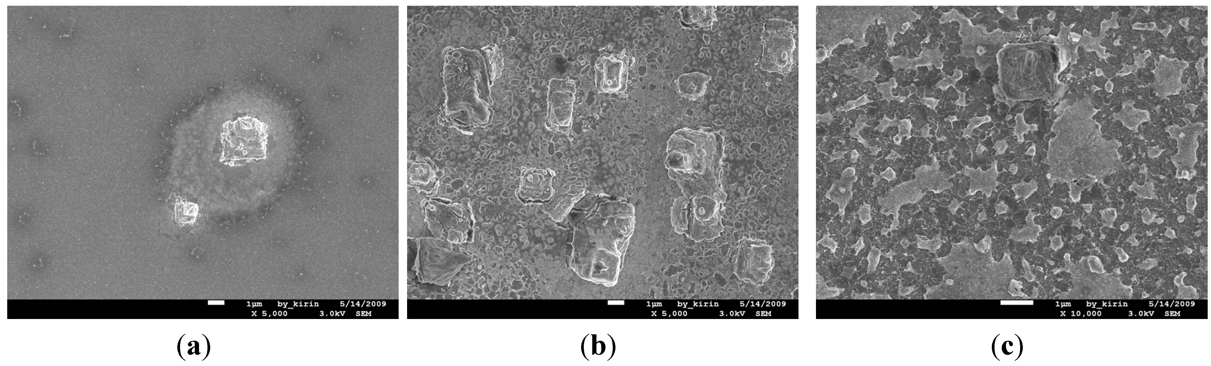
The SEM images for the surface morphologies of Cu (50 nm)/Ru (2 nm)/MgO (2 nm)/Ta (2 nm)/Si structures annealed for 5 min at 700, 750, and 800 °C are shown in
Figure 10a–c, respectively. The surface of the structure annealed at 700 °C looks smooth. There are several 1 μm particles on the surface of the structure after annealing at 750 °C.
Figure 10c shows there are many particles about 0.1–10 μm on the surface of the structure annealing at 800 °C.
Although the peaks of Cu
3Si phase occur only at the X-ray diffraction pattern for the structure annealed at 800 °C, as shown in
Figure 9, the Cu
3Si particles have emerged on the surface of the structure annealed at 750 °C, as shown in
Figure 10b and the sheet resistance of this structure is slightly larger than the structure annealed at 700 °C. The reason for the inconsistent phenomena may be ascribed that the amount of the Cu
3Si phase is too small to be detected by the X-ray diffraction method.
Figure 9.
X-ray diffraction patterns for the structures of MgO (2 nm) sample annealed for 5 min at temperatures from room temperature to 800 °C.
Figure 9.
X-ray diffraction patterns for the structures of MgO (2 nm) sample annealed for 5 min at temperatures from room temperature to 800 °C.
Figure 10.
SEM views for the surface morphologies of structures of MgO (2 nm) sample annealed for 5 min at temperatures 700 °C (a); 750 °C (b); and 800 °C (c); respectively.
Figure 10.
SEM views for the surface morphologies of structures of MgO (2 nm) sample annealed for 5 min at temperatures 700 °C (a); 750 °C (b); and 800 °C (c); respectively.
2.3. Cu (50 nm)/Ru (2 nm)/MgO (1 nm)/Ta (2 nm)/Si
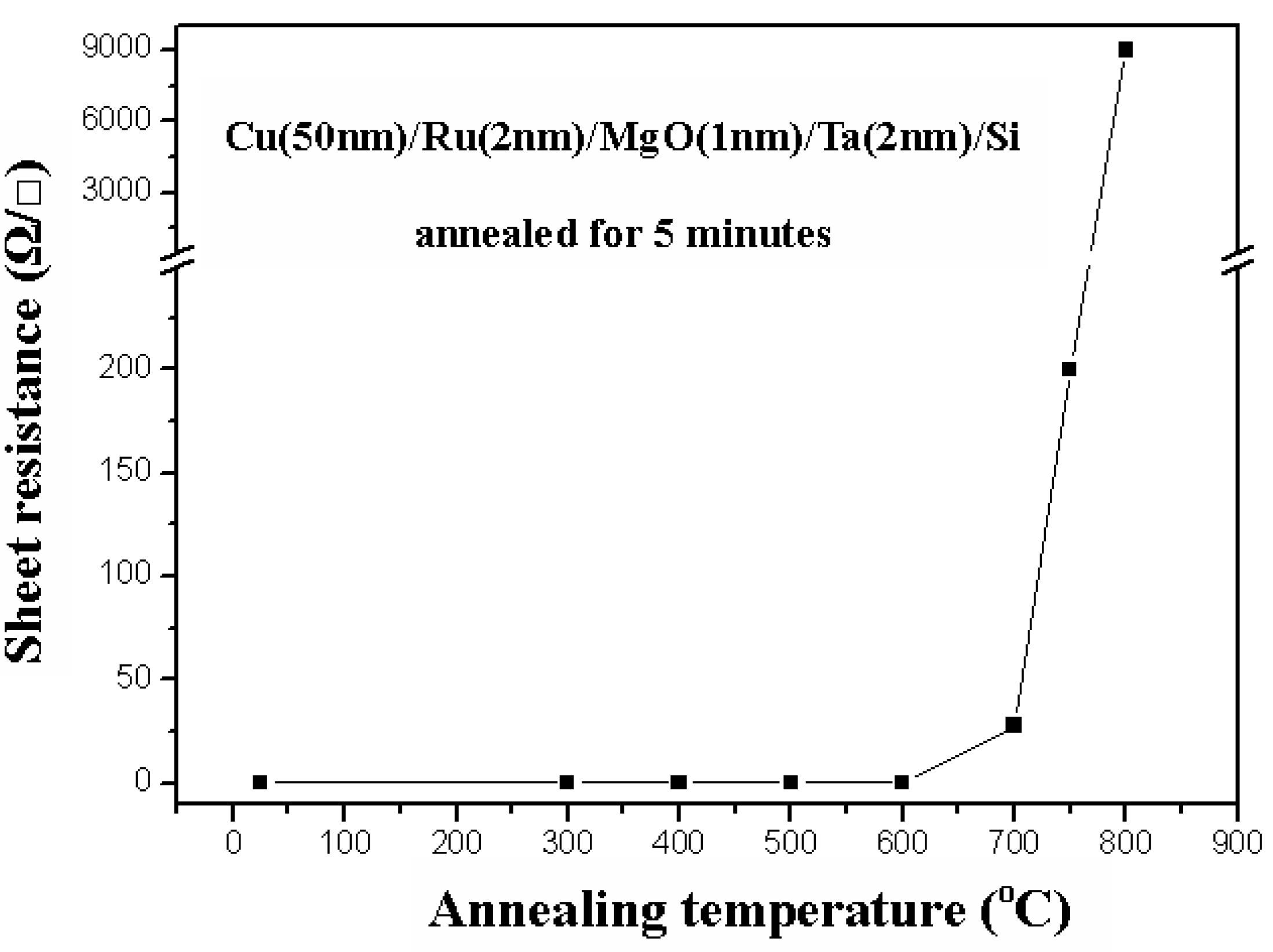
The relation between sheet resistance and annealing temperature for the Cu (50 nm)/Ru (2 nm)/MgO (1 nm)/Ta (2 nm)/Si structures annealed for 5 min is shown in
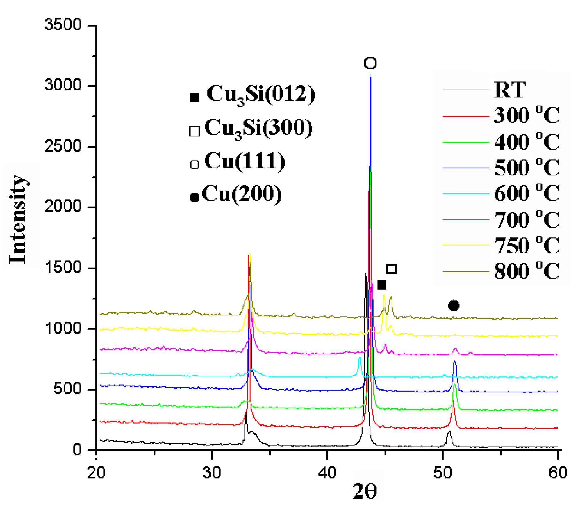
Figure 11, in which the sheet resistances are about 0.25 Ω/ϒ for the structures annealed at a temperature lower than 600 °C, about 35 Ω/ϒ for 700 °C, about 200 Ω/ϒ for 750 °C, and increases abruptly up to 9000 Ω/ϒ for 800 °C. The X-ray diffraction patterns for the Cu (50 nm)/Ru (2 nm)/MgO (1 nm)/Ta (2 nm)/Si structures annealed for 5 min at room temperature to 800 °C are shown in
Figure 12, in which the Cu
3Si phase peaks appear at annealing temperature of 700, 750, and 800 °C.
Figure 11.
Relation between sheet resistance and annealing temperature for Cu (50 nm)/Ru (2 nm)/MgO (1 nm)/Ta (2 nm)/Si structures annealed for 5 min.
Figure 11.
Relation between sheet resistance and annealing temperature for Cu (50 nm)/Ru (2 nm)/MgO (1 nm)/Ta (2 nm)/Si structures annealed for 5 min.
Figure 12.
X-ray diffraction patterns for the structures of MgO (1 nm) sample annealed for 5 min at temperatures from room temperature to 800 °C.
Figure 12.
X-ray diffraction patterns for the structures of MgO (1 nm) sample annealed for 5 min at temperatures from room temperature to 800 °C.
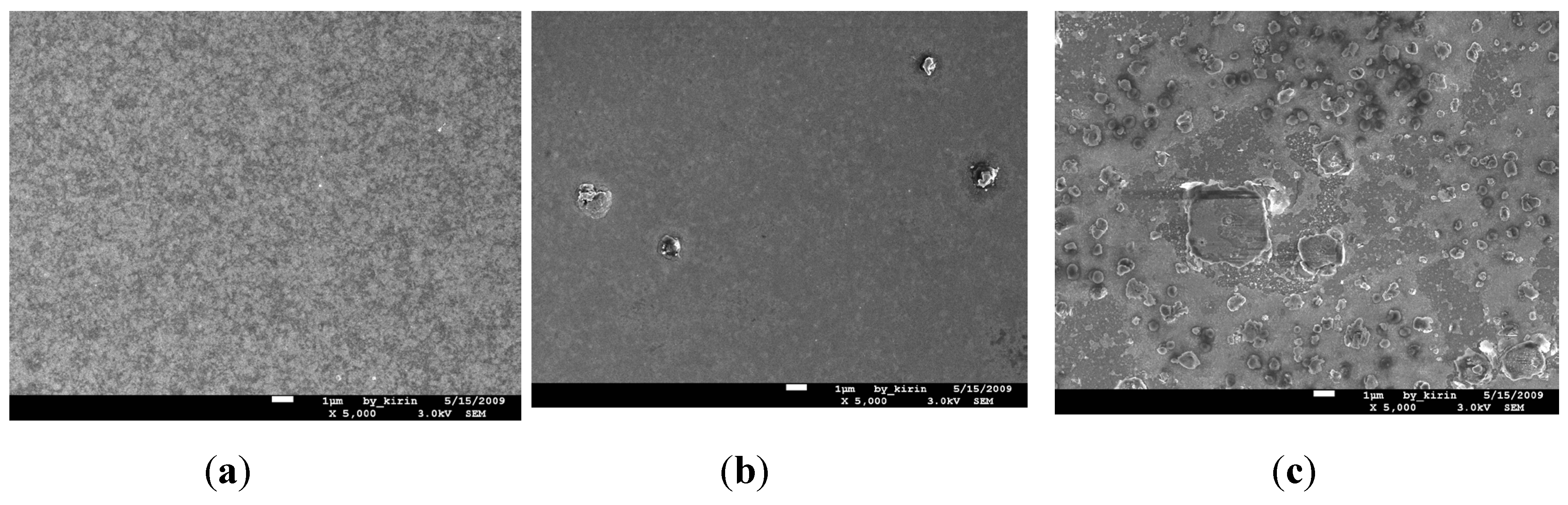
The SEM images for the surface morphologies of the Cu (50 nm)/Ru (2 nm)/MgO (1 nm)/Ta (2 nm)/Si structures annealed for 5 min at 700 °C, 750, and 800 °C are shown in
Figure 13a–c, respectively. The number of Cu
3Si particles emerged on the surface increases with the increase of annealing temperature from 700 °C to 800 °C. It is obvious that there is a consistence among the sheet resistance, Cu
3Si phase, and surface morphology for the structures annealed for 5 min at room temperature to 800 °C.
Figure 13.
SEM views for the surface morphologies of structures of MgO (1 nm) sample annealed for 5 min at temperatures at 700 °C (a); 750 °C (b); and 800 °C (c); respectively.
Figure 13.
SEM views for the surface morphologies of structures of MgO (1 nm) sample annealed for 5 min at temperatures at 700 °C (a); 750 °C (b); and 800 °C (c); respectively.
2.4. Cu (50 nm)/Ru (2 nm)/MgO (0.5 nm)/Ta (2 nm)/Si
Figure 14 shows the relation between sheet resistance and annealing temperature for the Cu (50 nm)/Ru (2 nm)/MgO (0.5 nm)/Ta (2 nm)/Si structures annealed for 5 min. When the annealing temperature is equal to and lower than 550 °C, the sheet resistances are about 0.25 Ω/ϒ, and when the annealing temperature is 600 °C, the sheet resistance increases to about 150 Ω/ϒ.
Figure 15 shows the X-ray diffraction patterns for the structures of Cu (50 nm)/Ru (2 nm)/MgO (0.5 nm)/Ta (2 nm)/Si annealed for 5 min at a temperature from room temperature to 650 °C. It can be seen that the Cu
3Si phase peaks emerge at 600 °C and 650 °C.
Figure 16a–c show the SEM images for the surface morphologies of the Cu (50 nm)/Ru (2 nm)/MgO (0.5 nm)/Ta (2 nm)/Si structures annealed for 5 min at a temperature of 500, 550, and 600 °C, respectively. The surface is quite smooth in
Figure 16a annealed at 500 °C, more or less rough in
Figure 16b annealed at 550 °C, and has many Cu
3Si particles in
Figure 16c annealed at 600 °C. It can be seen from
Figure 14,
Figure 15 and
Figure 16 that there is also a correspondence between the sheet resistance, Cu
3Si phase, and surface morphology for the structures annealed for 5 min at room temperature to 600 °C.
Figure 14.
Relation between sheet resistances and annealing temperatures for the Cu (50 nm)/Ru (2 nm)/MgO (0.5 nm)/Ta (2 nm)/Si structures annealed for 5 min.
Figure 14.
Relation between sheet resistances and annealing temperatures for the Cu (50 nm)/Ru (2 nm)/MgO (0.5 nm)/Ta (2 nm)/Si structures annealed for 5 min.
Figure 15.
X-ray diffraction patterns for the structures of MgO (0.5 nm) sample annealed for 5 min at temperatures from room temperature to 650 °C.
Figure 15.
X-ray diffraction patterns for the structures of MgO (0.5 nm) sample annealed for 5 min at temperatures from room temperature to 650 °C.
Figure 16.
SEM images for the surface morphologies of structures of MgO (0.5 nm) sample annealed for 5 min at temperature 500 °C (a); 550 °C (b); and 600 °C (c), respectively.
Figure 16.
SEM images for the surface morphologies of structures of MgO (0.5 nm) sample annealed for 5 min at temperature 500 °C (a); 550 °C (b); and 600 °C (c), respectively.


