Abstract
In this paper, we propose a simple and efficient method for designing a broadband terahertz (THz) absorber based on singular graphene patches metasurface and metal-backed dielectric layer. An accurate circuit model of graphene patches is used for obtaining analytical expressions for the input impedance of the proposed absorber. The input impedance is designed to be closely matched to the free space in a wide frequency range. Numerical simulation and analytical circuit model results consistently show that graphene metasurface-based THz absorber with an absorption value above 90% in a relative bandwidth of 100% has been achieved.
1. Introduction
Terahertz (0.1–10 THz) absorbers have attracted great interest for their extensive applications in sensing [1], imaging [2], detecting [3], modulation [4], thermal emitters [5], and so on. However, THz electromagnetic waves are very hard to be detected by natural materials [6]. Metamaterial absorbers (MAs), a new type of artificially structured electromagnetic materials, have drawn much attention in recent years due to its extraordinary electronic and optical properties [7,8,9,10,11]. This is especially important for a broad THz frequency range that can realize near-unity absorption [12,13].
Graphene, a material consisting of one monolayer of carbon atoms, has been widely investigated as a promising platform for designing broadband tunable MAs in THz regime due to its exotic properties, such as optical transparency, high absorption, high electron mobility [14,15]. In addition, its sheet conductivity depending on chemical potential can be continuously tuned in a broad frequency range by tuning the gate voltage or chemical doping [16,17]. Recently, several broadband graphene-based MAs have been proposed [18,19,20,21,22,23,24]. However, most of these works only show specific structures having broadband absorption and few investigations explain the way to design the structure in order to get the desired broadband absorption in the graphene-based MAs.
In this paper, a simple and efficient method for designing broadband THz MAs based on a periodical monolayered graphene patch array has been proposed. This method is based on the equivalent circuit model, in which an analytical surface admittance is employed to describe the properties of the graphene metasurface. Moreover, Conditions for broadband absorption have been analyzed. A set of closed-form relations for material properties and geometrical parameters of the absorber have been derived. As a consequence, we can successfully design a broadband THz absorber for a given central frequency based on the formulas derived from this approach. To validate the approach, the results have been compared with those obtained by the finite-difference time-domain (FDTD Solutions, Lumerical Inc., Vancouver, BC, Canada) simulations, excellent agreements have been achieved.
2. Equivalent Circuit Model Approach
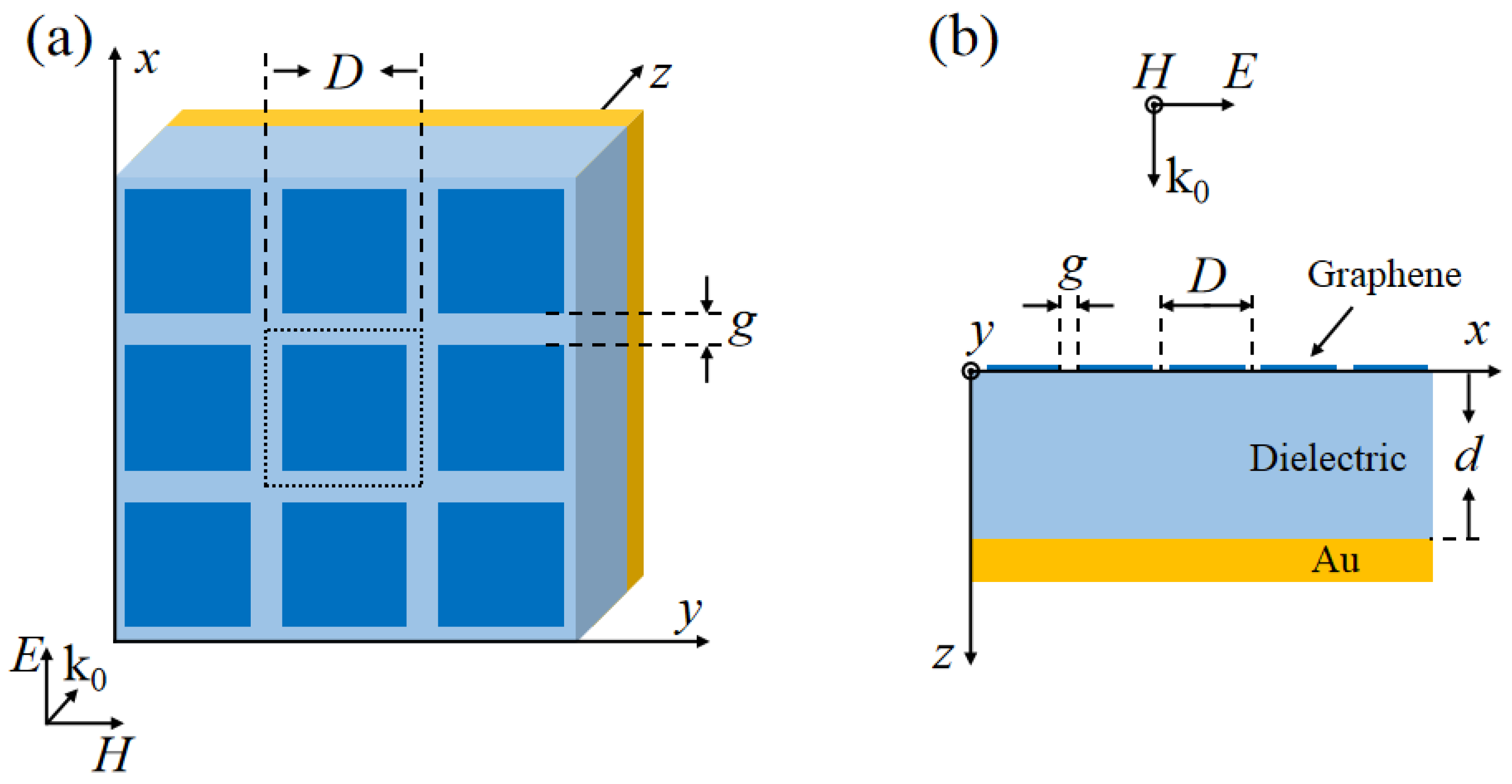
To realize electromagnetic wave absorbers at THz frequency, we can take a simple structure. A schematic of the proposed absorber is shown in Figure 1. The structure consists of a sheet of periodic graphene patches on the top, a dielectric spacer layer, and a ground plate on the bottom. The graphene patches are periodically arranged along the x and y directions and embedded into the dielectric material. This layer is used to induce high absorption. The dielectric spacer layer has a refractive index of and low losses in THz band. The bottom layer is made of gold with a conductivity of S/m and a thickness of 0.5 m. As the thickness of the gold used here is much lager than the typical skin depth in the THz regime, the gold layer is acting as a reflector.
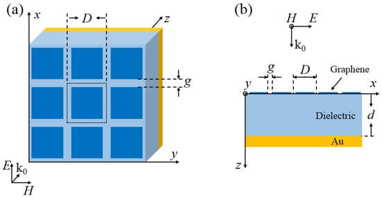
Figure 1.
Schematic diagram of the proposed absorber: (a) perspective view. (b) side view.
As we know, the surface conductivity of graphene is composed of interband and intraband contributions derived using the Kubo formula [25]. In the THz regime, where the photon energy ( is the chemical potential), the interband contribution of the surface conductivity can be neglected. Thus, the surface conductivity of the graphene has a Drude form [26,27]:
where
where e is the electron charge, is Boltzmann’s constant, ℏ is the reduced Planck’s constant, is the carrier relaxation time, T is the temperature, is the angular frequency. In this paper, we use K and s [28].
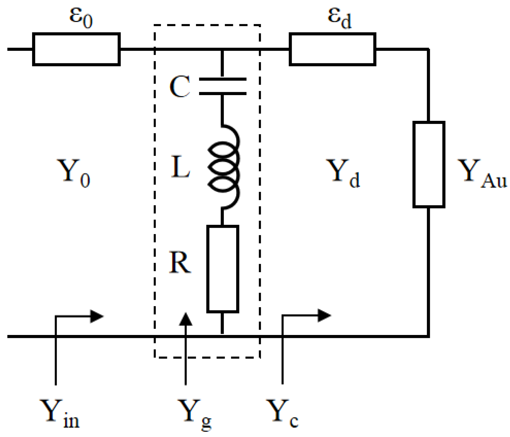
Here, we use an equivalent circuit model to design the broadband graphene-based absorber. Based on the transmission line theory, the whole structure of the absorber can be considered as circuit elements [28]. The equivalent circuit of the device at normal incidence for TM polarization (electric field along the x direction) is illustrated in Figure 2. In this circuit model, the top graphene patch array can be modeled with a shunt admittance . The homogeneous regions, namely, the free space and the dielectric spacer are modeled as transmission lines. The bottom metal can be represented by the admittance .
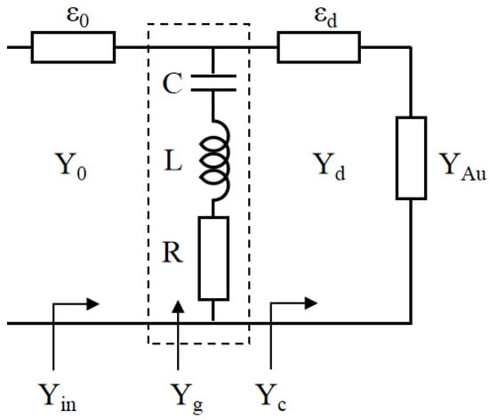
Figure 2.
Equivalent circuit model for the graphene metasurface-based absorber.
Models for the graphene patch array have been presented in several studies [29,30,31]. Barzegar-Parizi et al. proposed an accurate analytical R-L-C circuit model [29]. The results calculated by the circuit model agreed well with those by full-wave simulations, demonstrating that the circuit model is accurate and effective. However, the value of C in the formula has to be carried out numerically. Meanwhile, a simple closed-form expression for graphene patch array was introduced by Padooru et al. in Reference [30]. The model showed considerable discrepancies with the full-wave simulations, which was demonstrated in Reference [29]. Moreover, the capacitive impedance of metal square patches has been modeled by Luukkonen et al. in Reference [31]. Results by the models were verified with good accuracy compared with those by full-wave simulations. Combining the models proposed in References [29,31], here we propose a simple and accurate analytical circuit model for graphene patches. The surface admittance of the graphene patch array can be written as:
where a is the weighted coefficient, D is the period of the patch array, g is the gap between the graphene patches (), is the average permittivity of the mediums surrounding the graphene patches, is the dielectric constant of vacuum and is the relative permittivity of the dielectric material. It can be seen that the graphene patch array can be modeled by a series R-L-C circuit, where R and L are produced by the graphene patches, corresponded to the surface impedance and the geometric factor . we get by analyzing the fundamental resonant mode of the array. it should be noted that neglecting the effect of higher order modes of the patch array for simplicity of calculation does not affect the accuracy of the model [29]. The C is induced by the gaps between the patches, associated with the patch geometry and background environment [31].
The ground plate of Au can be represented by a short circuit which is suppressing the transmittance, that is . So the input admittance of the metal-backed dielectric layer can be expressed as:
where and are the admittance and the propagation of the transmission line corresponding to the dielectric spacer layer, respectively. , where is the admittance of free space, d is the thickness of the dielectric, c is the speed of light in free space.
With the aid of the above analysis, the total input impedance of the absorber is
The reflection coefficient from the top interface of absorber and free space is assessed as follows:
So the power absorbance A of the absorber is
3. Broadband Absorber Design
We now design an THz absorber to achieve it broadband absorption. Firstly, we’d like to analyze the situation of achieving perfect absorption. It is well known that the conditions for perfect absorption are and . It can be realized for a given central frequency, , by setting , and . So the conditions for perfect absorption can be summarized as follow:
Let us design a perfect absorber for a central frequency at 1 THz. The geometrical parameters of the designed graphene metasurface is assumed to be , the period and gap of the graphene patches are given by Equations (11) and (12) as m and m, the chemical potential of the graphene patch array can be calculated from Equation (11) as eV. Finally, from Equation (13), we obtain the thickness of the dielectric spacer m.
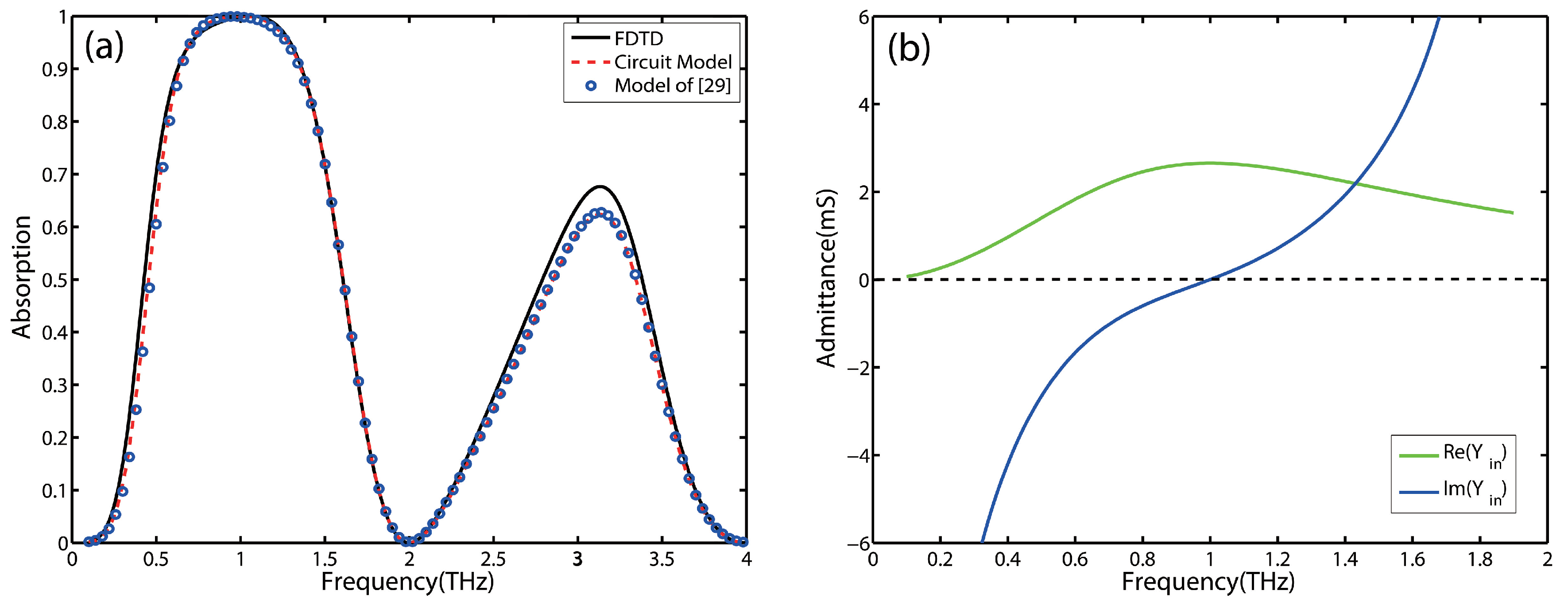
With the aid of the above analytical equations, a perfect absorber for a given central frequency is designed. Figure 3a shows the absorption of this structure calculated by the equivalent circuit model (dotted line) and FDTD simulations (solid line). An excellent agreement can be observed between the two results, which demonstrates that the equivalent circuit model can accurately reflect the absorber’s performance. It should be pointed out that there are slight disagreements around the second absorption peak due to the ignorance of higher order modes in the equivalent circuit model. Moreover, we compare the results obtained by the proposed circuit model with those obtained by the model of Reference [29]. The circles in Figure 3a show the results produced by the model of Reference [29]. The absorptions predicted by the two circuit models are almost coincide. This shows that it is effective to use a simple closed-form expression of C reported in Reference [31] instead of that proposed in [29].
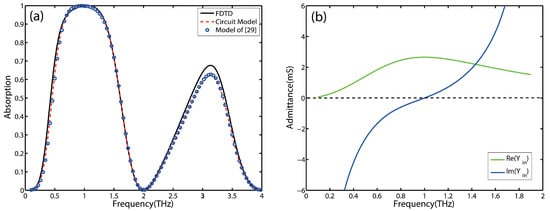
Figure 3.
(a) The absorption spectrum of the designed perfect absorber with the central frequency at 1 THz simulated by FDTD simulations and calculated by circuit model. (b) Real and imaginary parts of the input admittance of the designed absorber.
It can be seen that the absorption decreases rapidly with the corresponding frequency away from the perfect matching point in Figure 3a. Moreover, the bandwith of absorption is just about 0.73 THz. So the conditions for perfect absorption do not lead to broadband absorption. Furthermore, the real and imaginary parts of the input admittance of the designed absorber are depicted in Figure 3b. It can be seen that the sharp absorption spectrum of the perfect absorber is mainly caused by a steep change from 0 to large in the imaginary part of the equivalent circuit, whereas the changes around the central frequency in the real part are relatively flat.
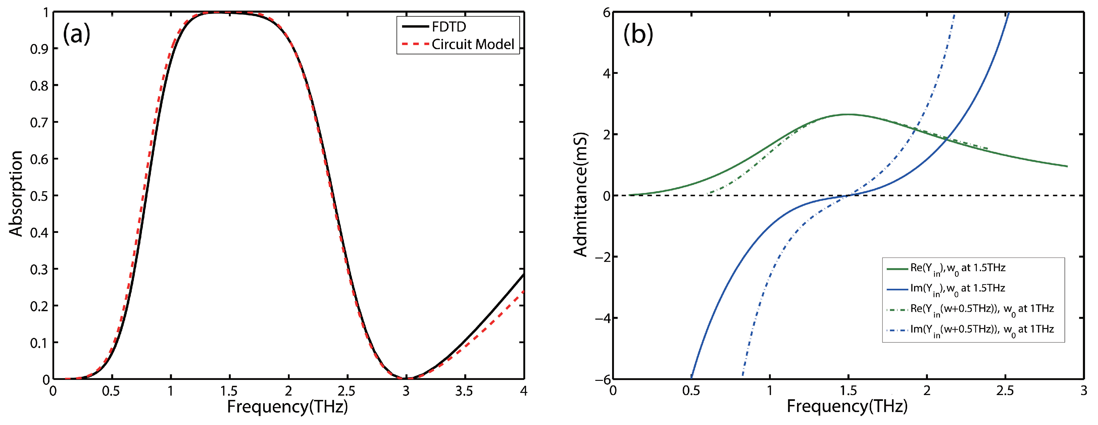
To further verify the inpact of real and imaginary part of the input admittance upon the absorption of the absorber, We test the absorption spectra of a perfect absorber with the central frequency at 1.5 THz (Figure 4a). The bandwidth of absorption reaches about 0.99 THz, which is much wider than the bandwidth at the central frequency of 1 THz (0.73 THz in Figure 3a). The real and imaginary part are also plotted in Figure 4b, which allows us to compare the trends around the central frequency of the two parts. A relatively gentle change in the imaginary part of the absorber with the central frequency of 1.5 THz is corresponding to a wider high absorption bandwidth around the central frequency. Therefore, in order to obtain broadband absorption, we attach an additional condition on the imaginary part of the input admittance:
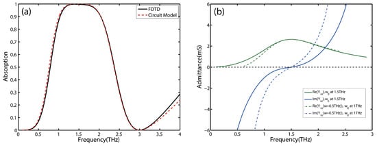
Figure 4.
(a) The absorption spectrum of the designed perfect absorber with the central frequency at 1.5 THz simulated by FDTD simulations and calculated by circuit model. (b) The trends of real and imaginary of the input admittance of the designed absorber with the central frequency at 1.5 THz vs. that of the prefect absorber with the central frequency at 1 THz.
The additional condition leads to a small and slowly varying imaginary part in a wide range of frequencies near the central frequency [32]. With , the input admittance of the metal-backed dielectric layer around can be expressed by Taylor formula:
Similarly, the admittance of the graphene metasurface for frequencies around can be expressed as:
Differentiating Equations (15) and (16) at , the resistance of the graphene array, R, is then obtained from Equation (14):
Moreover, in order to fulfill the requirement of a broadband absorption (), there is a limitation on the central frequency:
which results in
In conclusion. The conditions for broadband absorption can be summarised as Equations (12), (13), (17), and (19). Now let us design a broadband absorber. According to Equations (17) and (19), when the material has a dielectric constant at , high absorption can be achieved at the central frequency of 1 THz. In the constraint condition (Equation (17)), we set the geometrical parameters of designed graphene metasurface at and get a chemical potential of the graphene patches at eV. The period and gap of patches can be easily calculated by Equation (12), one obtains m and m. Moreover, the thickness of the dielectric spacer is obtained from Equation (13) as m.
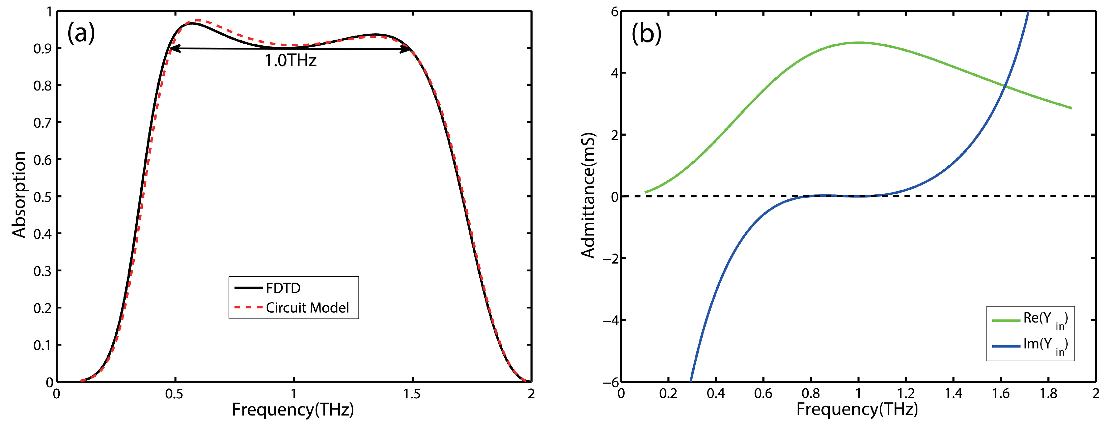
The absorption of this structure is shown in Figure 5a. It can be observed that the effective absorption bandwidth (above ) is from 0.47 to 1.47 THz, indicating a relative absorption bandwidth of . As it is shown that the real and imaginary parts of the input admittance, , in Figure 5b. The imaginary part of the input admittance is near zero and changes slowly around the central frequency, while the real part of the input admittance remains a small reduction near in the corresponding frequency range. These features lead to wide-band impedance matching. Thus, a broadband absorption can be realized.
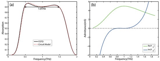
Figure 5.
(a) The absorption spectrum of the designed broadband absorber with the central frequency at 1 THz simulated by FDTD simulations and calculated by circuit model. (b) Real and imaginary parts of the input admittance of the designed absorber.
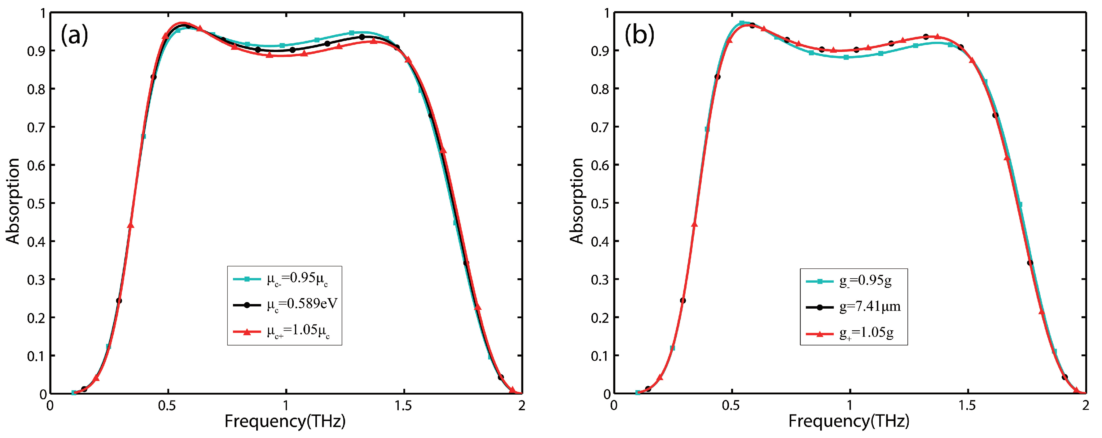
Considering the actual manufacturing errors, effect of the variations of Fermi energy and gap of graphene patches on the absorber performance are examined. As shown in Figure 6a, there are no significant change on high absorption bandwidth for variation in the Fermi energy of graphene patches. Moreover, it can be seen from Figure 6b that the high absorption characteristics of the absorber is not very sensitive for variation in the gap of graphene patches.
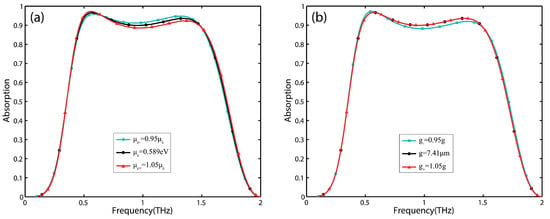
Figure 6.
The absorption spectrum of the absorber calculated by full-wave simulation for: (a) three different Fermi energy of graphene patches. (b) three different gaps of graphene patches.
It should be pointed that the design algorithm has some limitations. Firstly, to achieve high absorption, R should be large than . Since here is a constant, the central frequency cannot be chosen arbitrarily, That is THz. The other limitation deserves attention. The period of patch arrays must be much smaller than the wavelength and must be much smaller than unity. Otherwise, the proposed circuit model would not be valid [33].
4. Conclusions
A novel approach for graphene metasurface-based broadband THz absorber design has been proposed. This approach significantly simplified the design of broadband THz absorbers. Based on the equivalent circuit model, the imaginary part of the absorber input admittance and its derivative are designed to be zero at a given center frequency. Then, the real part of the device input admittance is tuned to match the free-space admittance around the central frequency. As a result, a relative absorption bandwidth of is realized by using only one layer of graphene metasurface. The results also have been compared with FDTD simulations and good agreements have been achieved. It can be concluded that the proposed approach can provide an effective method to analyze and design graphene-based broadband absorbers.
Author Contributions
Formal analysis and writing–original draft preparation, Z.L.; investigation, L.G.; writing–review and editing, Q.Z.
Funding
This research was supported by the National Key Research and Development Program of China (2017YFB1104500), the National Science Foundation of Guangdong Province (2016A030313456), the Science and Technology Planning Project of Guangdong Province (2018B030323017, 2016B090917002).
Acknowledgments
This research was supported by the National Key Research and Development Program of China (2017YFB1104500), the National Science Foundation of Guangdong Province (2016A030313456), the Science and Technology Project of Guangdong Province (2018B030323017, 2016B090917002) and Guangdong Provincial Key Laboratory of Industrial Ultrashort Pulse Laser Technology, Shenzhen 518055, China.
Conflicts of Interest
The authors declare no conflict of interest.
References
- Alves, F.; Grbovic, D.; Kearney, B.; Lavrik, N.V.; Karunasiri, G. Bi-material terahertz sensors using metamaterial structures. Opt. Express 2013, 21, 13256–13270. [Google Scholar] [CrossRef] [PubMed]
- Carranza, I.E.; Grant, J.P.; Gough, J.; Cumming, D. Terahertz metamaterial absorbers implemented in CMOS technology for imaging applications: Scaling to large format focal plane arrays. IEEE J. Sel. Top. Quantum Electron. 2017, 23, 4700508. [Google Scholar]
- Mittendorff, M.; Winnerl, S.; Kamann, J.; Eroms, J.; Weiss, D.; Schneider, H.; Helm, M. Ultrafast graphene-based broadband THz detector. Appl. Phys. Lett. 2013, 103, 021113. [Google Scholar] [CrossRef]
- Le, L.N.; Thang, N.M.; Thuy, L.M.; Tung, N.T. Hybrid semiconductor–dielectric metamaterial modulation for switchable bi-directional THz absorbers. Opt. Commun. 2017, 383, 244–249. [Google Scholar] [CrossRef]
- Wang, B.X.; Wang, L.L.; Wang, G.Z.; Huang, W.Q.; Li, X.F.; Zhai, X. Frequency Continuous Tunable Terahertz Metamaterial Absorber. J. Lightwave Technol. 2014, 32, 1183–1189. [Google Scholar] [CrossRef]
- Williams, G.P. Filling the THz gap-high power sources and applications. Rep. Prog. Phys. 2006, 69, 301–326. [Google Scholar] [CrossRef]
- Landy, N.I.; Sajuyigbe, S.; Mock, J.J.; Smith, D.R.; Padilla, W.J. Perfect Metamaterial Absorber. Phys. Rev. Lett. 2008, 100, 207402. [Google Scholar] [CrossRef]
- Cong, L.; Tan, S.; Yahiaoui, R.; Yan, F.P.; Zhang, W.; Singh, R. Experimental demonstration of ultrasensitive sensing with terahertz metamaterial absorbers: A comparison with the metasurfaces. Appl. Phys. Lett. 2015, 106, 001107. [Google Scholar] [CrossRef]
- Glybovski, S.B.; Tretyakov, S.A.; Belov, P.A.; Kivshar, Y.S.; Simovski, C.R. Metasurfaces: From microwaves to visible. Phys. Rep. 2016, 634, 1–72. [Google Scholar] [CrossRef]
- Liu, X.; Fan, K.; Shadrivov, I.V.; Padilla, W.J. Experimental realization of a terahertz all-dielectric metasurface absorber. Opt. Express 2017, 25, 191–201. [Google Scholar] [CrossRef]
- Yi, Z.; Chen, J.; Cen, C.; Chen, X.; Zhou, Z.; Tang, Y.; Ye, X.; Xiao, S.; Luo, W.; Wu, P. Tunable Graphene-based Plasmonic Perfect Metamaterial Absorber in the THz Region. Micromachines 2019, 10, 194. [Google Scholar] [CrossRef] [PubMed]
- Rahmanzadeh, M.; Rajabalipanah, H.; Abdolali, A. Multilayer graphene-based metasurfaces: Robust design method for extremely broadband, wide-angle, and polarization-insensitive terahertz absorbers. Appl. Opt. 2018, 57, 959–968. [Google Scholar] [CrossRef] [PubMed]
- Yu, P.; Besteiro, L.V.; Huang, Y.; Wu, J.; Fu, L.; Tan, H.H.; Jagadish, C.; Wiederrecht, G.P.; Govorov, A.O.; Wang, Z. Broadband Metamaterial Absorbers. Adv. Opt. Mater. 2019, 7, 1800995. [Google Scholar] [CrossRef]
- Novoselov, K.S.; Fal’ko, V.I.; Colombo, L.; Gellert, P.R.; Schwab, M.G.; Kim, K. A roadmap for graphene. Nature 2012, 490, 192–200. [Google Scholar] [CrossRef] [PubMed]
- Bae, S.; Kim, H.; Lee, Y.; Xu, X.; Park, J.-S.; Zheng, Y.; Balakrishnan, J.; Lei, T.; Kim, H.R.; Song, Y.I.; et al. Roll-to-roll production of 30-inch graphene films for transparent electrodes. Nat. Nanotechnol. 2010, 5, 574–578. [Google Scholar] [CrossRef] [PubMed]
- Xiao, B.; Gu, M.; Qin, K.; Xiao, S. Absorption enhancement in graphene with an efficient resonator. Opt. Quantum Electron. 2017, 49, 1013–1018. [Google Scholar] [CrossRef]
- Zhu, Z.H.; Guo, C.C.; Liu, K.; Zhang, J.F.; Ye, W.M.; Yuan, X.D.; Qin, S.Q. Electrically tunable polarizer based on anisotropic absorption of graphene ribbons. Appl. Phys. A 2014, 114, 1017–1021. [Google Scholar] [CrossRef]
- Barzegar-Parizi, S. Realization of wide-angle and wideband absorber using metallic and graphene-based metasurface for mid-infrared and low THz frequency. Opt. Quant. Electron. 2018, 50, 378. [Google Scholar] [CrossRef]
- Xiong, H.; Wu, Y.-B.; Dong, J.; Tang, M.-C.; Jiang, Y.-N.; Zeng, X.-P. Ultra-thin and broadband tunable metamaterial graphene absorber. Opt. Express 2018, 26, 1681–1688. [Google Scholar] [CrossRef]
- Mou, N.; Sun, S.; Dong, H.; Dong, S.; He, Q.; Zhou, L.; Zhang, L. Hybridization-induced broadband terahertz wave absorption with graphene metasurfaces. Opt. Express 2018, 26, 11728–11736. [Google Scholar] [CrossRef]
- Huang, M.L.; Cheng, Y.Z.; Cheng, Z.Z.; Chen, H.R.; Mao, X.S.; Gong, R.Z. Design of a Broadband Tunable Terahertz Metamaterial Absorber Based on Complementary Structural Graphene. Materials 2018, 11, 540. [Google Scholar] [CrossRef] [PubMed]
- Ye, L.; Chen, Y.; Cai, G.; Liu, N.; Zhu, J.; Song, Z.; Liu, Q.H. Broadband absorber with periodically sinusoidally patterned graphene layer in terahertz range. Opt. Express 2018, 25, 11223–11232. [Google Scholar] [CrossRef] [PubMed]
- Huang, X.; He, W.; Yang, F.; Ran, J.; Gao, B.; Zhang, W.-L. Polarization-independent and angle-insensitive broadband absorber with a target-patterned graphene layer in the terahertz regime. Opt. Express 2018, 26, 25558–25566. [Google Scholar] [CrossRef] [PubMed]
- Meng, W.W.; Lv, J.; Zhang, L.; Que, L.; Zhou, Y.; Jiang, Y. An ultra-broadband and polarization-independent metamaterial absorber with bandwidth of 3.7 THz. Opt. Commun. 2019, 431, 255–260. [Google Scholar] [CrossRef]
- Hanson, G.W. Dyadic Green’s functions and guided surface waves for a surface conductivity. J. Appl. Phys. 2008, 103, 064302. [Google Scholar] [CrossRef]
- Liu, Y.-Q.; Liu, P.-K. Excitation of surface plasmon polaritons by electron beam with graphene ribbon arrays. J. Appl. Phys. 2017, 121, 1113104. [Google Scholar] [CrossRef]
- He, X.; Yao, Y.; Zhu, Z.; Chen, M.; Zhu, L.; Yang, W.; Yang, Y.; Wu, F.; Jiang, J. Active graphene metamaterial absorber for terahertz absorption bandwidth intensity and frequency control. Opt. Mater. Express 2018, 8, 1031–1042. [Google Scholar] [CrossRef]
- Andryieuski, A.; Lavrinenko, A.V. Graphene metamaterials based tunable terahertz absorber: Effective surface conductivity approach. Opt. Express 2013, 21, 9144–9155. [Google Scholar] [CrossRef] [PubMed]
- Barzegar-Parizi, S.; Tavakol, M.R.; Khavasi, A. Deriving Surface Impedance for 2-D Arrays of Graphene Patches Using a Variational Method. IEEE J. Quantum Electron. 2017, 53, 7000106. [Google Scholar] [CrossRef]
- Padooru, Y.R.; Yakovlev, A.B.; Kaipa, C.S.R.; Hanson, G.W.; Medina, F.; Mesa, F. Dual capacitive-inductive nature of periodic graphene patches: Transmission characteristics at low-terahertz frequencies. Phys. Rev. B 2013, 87, 115401. [Google Scholar] [CrossRef]
- Luukkonen, O.; Simovski, C.; Granet, G.; Goussetis, G.; Lioubtchenko, D.; Räisänen, A.V.; Tretyakov, S.A. Simple and accurate analytical model of planar grids and high-impedance surfaces comprising metal strips or patches. IEEE Trans. Antennas Propag. 2008, 56, 1624–1632. [Google Scholar] [CrossRef]
- Khavasi, A. Design of ultra-broadband graphene absorber using circuit theory. J. Opt. Soc. Am. B 2015, 32, 1941–1946. [Google Scholar] [CrossRef]
- Tretyakov, S. Summation of Wire Fields. In Analytical Modeling in Applied Electromagnetics; Artech House Publishers: Boston, MA, USA; London, UK, 2003; pp. 76–79. [Google Scholar]
© 2019 by the authors. Licensee MDPI, Basel, Switzerland. This article is an open access article distributed under the terms and conditions of the Creative Commons Attribution (CC BY) license (http://creativecommons.org/licenses/by/4.0/).

