Electrical and Optical Properties of a Transparent Conductive ITO/Ga2O3/Ag/Ga2O3 Multilayer for Ultraviolet Light-Emitting Diodes


Abstract
1. Introduction
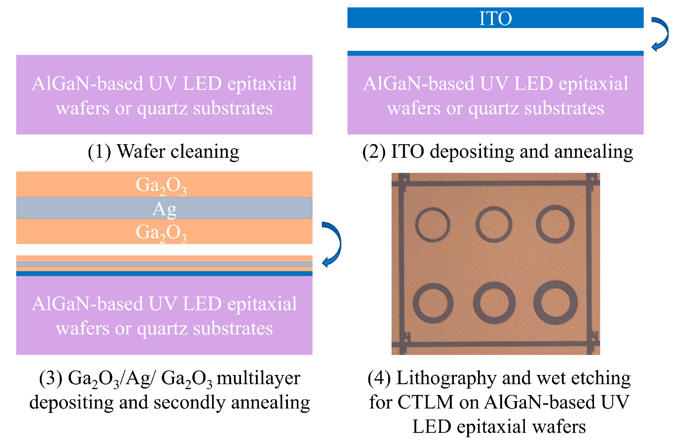
2. Materials and Methods
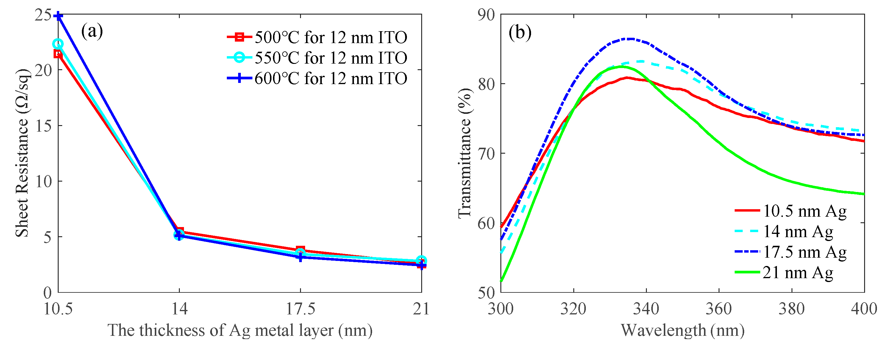
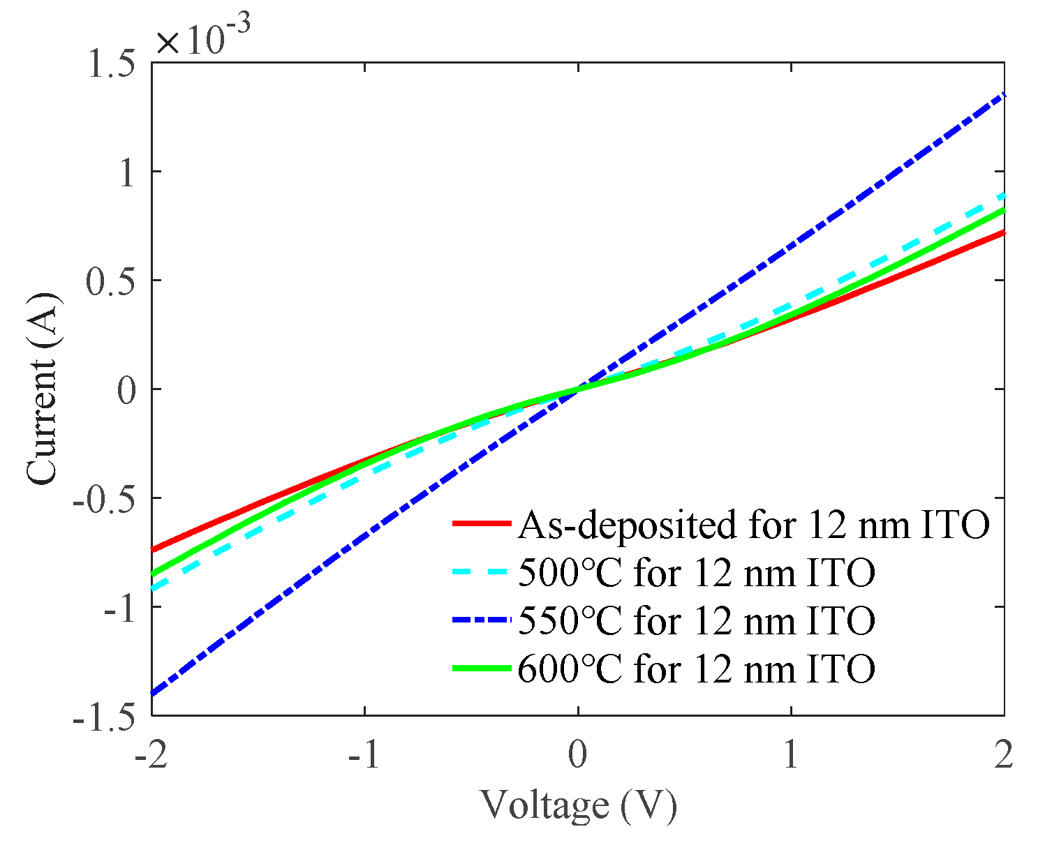
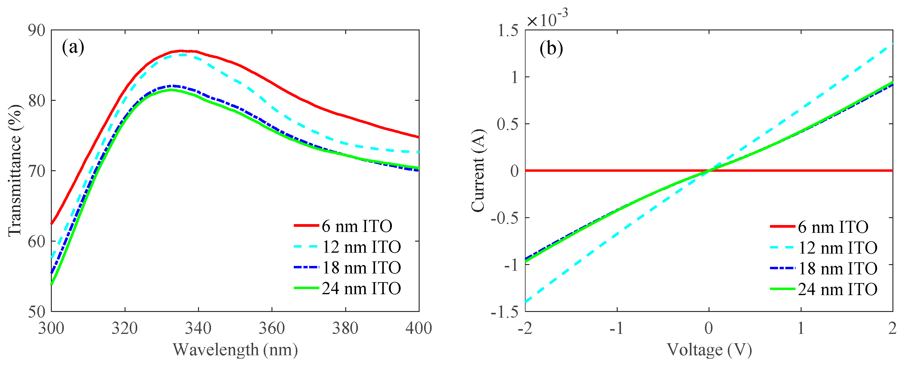
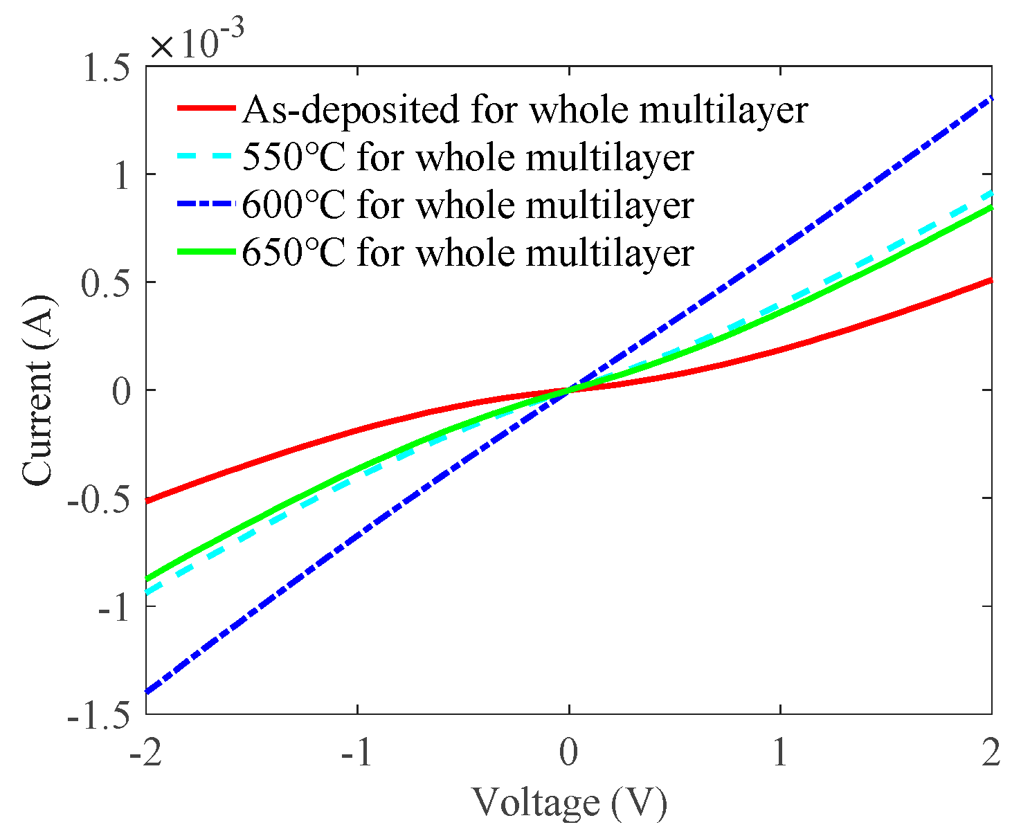
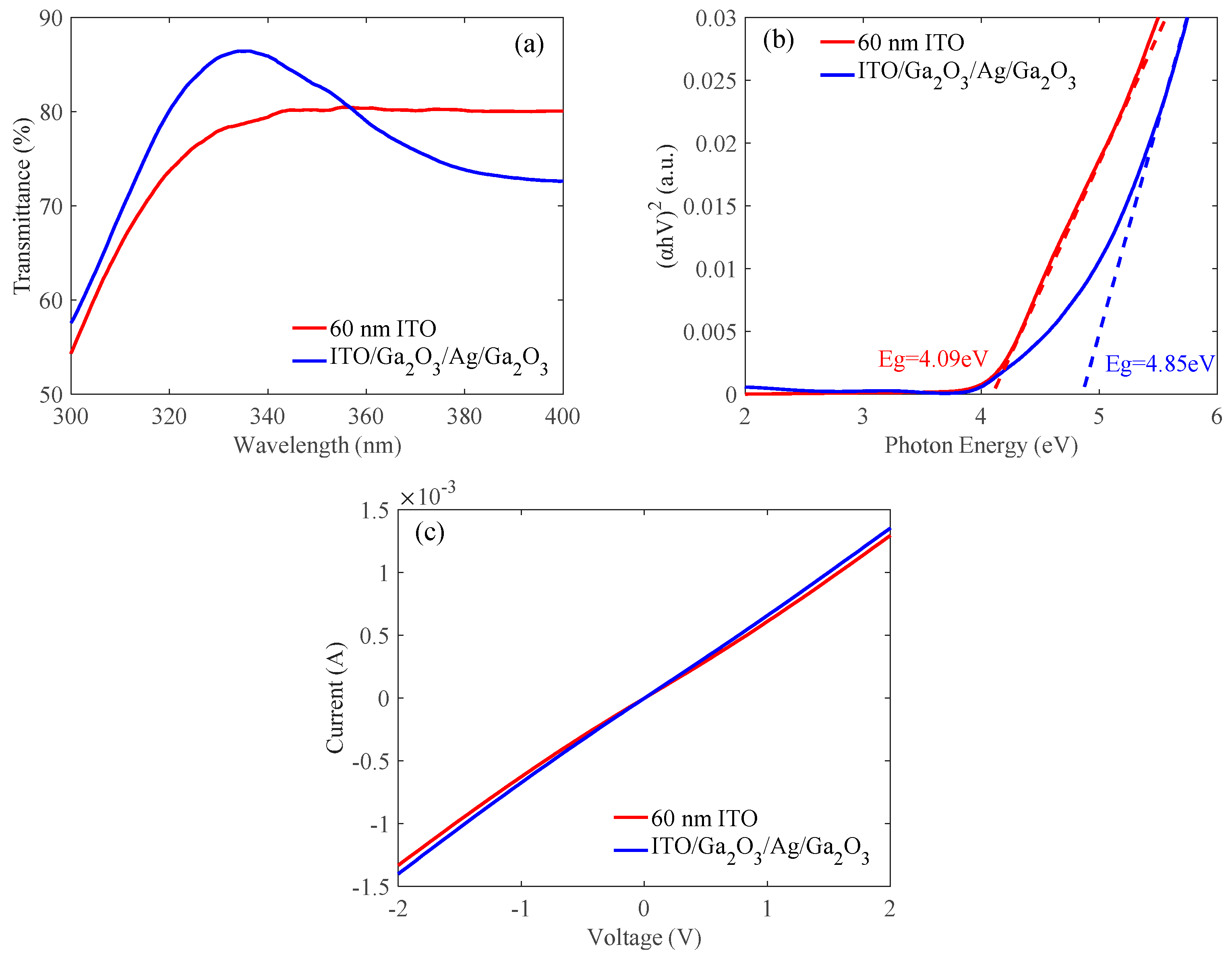
3. Results and Discussion
4. Conclusions and Further Work
Author Contributions
Funding
Conflicts of Interest
References
- Khan, A.; Balakrishnan, K.; Katona, T. Ultraviolet light-emitting diodes based on group three nitrides. Nat. Photonics 2008, 2, 77–84. [Google Scholar] [CrossRef]
- Kang, J.H.; Ryu, J.H.; Kim, H.K.; Kim, H.Y.; Han, N.; Lee, M.S.; Park, Y.J.; Uthirakumar, P.; Lysak, V.V.; Hong, C.-H. Enhancement of light output power in GaN-based light-emitting diodes using indium tin oxide films with nanoporous structures. Thin Solid Film. 2011, 520, 437–441. [Google Scholar] [CrossRef]
- Choi, J.-H.; Jang, S.-H.; Jang, J.-S. Electrical, optical, and structural characteristics of ohmic contacts between p-GaN and ITO deposited by DC-and RF-magnetron sputtering. Electron. Mater. Lett. 2013, 9, 425–428. [Google Scholar] [CrossRef]
- Hong, C.; Wie, S.; Park, M.; Kwak, J. Electron beam irradiated ITO films as highly transparent p-type electrodes for GaN-based LEDs. J. Nanosci. Nanotechnol. 2013, 13, 5420–5423. [Google Scholar] [CrossRef] [PubMed]
- Ju Chae, D.; Yoon Kim, D.; Geun Kim, T.; Mo Sung, Y.; Doeck Kim, M. AlGaN-based ultraviolet light-emitting diodes using fluorine-doped indium tin oxide electrodes. Appl. Phys. Lett. 2012, 100, 081110. [Google Scholar] [CrossRef]
- Lin, Y.H.; Liu, Y.S.; Liu, C.Y. Light Output Enhancement of Near UV-LED by Using Ti-Doped ITO Transparent Conducting Layer. IEEE Photonics Technol. Lett. 2010, 22, 1443–1445. [Google Scholar] [CrossRef]
- Kim, M.J.; Kim, T.G. Fabrication of Metal-Deposited Indium Tin Oxides: Its Applications to 385 nm Light-Emitting Diodes. ACS Appl. Mater. Interfaces 2016, 8, 5453–5457. [Google Scholar] [CrossRef] [PubMed]
- Xu, J.; Zhang, W.; Peng, M.; Dai, J.; Chen, C. Light-extraction enhancement of GaN-based 395 nm flip-chip light-emitting diodes by an Al-doped ITO transparent conductive electrode. Opt. Lett. 2018, 43, 2684–2687. [Google Scholar] [CrossRef] [PubMed]
- Cho, E.N.; Moon, P.; Chang, E.K.; Yun, I. Modeling and optimization of ITO/Al/ITO multilayer films characteristics using neural network and genetic algorithm. Expert Syst. Appl. Int. J. 2012, 39, 8885–8889. [Google Scholar] [CrossRef]
- Lee, J.H.; Woo, K.Y.; Kim, K.H.; Kim, H.D.; Kim, T.G. ITO/Ag/ITO multilayer-based transparent conductive electrodes for ultraviolet light-emitting diodes. Opt. Lett. 2013, 38, 5055–5058. [Google Scholar] [CrossRef] [PubMed]
- Jae Park, Y.; Song, H.; Deul Ryu, B.; Viet Cuong, T.; Hong, C.H. Nanostructural Effect of ZnO on Light Extraction Efficiency of Near-Ultraviolet Light-Emitting Diodes. J. Nanomater. 2016, 2016, 58. [Google Scholar]
- Park, T.Y.; Choi, Y.S.; Kang, J.W.; Jeong, J.H. Enhanced optical power and low forward voltage of GaN-based light-emitting diodes with Ga-doped ZnO transparent conducting layer. Appl. Phys. Lett. 2010, 96, 051124. [Google Scholar] [CrossRef]
- Girtan, M. Comparison of ITO/metal/ITO and ZnO/metal/ZnO characteristics as transparent electrodes for third generation solar cells. Sol. Energy Mater. Sol. Cells 2012, 100, 153–161. [Google Scholar] [CrossRef]
- Woo, K.Y.; Lee, J.H.; Kim, K.H.; Kim, S.J.; Kim, T.G. Highly transparent conductive Ag/Ga2O3 electrode for near-ultraviolet light-emitting diodes. Phys. Status Solidi 2015, 211, 1760–1763. [Google Scholar] [CrossRef]
- Woo, K.Y.; Kim, K.H.; Kim, T.G. Performance of InGaN/AlGaInN Near-UV LEDs With Ni/Ga2O3/Ag/Ga2O3 Electrode. IEEE Photonics Technol. Lett. 2016, 28, 67–70. [Google Scholar] [CrossRef]
- Kim, S.J.; Park, S.Y.; Kim, K.H.; Kim, S.W.; Kim, T.G. Ga2O3: ITO Transparent Conducting Electrodes for Near-Ultraviolet Light-Emitting Diodes. IEEE Electron Device Lett. 2014, 35, 232–234. [Google Scholar] [CrossRef]
- Seo, T.H.; Bo, K.K.; Shin, G.; Lee, C.; Kim, M.J.; Kim, H.; Suh, E.K. Graphene-silver nanowire hybrid structure as a transparent and current spreading electrode in ultraviolet light emitting diodes. Appl. Phys. Lett. 2013, 103, 051105. [Google Scholar]
- Kim, B.J.; Lee, C.; Jung, Y.; Baik, K.H.; Mastro, M.A.; Hite, J.K.; Eddy, C.R., Jr.; Kim, J. Large-area transparent conductive few-layer graphene electrode in GaN-based ultra-violet light-emitting diodes. Appl. Phys. Lett. 2011, 99, 143101. [Google Scholar] [CrossRef]
- Cho, C.Y.; Choe, M.; Lee, S.J.; Hong, S.H.; Lee, T.; Lim, W.; Kim, S.T.; Park, S.J. Near-ultraviolet light-emitting diodes with transparent conducting layer of gold-doped multi-layer graphene. J. Appl. Phys. 2013, 113, 113102. [Google Scholar] [CrossRef]
- Jeong, H.; Jeong, S.Y.; Park, D.J.; Jeong, H.J.; Jeong, S.; Han, J.T.; Jeong, H.J.; Yang, S.; Kim, H.Y.; Baeg, K.J. Suppressing spontaneous polarization of p-GaN by graphene oxide passivation: Augmented light output of GaN UV-LED. Sci. Rep. 2015, 5, 7778. [Google Scholar] [CrossRef] [PubMed]
- Tippins, H. Optical absorption and photoconductivity in the band edge of β-Ga2O3. Phys. Rev. 1965, 140, A316. [Google Scholar] [CrossRef]
- Vasyltsiv, V.I.; Rym, Y.I.; Zakharko, Y.M. Optical absorption and photoconductivity at the band edge of β-Ga2−xInxO3. Phys. Status Solidi 2010, 195, 653–658. [Google Scholar] [CrossRef]
- Ohira, S.; Suzuki, N.; Arai, N.; Tanaka, M.; Sugawara, T.; Nakajima, K.; Shishido, T. Characterization of transparent and conducting Sn-doped β-Ga2O3 single crystal after annealing. Thin Solid Film. 2008, 516, 5763–5767. [Google Scholar] [CrossRef]
- Víllora, E.G.; Shimamura, K.; Yoshikawa, Y.; Ujiie, T.; Aoki, K. Electrical conductivity and carrier concentration control in β-Ga2O3 by Si doping. Appl. Phys. Lett. 2008, 92, 202120. [Google Scholar] [CrossRef]
- Liu, J.; Yan, J.; Shi, L.; Li, T. Electrical and optical properties of deep ultraviolet transparent conductive Ga2O3/ITO films by magnetron sputtering. J. Semicond. 2010, 31, 5–9. [Google Scholar]
- Li, T.; Yan, J.; Ding, X.; Zhang, L. Effect of substrate temperature on the properties of deep ultraviolet transparent conductive ITO/Ga2O3 films. J. Semicond. 2012, 33, 013002. [Google Scholar] [CrossRef]
- Wang, H.; Zhou, Q.; Liang, S.; Wen, R. Fabrication and Characterization of AlGaN-Based UV LEDs with a ITO/Ga2O3/Ag/Ga2O3 Transparent Conductive Electrode. Nanomaterials 2019, 9, 66. [Google Scholar] [CrossRef] [PubMed]
- Guillén, C.; Herrero, J. ITO/metal/ITO multilayer structures based on Ag and Cu metal films for high-performance transparent electrodes. Sol. Energy Mater. Sol. Cells 2008, 92, 938–941. [Google Scholar] [CrossRef]
- Choi, Y.Y.; Kim, H.K.; Koo, H.W.; Kim, T.W.; Lee, S.N. Flexible ZnSnO3/Ag/ZnSnO3 multilayer electrodes grown by roll-to-roll sputtering on flexible polyethersulfone substrates. J. Vac. Sci. Technol. A Vac. Surf. Film. 2011, 29, 061502. [Google Scholar] [CrossRef]
- Fan, J.C.C.; Bachner, F.J.; Foley, G.H.; Zavracky, P.M. Transparent heat-mirror films of TiO2/Ag/TiO2 for solar energy collection and radiation insulation. Appl. Phys. Lett. 1974, 25, 693–695. [Google Scholar] [CrossRef]
- Xiaotang, L.; Zhongbin, Z.; Qing, P.; Yadong, L. Wurtzite Cu2ZnSnS4 nanocrystals: A novel quaternary semiconductor. Chem. Commun. 2011, 47, 3141–3143. [Google Scholar]
- Washizu, E.; Yamamoto, A.; Abe, Y.; Kawamura, M.; Sasaki, K. Optical and electrochromic properties of RF reactively sputtered WO3 films. Solid State Ion. 2003, 165, 175–180. [Google Scholar] [CrossRef]
- Chandramohan, S.; Kanjilal, A.; Tripathi, J.K.; Sarangi, S.N.; Sathyamoorthy, R.; Som, T. Structural and optical properties of Mn-doped CdS thin films prepared by ion implantation. J. Appl. Phys. 2009, 105, 123507. [Google Scholar] [CrossRef]


| Group | The Thickness of the ITO Contact Layer | Annealing Temperature of the ITO Contact Layer | The Thickness of the Ag Metal Layer | Annealing Temperature of the Whole ITO/Ga2O3 (15 nm)/Ag/Ga2O3 (15 nm) Multilayer |
|---|---|---|---|---|
| 1 | 12 nm | 500 °C | 10.5 nm | 600 °C |
| 550 °C | ||||
| 600 °C | ||||
| 2 | 500 °C | 14 nm | ||
| 550 °C | ||||
| 600 °C | ||||
| 3 | 500 °C | 17.5 nm | ||
| 550 °C | ||||
| 600 °C | ||||
| 4 | 500 °C | 21 nm | ||
| 550 °C | ||||
| 600 °C |
| Group | The Thickness of the ITO Contact Layer | Annealing Temperature of the ITO Contact Layer | The Thickness of the Ag Metal Layer | Annealing Temperature of the Whole ITO/Ga2O3 (15 nm)/Ag/Ga2O3 (15 nm) Multilayer |
|---|---|---|---|---|
| 1 | 6 nm | 550 °C | 17.5 nm | 600 °C |
| 2 | 12 nm | |||
| 3 | 18 nm | |||
| 4 | 24 nm |
| Group | The Thickness Of the ITO Contact Layer | Annealing Temperature of the ITO Contact Layer | The Thickness of the Ag Metal Layer | Annealing Temperature of the Whole ITO/Ga2O3 (15 nm)/Ag/Ga2O3 (15 nm) Multilayer |
|---|---|---|---|---|
| 1 | 12 nm | 550 °C | 17.5 nm | As-deposited |
| 2 | 550 °C | |||
| 3 | 600 °C | |||
| 4 | 650 °C |
| Sample | Transmittance at 335 nm | Sheet Resistance | Specific Contact Resistances |
|---|---|---|---|
| 60-nm ITO | 78.7% | 51.55 Ω/sq | 2.96×10⁻³ Ω·cm2 |
| ITO/Ga2O3/Ag/Ga2O3 | 86.4% | 3.43 Ω/sq | 1.45×10⁻³ Ω·cm2 |
© 2019 by the authors. Licensee MDPI, Basel, Switzerland. This article is an open access article distributed under the terms and conditions of the Creative Commons Attribution (CC BY) license (http://creativecommons.org/licenses/by/4.0/).
Share and Cite
Liang, S.; Zhou, Q.; Li, X.; Zhong, M.; Wang, H. Electrical and Optical Properties of a Transparent Conductive ITO/Ga2O3/Ag/Ga2O3 Multilayer for Ultraviolet Light-Emitting Diodes. Nanomaterials 2019, 9, 403. https://doi.org/10.3390/nano9030403
Liang S, Zhou Q, Li X, Zhong M, Wang H. Electrical and Optical Properties of a Transparent Conductive ITO/Ga2O3/Ag/Ga2O3 Multilayer for Ultraviolet Light-Emitting Diodes. Nanomaterials. 2019; 9(3):403. https://doi.org/10.3390/nano9030403
Chicago/Turabian StyleLiang, Siwei, Quanbin Zhou, Xianhui Li, Ming Zhong, and Hong Wang. 2019. "Electrical and Optical Properties of a Transparent Conductive ITO/Ga2O3/Ag/Ga2O3 Multilayer for Ultraviolet Light-Emitting Diodes" Nanomaterials 9, no. 3: 403. https://doi.org/10.3390/nano9030403
APA StyleLiang, S., Zhou, Q., Li, X., Zhong, M., & Wang, H. (2019). Electrical and Optical Properties of a Transparent Conductive ITO/Ga2O3/Ag/Ga2O3 Multilayer for Ultraviolet Light-Emitting Diodes. Nanomaterials, 9(3), 403. https://doi.org/10.3390/nano9030403