Article

In-Depth Characterization of Secondary Phases in Cu2ZnSnS4 Film and Its Application to Solar Cells

1
Zhongshan Institute, University of Electronic Science and Technology of China, Zhongshan 528402, China
2
State Key Laboratory of Nuclear Physics and Technology, School of Physics, Peking University, Beijing 100871, China
3
Guangdong Engineering-Technology Research Center of Nano-Photoelectric Functional Films and Devices, Zhongshan 528402, China
*
Author to whom correspondence should be addressed.
Nanomaterials 2019, 9(6), 855; https://doi.org/10.3390/nano9060855
Submission received: 16 April 2019 / Revised: 19 May 2019 / Accepted: 20 May 2019 / Published: 5 June 2019

Abstract

:
Secondary phases are common in Cu2ZnSnS4 (CZTS) thin films, which can be fatal to the performance of solar cell devices fabricated from this material. They are difficult to detect by X-Ray diffraction (XRD) because of the weak peak in spectra compared with the CZTS layer. Herein, it was found that in-depth elemental distribution by a secondary ion mass spectroscopy method illustrated uniform film composition in the bulk with slight fluctuation between different grains. X-ray photoelectron spectroscopy (XPS) measurement was conducted after sputtering the layer with different depths. An Auger electron spectrum with Auger parameter were used to check the chemical states of elements and examine the distribution of secondary phases in the CZTS films. Secondary phases of CuS, ZnS and SnS were detected at the surface of the CZTS film within a 50-nm thickness while no secondary phases were discovered in the bulk. The solar cell fabricated with the as-grown CZTS films showed a conversion efficiency of 2.1% (Voc: 514.3 mV, Jsc: 10.4 mA/cm2, FF: 39.3%) with an area of 0.2 cm2 under a 100 mW/cm2 illumination. After a 50-nm sputtering on the CZTS film, the conversion efficiency of the solar cell was improved to 6.2% (Voc: 634.0 mV, Jsc: 17.3 mA/cm2, FF: 56.9%).

1. Introduction

The kesterite Cu2ZnSn(S,Se)4 (CZTSSe) semiconductor is recognized as a promising candidate for photovoltaic applications because it uses earth abundant elements only [1,2,3]. A conversion efficiency of 12.6% has been achieved with a nonvacuum method [4]. Cu2ZnSnS4 (CZTS) has a similar structure and properties to CZTSSe but uses no toxic Se. The highest efficiency of CZTS is about 11% [5]. Currently, the efficiency of CZTS-related solar cells is still far below that of CuInGaSe2 (CIGS), which shows the highest efficiency of 23.35% [6]. One important explanation for this is the easy occurrence of secondary phases in the CZTS film due to the narrow existence region of a single kesterite phase according to the phase diagram [5]. Thus, the secondary phases are a particularly serious problem for CZTS layers.
There have been a number of studies that focus on the formation of secondary phases. Some focus on the growth mechanism of CZTS film and give explanations for the formation process of secondary phases [7,8]. Some emphasize how secondary phases affect solar cell performance [9,10]. However, reactions during the fabrication of CZTS films by the nonvacuum method can be significantly different for different approaches due to thermodynamics. Moreover, according to some reports, the secondary phases exist only on the surface of the film [11] and are difficult to detect by X-ray diffraction. It is believed that X-ray photoelectron spectroscopy (XPS) together with Auger electron spectra, because of its high sensitivity, is a good approach to detecting element chemical states.
In this work, CZTS precursors were fabricated by a nonvacuum method followed by a fast-high temperature annealing in a high-sulfur atmosphere. CZTS nanoparticle inks were obtained by a ball milling method and a spin-coating method was used to fabricate CZTS precursors. The specimens were then prepared and characterized immediately after they were taken out of the annealing chamber. To measure the element distribution in the thickness direction, secondary ion mass spectroscopy (SIMS) was conducted. XPS measurement was conducted on the sputtered CZTS films to acquire the in-depth resolved secondary phase distribution. Auger parameter was used to examine the chemical state by measuring the kinetic energies of the element. By checking the element chemical state, the distribution of secondary phases was analyzed. The as-grown film was then applied to a solar cell as the absorber layer and solar cell performance was characterized.

2. Experimental Approach

The substrate used in this work was prepared by direct current (DC) sputtering of Mo with a thickness of about 800 nm onto ultrasonically cleaned soda-lime-glass slides. The substrate was then cleaned ultrasonically to remove small particles on the surface before the fabrication of CZTS films by nanoparticle ink. The CZTS ink contains only particles less than 100 nm, which was prepared from CZTS powder by a wet ball-milling method, explained in detail in our previous paper [12]. The concentration of CZTS particles in the ink was adjusted by ethanol to 200 mg/mL. A spin coating process was used to fabricate CZTS precursors. During this process, the substrate (10 × 10 mm) rotated at a speed of 2000 rpm and CZTS ink was dripped on the surface at a speed of 5 μL/min. The obtained CZTS precursor had a thickness of 1–1.5 μm and was annealed in a sulfur atmosphere to improve the grain size and crystallinity in a 15-cm-long ampoule. To conduct CZTS annealing, sulfur powder with a purity of 99.999% was placed together with CZTS film in the ampoule at the two ends. The ampoule was evacuated to around 2.0 × 10⁻³ Pa by a diffusion pump and then sealed. Then, the sample was annealed in an annealing furnace (FP410, Yamato Company, Tokyo, Japan). The furnace temperature was monitored by a thermo sensor and the temperature of the ampoule was monitored by a thermocouple. It was found that the actual annealing temperature deviated less than 1% from the setting value. During the annealing process, the ampoule was heated to 600 °C within 15 min to achieve a high heating rate. After that, the temperature was kept at 600 °C for 20 min and then cooled naturally to around 400 °C over a period of about 15 min to provide the substrate with sulfur atmosphere protection. Then, the ampoule was removed from the annealing furnace and was allowed to cool to less than 200 °C within 5 min in a normal air environment. Then, the as-grown CZTS film was removed from the ampoule and used to conduct characterization immediately. To check the photovoltaic properties of CZTS films, the full solar cell structure was completed as follows: a 50-nm-thick CdS buffer layer was first deposited on the CZTS film by chemical bath deposition. Then, layers of metal-organic chemical vapor deposited i-ZnO (80 nm) and B-doped ZnO (600 nm). Finally, a front-contact Al grid was deposited on top via an evaporation method.
Crystallization of the CZTS film was characterized by X-ray diffraction (XRD, Rigaku, Tokyo, Japan) measurement with a 40-kV voltage and 20-mA current. The composition depth profile of the CZTS film was measured by a secondary ion mass spectrometer (TOF-SIMS, Hitachi, Tokyo, Japan), using a 3-keV primary Cs+ ion beam with a sputtering rate of 120 nm/min. To check the depth chemical states of the CZTS films, XPS measurement was conducted by an XPS spectrometer (JPS-9030, JEOL, Tokyo, Japan). An Ar+ beam generator attached to the XPS chamber was used to etch the film and the sputtering rate was adjusted to about 5 nm/min with sputtering power of 5 W. The etching rate was determined by sputtering a whole CZTS layer with a known thickness. Before measurement, the surface of the CZTS film was pre-cleaned by sputtering to clear oxidation on the surface. After the pre-clearance, the sample was defined as being in the initiate state of CZTS; that is, etching time 0 min. The sputtering time was selected as 10 min, 1 h, 3 h and 4 h, corresponding to etching depths of 50, 300, 900 and 1200 nm, respectively. After sputtering, X-ray photoelectron spectroscopy (XPS) measurement using a monochromatic Al Kα radiation source (1486.7 eV) was conducted and XPS spectra together with Auger electron spectra (AES) of the element were recorded by JPS-9030 (JEOL, Tokyo, Japan) to check the chemical state. The Mo signal in the spectrum was used to determine interface between the CZTS and Mo layers. Solar cell performance was measured with a 913 CV type current-voltage (J-V) tester (AM1.5) provided by an EKO (LP-50B, EKO, Tokyo, Japan) solar simulator. The simulator was calibrated by a standard GaAs solar cell to determine the standard illumination density (100 mW/cm2). The quantum efficiency (QE) of the CZTS solar cell was characterized by a QE-2000 tester (Otsuka Electronics Co., Ltd., Osaka, Japan).

3. Results and Discussion

3.1. Characterization of the Crystallization of a CZTS Film

To eliminate the influence of Mo on the spectra, the CZTS film was fabricated on the soda-lime glass (SLG) substrate using the method mentioned in the experimental approach (above) to carry out the XRD measurement. Figure 1 shows a representative XRD pattern of the as-grown CZTS film. In the precursor, only the main peak of kesterite CZTS can be detected [13,14] and no other expected phases, such as ternary Cu-Sn-S phases or binary Cu-S, Zn-S or Sn-S phases, are observed. The film showed a strong (112)-oriented peak, which is common in kesterite CZTS films. The result can be explained in two ways: (1) the CZTS film bulk only contains a CZTS phase and no other phases exist, thus, only peaks of the pure CZTS phase can be observed; (2) other impurity phases also exist in small amounts but are undetectable by XRD measurement or covered by the background noise. To clarify the distribution of the secondary phases, further measurement must be conducted.

3.2. In-Depth Elemental Distribution in a CZTS Film

Figure 2 illustrates in-depth elemental distribution profiles of a CZTS film by a SIMS method. The yellow area in the figure indicates the interface of the CZTS and Mo layer based on the following: (1) the concentration of Cu, Zn, Sn and S decreased abruptly; (2) the concentration of the Mo element increased significantly. Judging from the figure, the Cu, Zn, Sn and S elements distribute uniformly with small fluctuations in the CZTS bulk. No significant segregation of any element is detected. The fluctuation of elemental distribution is referred to as composition variation between grains. However, all elements show a relatively high concentration near both the front and back surfaces of the CZTS film, indicating relatively high concentrations. The distribution of elements near the front surface is explained by the distribution of secondary phases according to our experimental result in the following section. However, the reason for the high elemental distribution near the back surface remains unknown in our case but a possible explanation is element precipitation. The segregation of S near the CZTS/Mo interface is due to the formation of MoS2, which has been widely reported. The concentration of Na gradually increases from the front surface to the back surface of the CZTS film, illustrating the diffusion profile of Na during the fabrication process.

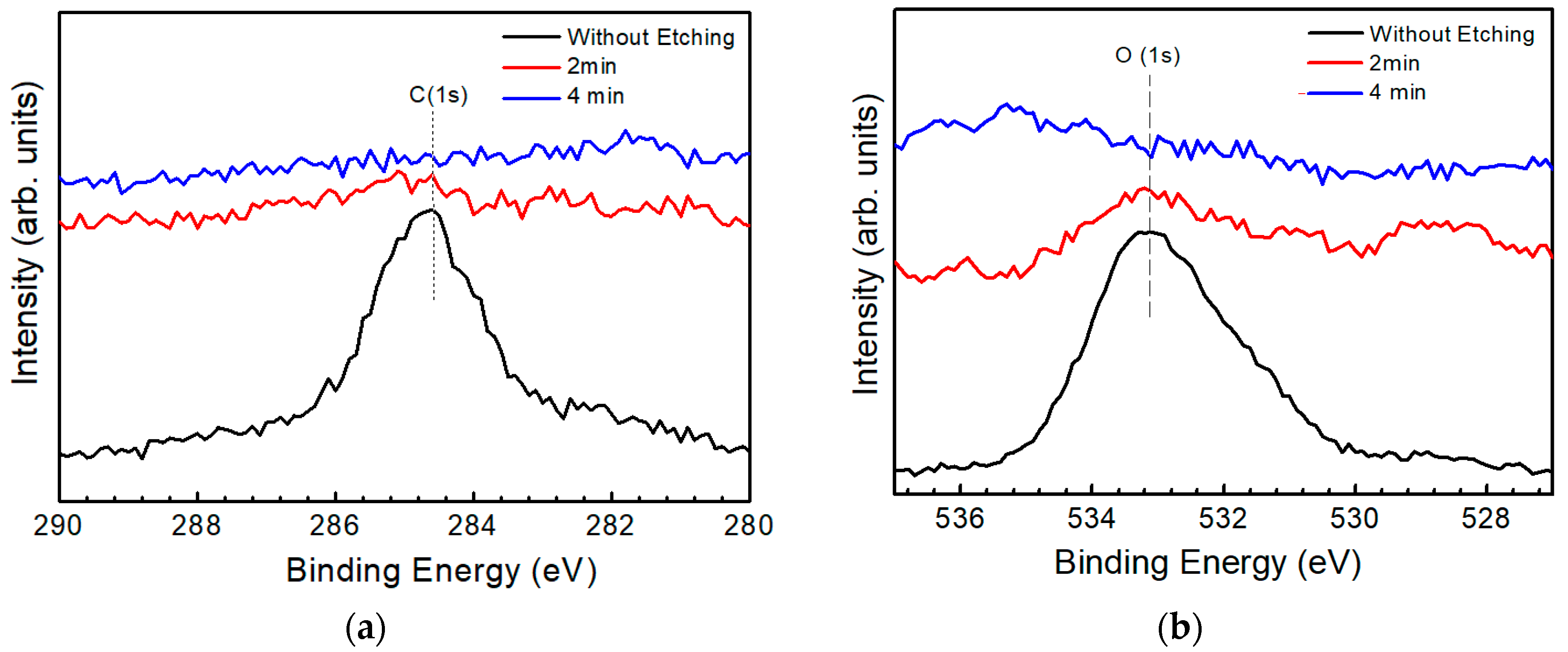
3.3. Identification of a Secondary Phase by XPS

Figure 3a,b show the XPS spectra for C and O, respectively, using a binding energy of 284.6 eV of C as the reference to rectify the spectra. The peak at a binding energy of around 284.6 eV is a typical peak of chemisorbed carbon, while a peak at around 532 eV is a typical peak of chemisorbed oxygen [15]. Judging from the figure, C and O atoms mainly exist on the surface of the as-grown CZTS film because of the adsorption effect. As the film was sputtered to a thickness of 10 nm (sputtering time 2 min), the XPS spectrum intensity for both O and C decreased dramatically and no obvious peak was detected, indicating the disappearance of C and O atoms. Adsorption of O and C atoms on the surface was an explanation for the result.
For the following sections, samples after surface cleaning to remove oxygen, as explained in the previous section, are defined as initial state of the sample; that is, ‘etching time 0 min.’ Figure 4a shows the XPS spectra for Cu 2p3/2 in the CZTS film with etching times of 0 min (without etching), 10 min (50 nm), 1 h (300 nm), 3 h (900 nm) and 4 h (1.2 μm). A single peak around 932.2 eV was observed for all samples and with an increase in etching time, the peak shifted slightly toward a higher binding energy. When the etching time is less than 3 hours, XPS spectra show strong peaks indicating a large amount of Cu compounds. When the sample is etched for 4 hours, the peaking intensity decreases dramatically, which is used to determine the back surface of the CZTS film. During the annealing process for CZTS, secondary phases form easily because of the decomposition of the CZTS films [16]. It is reported that the binding energies of Cu 2p3/2 for possible Cu compounds in CZTS film are 932.6 eV for Cu2S, 932.5 eV for CuS and 932.2 eV for CZTS [17] and the binding energies of different chemical states are illustrated in Figure 4a. However, it is difficult to determine the chemical state in the film by XPS spectra (as shown in Figure 4a) because of small differences in the binding energies for different compounds. Therefore, Auger spectra of Cu LMM is also acquired with the same CZTS film used to conduct XPS spectra, as shown in Figure 4b.
An Auger parameter cancels the influences of electrical charging at the surface and combines the effects of XPS and AES analysis. Thus, it is effective for separating peaks with similar binding energies in the XPS spectra. Calculation of an Auger parameter is shown in Equation (1) [18].
Auger Parameter α = Binding Energy + Kinetic Energy,
The binding energy (BE) is obtained from the XPS spectra of an element while the kinetic energy (KE) is calculated from the Auger spectra of the element. It is important to state that the BE and KE are both referred to as the Fermi level.
In the case of Cu,
αCu = BE(Cu 2p3/2) + [hυ−E(A-Cu LMM)],
where BE(Cu 2p3/2) is the peak energy of Cu 2p3/2 in the XPS spectra, hυ is the X-ray energy of Al Kα (1486.6 eV) and E(A-Cu LMM) is the peak position of the Auger spectra of Cu LMM.
Figure 5 shows the Auger parameters of Cu in Cu metal, CZTS and CuS compounds. In the figure, dashed lines represent Auger parameters with an interval of 1 eV. The ( Nanomaterials 09 00855 i001), ( Nanomaterials 09 00855 i002), ( Nanomaterials 09 00855 i003) and ( Nanomaterials 09 00855 i004) symbols represent reference data of the Cu metal, Cu2S, CuS and CZTS film [19,20,21], respectively. The ( Nanomaterials 09 00855 i005) and ( Nanomaterials 09 00855 i006) symbols are experimental data of the surface and the bulk, respectively. The Auger parameter of Cu on the surface is quite different from that in the bulk. The parameter of Cu on the surface is near CuS in the CZTS film, while in the bulk it is near CZTS. The result indicates that the surface of the CZTS film is covered by a secondary phase of CuS and no such phase is observed in the CZTS bulk.
It is reported that the Zn element in the ZnS compound shows a binding energy of 1022 eV [22] and that in pure CZTS, it is around 1022 eV as well [23]. Figure 6a shows the XPS spectra for Zn 2p3/2 in a CZTS film with different etching time. Dashed lines in the figure illustrate peak position of the spectra. XPS spectra shows a peak around 1022.8 eV for the surface (etching time: 0 min) and peaks around 1021.4 eV in the bulk, corresponding to ZnS and CZTS, respectively. Thus, it is inferred that the surface of CZTS film is covered by secondary phase of ZnS and no ZnS phase is detected in the CZTS bulk. To further confirm the result, Auger spectra of Zn LMM is acquired with the same CZTS film used to conduct XPS spectra, as shown in Figure 6b.
In the case of Zn, the Auger parameter is calculated as [24]:
αZn = BE(Zn 2p3/2) + [hυ−E(A-Zn LMM)],
where the E(A-Zn LMM) is the binding energy of the Auger electron spectra, as shown in Figure 6a.
Figure 7 shows the Auger parameters of Zn in Zn metal, CZTS and ZnS compounds. In the figure, dashed lines represent Auger parameters with an interval of 1 eV. The ( Nanomaterials 09 00855 i013), ( Nanomaterials 09 00855 i014) and ( Nanomaterials 09 00855 i015) symbols correspond to reference data of Zn metal, ZnS and CZTS film [25,26,27], respectively. The ( Nanomaterials 09 00855 i016) and ( Nanomaterials 09 00855 i017) symbols are experimental data of the surface and the bulk, respectively. Judging from the figure, the Auger parameter of Zn on the surface is nearly that of ZnS, while in the bulk it is nearly that of CZTS. The result indicates that the secondary phase of ZnS mainly exists on the surface and in the bulk, ZnS is not detected, which is consistent with a previous result.
Figure 8a shows the XPS spectra for Sn3d3/2 in a CZTS film with different etching times. Dashed lines indicate the peak positions of possible SnS compounds in CZTS films. Binding energies of 485.8, 485.5, 486.5 and 486.3 eV correspond to Sn2S3, SnS, SnS2 and CZTS [28,29], respectively. Although identification of the chemical state in the film is difficult because of the small differences between the binding energies of different peaks, it is clear that chemical states at the surface and in the bulk of CZTS are different. The XPS spectra show a main peak around 485.8 eV at the surface and peaks around 486.0 eV under the surface. Therefore, it is inferred that the surface of the CZTS bulk is covered by a thin layer of an SnS compound. To further confirm our conclusion, Auger electron spectra was acquired, as shown in Figure 8b.
In the case of Sn, the Auger parameter is calculated as [30]:
αSn = BE(Sn 3d5/2) + [hυ−E(A-Sn MNN)],
where, E(A-Sn MNN) is the binding energy of Sn 3d5/2 obtained from the Auger electron spectra. The reference Auger parameter of Sn in different chemical states and the experimental data in our CZTS film are drawn together in Figure 9. Dashed lines in the figure represent Auger parameters with an interval of 1 eV. The ( Nanomaterials 09 00855 i023), ( Nanomaterials 09 00855 i024), ( Nanomaterials 09 00855 i025), ( Nanomaterials 09 00855 i026) and ( Nanomaterials 09 00855 i027) symbols represent the reference data of Sn metal, SnS, Sn2S3 and CZTS in a CIGS film [25,29,31], respectively. The ( Nanomaterials 09 00855 i028) and ( Nanomaterials 09 00855 i029) symbols are the experimental data of the surface and the bulk, respectively. The Auger parameter of Sn on the surface is nearly that of the SnS compound, while in the bulk it is nearly that of CZTS, Sn2S3 and SnS2. According to the XRD result, the main structure of the film is CZTS, which shows that the bulk is CZTS but not an SnS compound. Thus, it can be concluded that the surface of the CZTS film is covered by a secondary phase of SnS but no such secondary phase is observed in the bulk, which accords with our previous result. Although it has also been reported that ternary compounds such as Cu2SnS3 and Cu3SnS4 may also exist on the surface [32], they were not identified in the XPS spectra in this work.
Figure 10 shows a schematic of the growth process of a CZTS film. During annealing, the grain size of the CZTS film gradually grows and secondary phases precipitate on the surface of the film. The total thickness of the secondary phase layer is several tens of nanometers and consists of CuS, ZnS and SnS compounds.
To improve CZTS/CdS interface quality, the CZTS film was etched for 10 min (50 nm), aiming at reducing the influence of the secondary phase on solar cell performance. The CZTS films before and after etching were fabricated with other layers to complete the solar cell structures. Solar cell performance was evaluated under standard conditions with an irradiation of 100 mW/cm2. The intensity of the solar simulator was calibrated by a high-precision monocrystalline Si solar cell to achieve a standard illumination. Figure 11 shows the J-V curve of CZTS solar cells and the area was 0.2 cm2. The photovoltaic device without etching exhibited a conversion efficiency of 2.1%, with open circuit voltage (Voc) = 514.3 mV, short circuit current density (Jsc) = 10.4 mA/cm2 and fill factor (FF) = 39.3%. For the CZTS absorber with etching, the solar cell showed an efficiency of 6.2%, with Voc = 633.3 mV, Jsc = 17.3 mA/cm2 and FF = 56.9%.
Figure 12 shows the external quantum efficiency (EQE) curve of the CZTS solar cell. After etching, the QE was significantly improved, as shown in the figure. The QE curve exhibits an abrupt drop in the infrared region around 770 nm, which was the CZTS absorption edge. Thus, the calculated bandgap of the CZTS films was about 1.61 eV. The features near 510 and 380 nm corresponded to the absorption edges of the CdS and ZnO layers [33], respectively, which was common when using the respective CdS buffer and ZnO window layers. Based on the EQE data of a solar cell, Jsc was calculated as [34]:
J s c = q 0 Q E ( E ) b s ( E , T s ) d E
where, q is the elementary charge, QE is quantum efficiency and bs is solar flux or irradiation. For air mass 1.5, the data are available from Ref. [35]. Based on Equation (5), Figure 12 and the solar irradiation spectrum, Jsc, of the CZTS solar cell was calculated as 8.4 mA/cm2 for a CZTS solar cell without etching and 15.5 mA/cm2 for a solar cell with etching. Because the J-V curve represents the real performance of a photovoltaic device, the slight deviation of Jsc calculated from the QE curve can be explained as follows: the QE measurement is carried out at a single wavelength with much lower intensity than that of a one sun irradiation.

4. Conclusions

A CZTS film was obtained by annealing a CZTS nanoparticle precursor in an S atmosphere. Elemental distribution of the film was uniform with slight fluctuation judging from the SIMS result. Secondary phases that could not be distinguished by XRD based techniques were identified by an XPS measurement. In-depth chemical states of elements were checked by combing Auger electron spectra and an Auger parameter at different depths of the film. When CZTS films were annealed in the S atmosphere, the surface of the films existed a secondary phase layer composed of CuS, ZnS and SnS while the whole film below the surface was in a CZTS phase. To remove the secondary phase, the CZTS film was etched to a depth of 50 nm and fabricated with other layers to complete the solar cell structure. The conversion efficiency of the CZTS solar cell was improved from 2.1% (Voc: 514.3 mV, Jsc: 10.4 mA/cm2, FF: 39.3%, area: 0.2 cm2) to 6.2% (Voc: 634.0 mV, Jsc: 17.3 mA/cm2, FF: 56.9%, area: 0.2 cm2) under standard solar illumination.

Author Contributions

Conceptualization: X.Z.; Part of the characterization: E.F.; Funding acquisition: Y.W.; Draft review and editing: H.W.

Funding

Part of the work was financially supported by a Grant for Special Research Projects of Zhongshan Institute (Funding No. 417YKQ10). This work was also financially supported by the National Science Foundation of China (Grant Nos. 61302044 and 61671140).

Conflicts of Interest

The authors declare no conflict of interest.

References

  1. Park, S.N.; Sung, S.J.; Son, D.H.; Kim, D.H.; Gansukh, M.; Cheong, H.; Kang, J.K. Solution-processed Cu2ZnSnS4 Absorbers Prepared by Appropriate Inclusion and Removal of Thiourea. RSC Adv. 2014, 4, 9118–9125. [Google Scholar] [CrossRef]
  2. Su, Z.H.; Tan, J.M.R.; Li, X.L.; Zeng, X.; Batabyal, S.K.; Wong, L.H. Cation Substitution of Solution-Processed Cu2ZnSnS4 Thin Film Solar Cell with over 9% Efficiency. Adv. Energy Mater. 2015, 5, 1500682. [Google Scholar] [CrossRef]
  3. Hadke, S.H.; Levcenko, S.; Lie, S.; Hages, C.J.; Márquez, J.A.; Unold, T.; Wong, L.H. Synergistic Effects of Double Cation Substitution in Solution-Processed CZTS Solar Cells with over 10%. Adv. Energy Mater. 2018, 8, 1802540. [Google Scholar] [CrossRef]
  4. Wang, W.; Winkler, M.T.; Gunawan, O.; Gokmen, T.; Todorov, T.K.; Zhu, Y.; Mitzi, D.B. Device Characteristics of CZTSSe Thin-Film Solar Cells with 12.6% Efficiency. Adv. Energy Mater. 2014, 4, 1301465. [Google Scholar] [CrossRef]
  5. Akhavan, V.A.; Goodfellow, B.W.; Panthani, M.G.; Steinhagen, C.; Harvey, T.B.; Stolle, C.J.; Korgel, B. Colloidal CIGS and CZTS Nanocrystals: A Precursor Route to Printed Photovoltaics. J. Solid State Chem. 2012, 189, 2–12. [Google Scholar] [CrossRef]
  6. Yoshida, S. Solar Frontier Achieves World Record Thin-Film Solar Cell Efficiency of 23.35%. Available online: http://www.solar-frontier.com/eng/news/2019/0117_press.html (accessed on 17 January 2019).
  7. Garcia-Llamas, E.; Merino, J.M.; Gunder, R.; Neldner, K.; Greiner, D.; Steigert, A.; Giraldo, S.; Izquierdo-Roca, V.; Saucedo, E.; León, M.; et al. Cu2ZnSnS4 Thin Film Solar Cells Grown by Fast Thermal Evaporation and Thermal Treatment. Sol. Energy 2017, 141, 236–241. [Google Scholar] [CrossRef]
  8. Kermadia, S.; Sali, S.; Zougar, L.; Boumaour, M.; Gunder, R.; Schorr, S.; Izquierdo-Roca, V.; Pérez-Rodríguez, A. An In-depth Investigation on the Grain Growth and the Formation of Secondary Phases of Ultrasonic-sprayed Cu2ZnSnS4 based Thin Films Assisted by Na Crystallization Catalyst. Sol. Energy 2018, 176, 277–286. [Google Scholar] [CrossRef]
  9. Babichuk, I.S.; Golovynskyi, S.; Brus, V.V.; Babichuk, I.V.; Datsenko, O.; Li, J.; Xu, G.W.; Golovynska, I.; Hreshchuk, O.M.; Orletskyi, I.G.; et al. Secondary Phases in Cu2ZnSnS4 Films Obtained by Spray Pyrolysis at different Substrate Temperatures and Cu Contents. Mater. Lett. 2018, 216, 173–175. [Google Scholar] [CrossRef]
  10. Just, J.; Lützenkirchen-Hecht, D.; Müller, O.; Frahm, R.; Unold, T. Depth Distribution of Secondary Phases in Kesterite Cu2ZnSnS4 by Angle-resolved X-ray Absorption Spectroscopy. APL Mater. 2017, 5, 126106. [Google Scholar] [CrossRef]
  11. Scragg, J.J.; Ericson, T.; Kubart, T.; Edoff, M.; Platzer-Björkman, C. Chemical Insights into the Instability of Cu2ZnSnS4 Films during Annealing. Chem. Mater. 2011, 23, 4625–4633. [Google Scholar] [CrossRef]
  12. Zhang, X.F.; Fu, E.G.; Wang, Y.H.; Zhang, C. Fabrication of Cu2ZnSnS4 (CZTS) Nanoparticle Inks for Growth of CZTS Films for Solar Cells. Nanomaterials 2019, 9, 336. [Google Scholar] [CrossRef] [PubMed]
  13. Schmidt, J.; Roscher, H.H.; Labusch, R. Preparation and Properties of CuInSe2 Thin Films Produced by Selenization of Co-sputtered Cu-In films. Thin Solid Films 1994, 251, 116–120. [Google Scholar] [CrossRef]
  14. Khare, A.; Himmetoglu, B.; Cococcioni, M.; Aydil, E.S. First Principles Calculation of the Electronic Properties and Lattice Dynamics of Cu2ZnSn(S1−xSex)4. J. Appl. Phys. 2012, 111, 123704. [Google Scholar] [CrossRef]
  15. Prabhakaran, K.; Rao, C.N.R. A Combined EELS-XPS Study of Molecularly Chemisorbed Oxygen on Silver Surfaces: Evidence for Superoxo and Peroxo Species. Surf. Sci. 1987, 186, L575–L580. [Google Scholar] [CrossRef]
  16. Awadallah, O.; Cheng, Z. Study of the Fundamental Phase Formation Mechanism of Sol-gel Sulfurized Cu2ZnSnS4 Thin Films using in situ Raman Spectroscopy. Sol. Energy Sol. Cell 2018, 176, 222–229. [Google Scholar] [CrossRef]
  17. Tao, J.H.; Liu, J.F.; Chen, L.L.; Cao, H.Y.; Meng, X.K.; Zhang, Y.B.; Zhang, C.J.; Sun, L.; Yang, P.X.; Chu, J.H. 7.1% Efficient Co-electroplated Cu2ZnSnS4 Thin Film Solar Cells with Sputtered CdS Buffer Layers. Green Chem. 2016, 18, 550–557. [Google Scholar] [CrossRef]
  18. Caporali, S.; Tolstogouzov, A.; Teodoro, O.M.N.D.; Innocenti, M.; Benedetto, F.D.; Cinotti, S.; Picca, R.A.; Sportelli, M.C.; Cioffi, N. Sn-deficiency in the Electrodeposited Ternary CuxSnySz Thin Films by ECALE. Sol. Energy Mater. Sol. Cell 2015, 138, 9–16. [Google Scholar] [CrossRef]
  19. Nakai, I.; Sugitani, Y.; Nagashima, K.; Niwa, Y. X-ray Photoelectron Spectroscopic Study of Copper Minerals. J. Inorg. Nucl. Chem. 1978, 40, 789–791. [Google Scholar] [CrossRef]
  20. Cabrera-German, D.; García-Valenzuela, J.A.; Martínez-Gil, M.; Suárez-Campos, G.; Montiel-González, Z.; Sotelo-Lerma, M.; Cota-Leal, M. Assessing the chemical state of chemically deposited copper sulfide: A quantitative analysis of the X-ray photoelectron spectra of the amorphous-to-covellite transition phases. Appl. Surf. Sci. 2019, 481, 281–295. [Google Scholar] [CrossRef]
  21. Biesinger, M.C. Advanced Analysis of Copper X-ray Photoelectron Spectra. Surf. Interface Anal. 2017, 49, 1325–1334. [Google Scholar] [CrossRef]
  22. Tao, J.H.; Chen, L.L.; Cao, H.Y.; Zhang, C.J.; Liu, J.F.; Zhang, Y.B.; Huang, L.; Jiang, J.C.; Yang, P.X.; Chu, J.H. Co-electrodeposited Cu2ZnSnS4 Thin-Film Solar Cells with over 7% Efficiency Fabricated via Fine-tuning of the Zn Content in Absorber Layers. J. Mater. Chem. A 2016, 4, 3798–3805. [Google Scholar] [CrossRef]
  23. Ge, S.J.; Gao, H.; Hong, R.J.; Li, J.J.; Mai, Y.H.; Lin, X.Z.; Yang, G.W. Improvement of Cu2ZnSn(S,Se)4 Solar Cells by Adding N,N-Dimethylformamide to the Dimethyl Sulfoxide-Based Precursor Ink. ChemSusChem 2019, 12, 1692–1699. [Google Scholar] [CrossRef] [PubMed]
  24. Winiarski, J.; Tylus, W.; Szczygie, B. EIS and XPS Investigations on the Corrosion Mechanism of Ternary Zn-Co-Mo Alloy Coatings in NaCl Solution. Appl. Surf. Sci. 2016, 364, 455–466. [Google Scholar] [CrossRef]
  25. Powell, C.J. Recommended Auger Parameters for 42 Elemental Solids. J. Electron Spectrosc. 2012, 185, 1–3. [Google Scholar] [CrossRef]
  26. Deroubaix, G.; Marcus, P. X-ray Photoelectron Spectroscopy Analysis of Copper and Zinc Oxides and Sulphides. Surf. Interface Anal. 1992, 18, 39–46. [Google Scholar] [CrossRef]
  27. Langer, D.W.; Vesely, C.J. Electronic Core Levels of Zinc Chalcogenides. Phys. Rev. B 1970, 2, 4885–4892. [Google Scholar] [CrossRef]
  28. Lin, A.W.C.; Armstrong, N.R.; Kuwana, T. X-ray Photoelectron/Auger Electron Spectroscopic Studies of Tin and Indium Metal Foils and Oxides. Anal. Chem. 1977, 49, 1228–1235. [Google Scholar] [CrossRef]
  29. Cruz, M.; Morales, J.; Espinos, J.P.; Sanz, J. XRD, XPS and Sn NMR Study of Tin Sulfides Obtained by Using Chemical Vapor Transport Methods. J. Solid State Chem. 2003, 175, 359–365. [Google Scholar] [CrossRef]
  30. Kövér, L.; Moretti, G.; Kovács, Z.; Sanjinés, R.; Cserny, I.; Margaritondo, G.; Pálinkás, J.; Adachi, H. High Resolution Photoemission and Auger Parameter Studies of Electronic Structure of Tin Oxides. J. Vac. Sci. Technol. A 1995, 13, 1382–1388. [Google Scholar] [CrossRef]
  31. Lee, J.Y.; Kim, I.Y.; Surywanshi, M.P.; Ghorpade, U.V.; Lee, D.S.; Kim, J.H. Fabrication of Cu2SnS3 Thin Film Solar Cells using Cu/Sn Layered Metallic Precursors Prepared by a Sputtering Process. Sol. Energy. 2017, 145, 27–32. [Google Scholar] [CrossRef]
  32. Fontané, X.; Calvo-Barrio, L.; Izquierdo-Roca, V.; Saucedo, E.; Pérez-Rodriguez, A.; Morante, J.R.; Berg, D.M.; Dale, P.J.; Siebentritt, S. In-depth Resolved Raman Scattering Analysis for the Identification of Secondary Phases: Characterization of Cu2ZnSnS4 Layers for Solar Cell Applications. Appl. Phys. Lett. 2011, 98, 181905. [Google Scholar] [CrossRef]
  33. Ramanathan, K.; Contreras, M.A.; Perkins, C.L.; Asher, S.; Hasoon, F.S.; Keane, J.; Young, D.; Romero, M.; Metzger, W.; Noufi, R.; et al. Properties of 19.2% Efficiency ZnO/CdS/CuInGaSe2 Thin-Film Solar Cells. Prog. Photovolt. 2003, 11, 225–230. [Google Scholar] [CrossRef]
  34. Abous-Ras, D.; Kirchartz, T.; Rau, U. Advanced Characterization Techniques for Thin Film Solar Cells, 1st ed.; WILEY-VCH Verlag GmbH&Co. KGaA: Weinheim, Germany, 2011; p. 6. [Google Scholar]
  35. Christians, J.A.; Manser, J.S.; Kamat, P.V. Best Practices in Perovskite Solar Cell Efficiency Measurements. Avoiding the Error of Making Bad Cells Look Good. J. Phys. Chem. Lett. 2015, 6, 852–857. [Google Scholar] [CrossRef] [PubMed]
Figure 1. X-ray diffraction (XRD) pattern of a typical Cu2ZnSnS4 (CZTS) film.
Nanomaterials 09 00855 g001
Figure 2. Depth profiles of elements in a CZTS film by secondary ion mass spectroscopy (SIMS) characterization for Mo, Na, Cu, Zn, Sn and S.
Nanomaterials 09 00855 g002
Figure 3. X-ray photoelectron spectroscopy (XPS) spectra of (a) carbon and (b) oxygen measured at different depths from a CZTS thin film: surface (without etching), 10 nm (2 min), 20 nm (4 min). The spectrum of C was used as the reference and all the peaks were rectified according to the peak of C at a binding energy of 284.6 eV.
Nanomaterials 09 00855 g003
Figure 4. (a) XPS spectra of Cu 2p3/2 and (b) Auger electron spectra of the Cu LMM of a CZTS film. Dotted lines in (a) indicate the peak positions of Cu2S, CuS and CZTS and in (b) indicate peak positions of the spectra.
Nanomaterials 09 00855 g004
Figure 5. Auger parameters of Cu in Cu metal, CZTS and CuS compounds. The ( Nanomaterials 09 00855 i007), ( Nanomaterials 09 00855 i008), ( Nanomaterials 09 00855 i009) and ( Nanomaterials 09 00855 i010) symbols show the reference data of Cu metal, Cu2S, CuS and CZTS in the CZTS film, respectively. The ( Nanomaterials 09 00855 i011) symbol shows the experimental data on the surface in this work. ( Nanomaterials 09 00855 i012) shows the experimental data of the CZTS in the bulk.
Nanomaterials 09 00855 g005
Figure 6. (a) XPS spectra of Zn 2p3/2 and (b) Auger electron spectra of Zn LMM of a CZTS film. Dotted lines in (a) indicate the peak positions of ZnS and CZTS and in (b) indicate the peak positions of the spectra.
Nanomaterials 09 00855 g006
Figure 7. Auger parameters of Zn in Zn metal, CZTS and ZnS compounds. The ( Nanomaterials 09 00855 i018), ( Nanomaterials 09 00855 i019) and ( Nanomaterials 09 00855 i020) symbols show reference data of Zn metal, ZnS and CZTS in CZTS film, respectively. The ( Nanomaterials 09 00855 i021) symbol shows experimental data on the surface in this work. ( Nanomaterials 09 00855 i022) shows experimental data in the bulk of a CZTS film.
Nanomaterials 09 00855 g007
Figure 8. (a) XPS spectra of Sn 3d3/2 and (b) Auger electron spectra of Sn MNN of a CZTS film. The dotted lines in (a) indicate peak positions of Sn in SnS compounds and CZTS and in (b) indicate peak positions of the Auger electron spectra.
Nanomaterials 09 00855 g008
Figure 9. Auger parameters of Sn in Sn metal, CZTS and SnS compounds. The ( Nanomaterials 09 00855 i030), ( Nanomaterials 09 00855 i031), ( Nanomaterials 09 00855 i032) ( Nanomaterials 09 00855 i033) and ( Nanomaterials 09 00855 i034) symbols show the reference data of Sn metal, SnS, Sn2S3, SnS2 and CZTS in a CZTS film, respectively. The ( Nanomaterials 09 00855 i035) symbol shows experimental data on the surface in this work. ( Nanomaterials 09 00855 i036) shows experimental data in the bulk of a CZTS film.
Nanomaterials 09 00855 g009
Figure 10. Schematic of the CZTS growth process and formation of secondary phases.
Nanomaterials 09 00855 g010
Figure 11. J-V curve of CZTS solar cells (a) without etching (b) etching for 10 min.
Nanomaterials 09 00855 g011
Figure 12. Quantum efficiency of CZTS solar cells (a) without etching (b) etching for 10 min.
Nanomaterials 09 00855 g012

