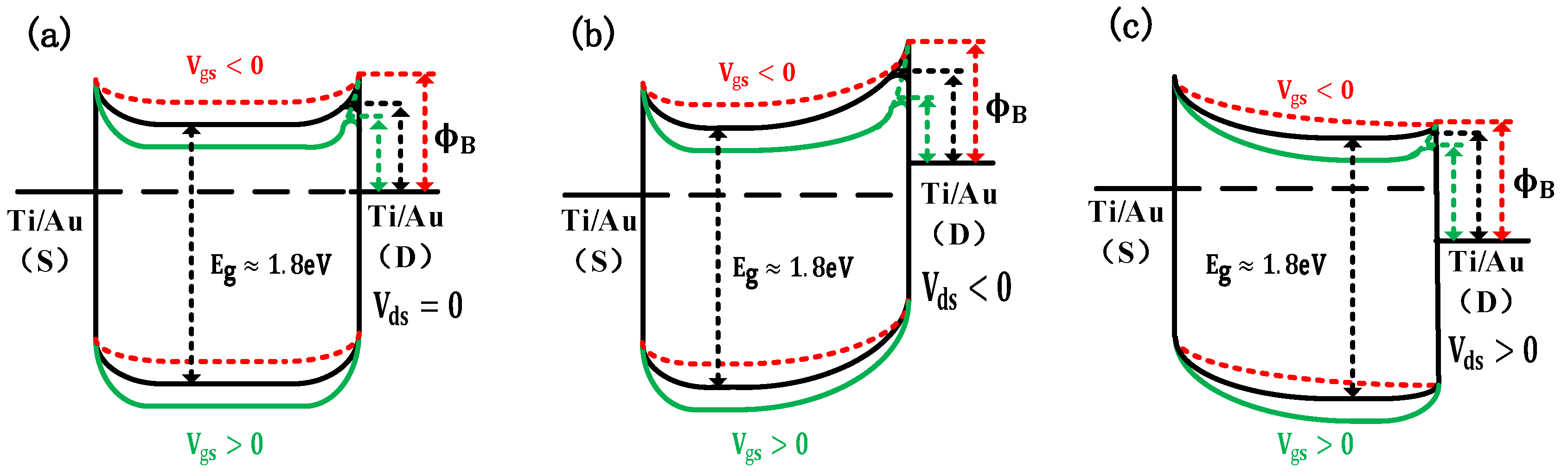
A Horizontal-Gate Monolayer MoS2 Transistor Based on Image Force Barrier Reduction


Abstract
Share and Cite
Yang, K.; Liu, H.; Wang, S.; Li, W.; Han, T. A Horizontal-Gate Monolayer MoS2 Transistor Based on Image Force Barrier Reduction. Nanomaterials 2019, 9, 1245. https://doi.org/10.3390/nano9091245
Yang K, Liu H, Wang S, Li W, Han T. A Horizontal-Gate Monolayer MoS2 Transistor Based on Image Force Barrier Reduction. Nanomaterials. 2019; 9(9):1245. https://doi.org/10.3390/nano9091245
Chicago/Turabian StyleYang, Kun, Hongxia Liu, Shulong Wang, Wei Li, and Tao Han. 2019. "A Horizontal-Gate Monolayer MoS2 Transistor Based on Image Force Barrier Reduction" Nanomaterials 9, no. 9: 1245. https://doi.org/10.3390/nano9091245
APA StyleYang, K., Liu, H., Wang, S., Li, W., & Han, T. (2019). A Horizontal-Gate Monolayer MoS2 Transistor Based on Image Force Barrier Reduction. Nanomaterials, 9(9), 1245. https://doi.org/10.3390/nano9091245