Abstract
This study investigated the shielding effectiveness (SE) of glass materials with conductive coatings by establishing a 3000 × 3000 × 3000 mm electromagnetic pulse (EMP)—shielded room according to the EMP shielding requirements in the US military standard MIL-STD-188-125-1. The EMP SE of conductive-coated glass samples was measured and verified with the broadband EMP conditions of 10 kHz∼1 GHz. The conductive thin film coating on the glass was made by mixing conductive materials, including In2O3, SnO2, Ta2O5, NbO, SiO2, TiO2, and Al2O3, at different ratios. The mixed solutions were then coated onto the glass targets to facilitate conductive continuity between the conductive oxides and the shielding metal structure. The glass samples had dimensions of 1000 × 600 mm, which had electrolytic conductivity = 4.0064 × 10∼4.7438 × 10 (S/cm), 74∼77% transmittance, and 6.4∼6.8 film resistance. The experimental results indicated that the glass had SE of 35∼40 dB under 1 GHz EMP, satisfying the US National Coordinating Center for Communications’ Level 3 shielding protection requirement of at least 30 dB. The glass attenuated energy density by more than 1000 times, which is equivalent to shielding over 97% of EMP energy. Accordingly, the glass materials can be used as high-transmittance conductive glass for windows of automobiles, vessels, and aircrafts to protect from EMPs.
1. Introduction
Modern warfare can involve the use of high-technology weapons, such as non-nuclear electromagnetic pulses (EMPs) and high-power microwaves, to actualize low-cost yet precise strikes that disable core infrastructure. An EMP generates rapidly changing electromagnetic fields and couples with electronic devices to generate destructive currents that lead to severe interference with electromagnetic signal transmission and irreversible damage to sensitive electronic components. Such weapons feature substantial coverage ranges, a short operational duration, a high energy intensity, and wide frequency ranges. They can be used to rapidly interfere with or damage infrastructure such as electric, electronic, and communication devices to thereby disable the enemy’s command, control, communications, computers, intelligence, surveillance, and reconnaissance systems. These weapons can cause communication malfunction, which can obstruct command communication, cause weapons to malfunction, and provide electromagnetic spectrum superiority to one side. Therefore, how to ensure EMP protection and reduce damage from EMP weapons are key warfare-related R&D topics in various countries [1,2,3]. EMP protection methods mainly include grounding, filtering, and shielding. Grounding can inhibit an EMP from affecting electronic devices, preventing interference and damage caused by electric discharge resulting from excessive charge accumulation. Filtering involves adding a filter device at the inlet of the power source of equipment or systems to prevent pulse interference from affecting electronic equipment or systems. Shielding involves the use of shields to block or reduce the transmission of pulse energy. Shielding spatially isolates sensitive electronic equipment and systems from pulse radiation environments, preventing external pulse radiation from influencing electronic equipment or systems. The present study mainly investigated shielding effectiveness (SE) against EMPs.
In the realm of modern materials science, one cannot overlook the intriguing properties arising from quantum phenomena, especially when exploring the shielding effectiveness against electromagnetic pulses (EMPs) [4]. At the nanoscale, materials often exhibit quantum behaviors that significantly impact the penetration and reflection of electromagnetic waves, drawing parallels with the quantum mechanical phenomena of tunneling and reflection. When an electromagnetic wave interacts with a quantum material, there’s a probabilistic chance that it might tunnel through, even if classical physics predicts total reflection. This tunneling phenomenon, analogously observed in quantum particles encountering potential barriers, could potentially pose challenges in achieving optimal EMP shielding. On the other hand, by harnessing these quantum effects, novel shielding strategies might be devised, offering unprecedented control over wave-material interactions. Integrating a comprehensive understanding of these quantum characteristics into the design and development of EMP protection materials might open new frontiers in achieving both high transparency and superior shielding efficiency [5].
Recently, many studies have investigated EMP SE. Yang et al. [6] used an energy selective surface to improve protection from EMPs. Lu et al. [7] employed a three-dimensional frequency selective structure to improve protection from EMPs. Holloway et al. [8] used a reverberation chamber to measure the effectiveness of shielding materials. Ming et al. [9] used time-domain analysis techniques to analyze SE against EMPs. Yan et al. [10] conducted experiments to determine the SE of materials under a broadband transient EMP. For transportation vehicles, such as automobiles, vessels, and aircrafts, high-transmittance external glass is an indispensable material; however, such glass materials are a weak point in protection from EMPs. Therefore, the SE of external glass materials against EMPs is a critical topic of research. Lee et al. [11] used arc thermal metal spraying to coat materials, such as Cu and Zn-Al, on glass to explore the SE of different materials. Phan et al. [12] used metal meshes and 3-mm saline layers as EMP shields on glass. The experimental measurement results at the C-band frequency exhibited SE of approximately 31.4 dB and 22 dB for metal meshes and 3-mm saline layers, respectively. Greco et al. [13] experimented on and measured ITO coated glass materials and identified that the SE against a 14.5 GHz EMP was approximately 21 dB.
The behavior of conductive metal oxide materials, including In2O3, SnO2, Ta2O5, NbO, SiO2, TiO2, and Al2O3, when exposed to radiation, exhibits considerable complexity and is contingent on several factors such as the type of radiation, the dosage, and the specific properties of the material. Ionizing radiation can generate vacancies, interstitials, and other point defects within the crystal lattices of these substances, which can, in turn, affect their electronic and structural attributes. Such radiation-induced defects contribute to the development of color centers within the materials, capable of absorbing and emitting light, thereby influencing the materials’ optical properties. Additionally, these defects can significantly alter the electrical conductivity of the metal oxides, for instance, by introducing additional charge carriers - electrons or holes - that affect overall conductivity.
The surface chemistry of metal oxide materials can also be modified by radiation exposure, influencing their interactions with the environment. It is especially pertinent for materials employed in electronic or sensor applications where surface characteristics are of utmost importance [14,15,16]. Specifically, gamma radiation alters the properties of SnO thin films at designated doses, impacting their structure, morphology, electrical and optical (electromagnetic wave) properties. This research underscores the potential for employing these films in applications such as sensing and radiation detection, offering strategies for the modulation of material properties, including sensing functionality, defect and bandgap management, and material stability, particularly in research related to EMP resistant glass [17].
This study utilized conductive metal oxide materials, primarily composed of In2O3 (approximately 90–95%), doped with SnO2, Ta2O5, NbO, SiO2, TiO2, and Al2O3 (approximately 10–5%). Due to the absorption of oxygen atoms in In2O3 by elements such as Sn, free electron pairs are generated, which is the reason behind its high conductivity. The conductive oxide was coated in solution form on three glass substrates measuring 1000 × 600 × 10 mm each, with the thickness of the conductive film layer on each substrate ranging from 310 to 390 nm. This study performed single-sided coating, changed the ratio of metal oxides used in the coating, and adjusted the thickness of the conductive coating layer to achieve conductive continuity between conductive oxides and shielding metal structures. Three samples of coating glass coated with a thin conductive film and exhibited 77% or higher transmittance were used for SE testing in an EMP-shielded room under the MIL-STD-188-125 testing conditions. The measurement results revealed that the minimum SE under high-frequency EMP conditions was between 35 and 40 dB, equivalent to shielding over 97% of the EMP energy. This result can be applied to develop light-transmitting, conductive glass for the windows of automobiles, vessels, and aircraft to protect against EMPs.
2. Typical EMP Waveform Characteristics
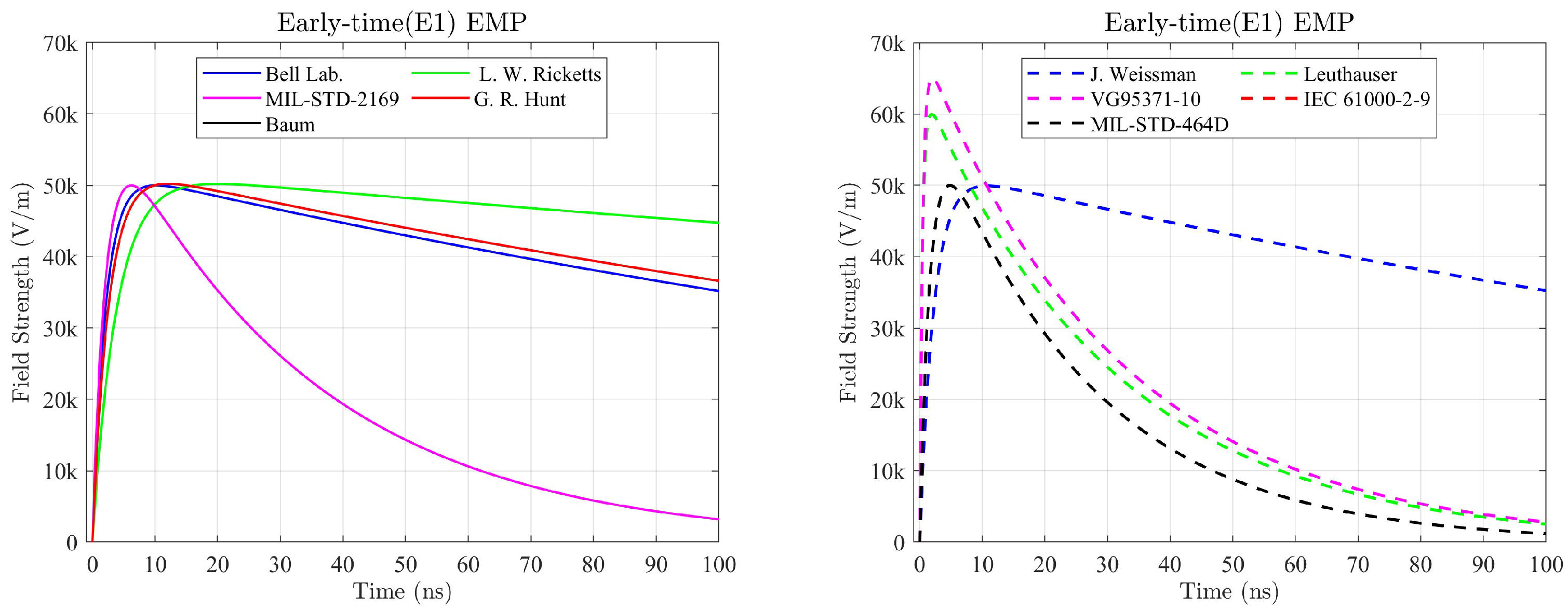
The nuclear EMPs, lightning EMPs, electrostatic discharge, and high-power microwaves all fall into the scope of EMP [18]. Typical EMP waveforms have high peak field intensity, with the electric field intensity reaching 50k V/m or higher, and the intensity increases quickly within an extremely short time. Peak field intensity can be achieved within a few nanoseconds (ns). The frequency spectrum ranges from kilohertz to gigahertz, encompassing low-, medium-, and high-frequency bands. Figure 1 presents the time-domain waveform of a high-altitude EMP (HEMP) radiation field [19]. The early-time EMP (E1), intermediate-time EMP (E2), and late-time EMP (E3) generate three main energies that can cause cumulative damage to electronic equipment. E1 consists of initial energy shock waves induced by gamma rays emitted from a nuclear explosion; such shock waves are sustained for approximately 1 s, resembling extremely intense static electricity. These shock waves can overload the electric circuits of electronic devices and cause short circuits in them within line-of-sight of an explosion. E2 is an extension of E1 and is caused by interactions between high-energy neutrons and air. E2 is similar to a thunderbolt. The duration of E2 may range from several microseconds to several milliseconds (ms). For key infrastructure, the use of surge protection measures can largely reduce possible damage. E3 is a magnetohydrodynamic (MHD) flow generated from the geomagnetic field disturbance resulting from a nuclear explosion. The resultant geomagnetic signal is sustained for longer time from approximately 1 sec to hundreds of seconds. Local magnetic effects build up over entire transmission cable networks and collapse rapidly, thereby overloading equipment connected to electric and communication infrastructure and causing severe damage to electronic equipment connected via long cables.
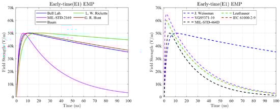
Figure 1.
Environment of early-time EMP [20,21,22,23,24,25,26,27,28,29].
2.1. EMP Waveform
Key EMP standards have been established, such as the International Electrotechnical Commission (IEC) Standards, the Bell Laboratory Standards, and United State Military Standards. Typical EMP waveforms are exhibited through double exponential forms or inverse double exponential forms, as shown in Equations (1) and (2), respectively.
where is the peak electric field intensity, k is the correction constant, are the rise and fall time parameter, respectively.
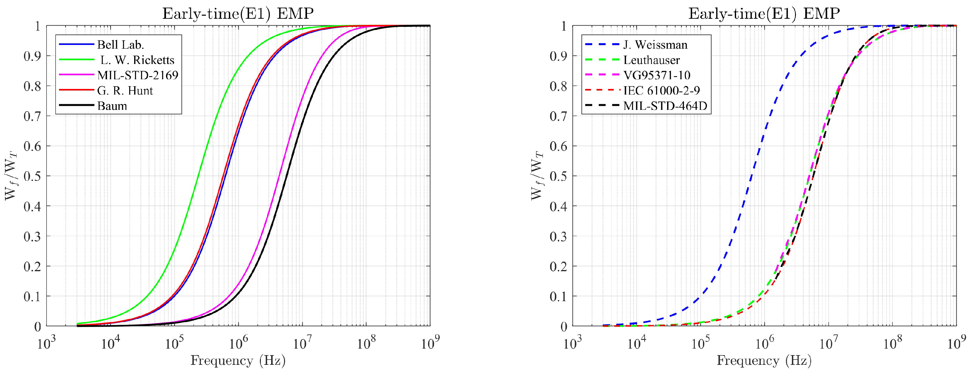
The literature relevant to EMP waveform function parameters was reviewed. The peak electric field value () increases with an increase in explosion energy. Parameters and determine the EMP waveform rise and fall times, respectively. Nanevicz [20] inferred that under the MIL-STD-2169 standard, the E1 waveform function parameters are as follows: (1/s), (1/s), , and = 50,000 (V/m). Table 1 and Figure 1 present comparisons of waveforms and function parameters published in the literature in order of publication date.

Table 1.
Comparison of the characteristics of HEMP waveforms.
E1 has a rapid rise time, short pulse duration, and little variation in trailing time. This study analyzed 10 EMP waveforms and identified that the peak electric field intensity was 50–65 k (V/m). However, the full width at half maximum (FWHM) was considerably different among the 10 waveforms; Ricketts’ waveform had the longest FWHM, followed by Hun’s. VG95371-10 had the shortest FWHM. EMP energy density in the air can be estimated by integrating the electric field function, as shown in Equation (2). The electric field intensity reached its peak of 50–65 k (V/m) within several nanoseconds and dropped quickly over dozens to hundreds of nanoseconds; such drastic change of intensity within a short period of time resulted in considerable variations in inductance, voltage, and current and thereby created intense electromagnetic and electric fields. The highest energy density generated was observed in Ricketts’ waveform, followed by that of Weissman IEC61000-2-9 and MIL-STD-464D had the lowest energy densities.
2.2. EMP Frequency Coverage and Frequency Domain Energy Distribution
The EMP time-domain Equations (1) for double exponential forms and Equations (2) for inverse double exponential forms can be converted into a frequency-domain distribution through Fourier transform, as shown in Equations (3) and (4). According to Parseval’s theorem (or Rayleigh’s energy theorem), when the frequency is higher than 1 kHz under a far-field condition, energy spectrum can be used to describe the relationship between energy density and frequency, as shown in Equation (5). EMP energy flux can be obtained through the integral of Equation (5) in the frequency domain, as shown in Equations (6) and (7). The relationship between cumulative energy and frequency is presented in Figure 2. Energy flux of 100 kHz or lower accounted for approximately 2% of total cumulative energy flux, whereas energy flux of 100 MHz or lower accounted for approximately 98% of total cumulative energy. Therefore, we estimated that the energy of E1 accounted for approximately 96% of the cumulative energy because the E1 energy frequency is between 100 kHz and 100 MHz.
where represent Fourier transform of , angular velocity, and
where represent energy spectrum, = 120, above 1 kHz energy fluence (J/m), from 1 kHz to f energy fluence (J/m).

Figure 2.
Cumulative amount of energy of the early-time EMP of frequency [20,21,22,23,24,25,26,27,28,29].
3. Shielding Effectiveness
The shielding effectiveness (SE) of the outer case or skin of a device depends on the materials used and the pore size of such materials. Sufficiently thick metal materials (e.g., steel and aluminum) can provide adequate mechanical strength and SE. However, pores or grooves on metal materials are common hazards to SE. Thus, most shield designs have focused on reducing the number and size of openings [30]. From the perspective of electromagnetic shielding, an ideal electromagnetic shielding structure should be highly conductive and spherical, with a sufficiently thick metal wall but without seams, pores, personnel exits and entries, windows, or cable inlets and outlets. In practice, the structural appearance of aircrafts or vessels may be affected by system and equipment requirements. For example, the ideal designs of structural appearance and strength based on fluid mechanics principles and task requirements often determine the thickness and materials of structures. In addition, viewing windows, personnel access ways, ventilation, and cable inlets and outlets must be designed to provide air to the personnel and to facilitate transmission of power and signals for electronic equipment. However, these slits, pores, and openings weaken electromagnetic shielding.
3.1. Fundamentals of SE
Electromagnetic shielding involves using shields with satisfactory SE to block or attenuate the electromagnetic energy transmission between the shielded area and the external environment. SE refers to the amount of attenuated electric and magnetic energy after electromagnetic waves pass through a shield. SE is normally expressed in decibels and is related to many variables, including material type, property, thickness, distance, and frequency. SE is generally defined as the logarithmic ratio of the amplitude of the electric field and magnetic field in an unshielded area to the amplitude of the time-harmonic electric field and magnetic field in the same but shielded area at any position, or the logarithmic ratio of the time-averaged power density in an unshielded area to that in the same but shielded area [31], as shown in Equations (9) and (10). Because electric and magnetic fields cannot be considered separately, Equation (9) is mainly applied for low-frequency electric and magnetic fields, and Equation (10) is mainly applied for high-frequency plane waves.
where and are the unshielded and shielded magnetic field intensity (A/m), and are the unshielded and shielded energy (J) of plane wave, respectively.
When an electromagnetic front wave hits the edge of a shield, the electromagnetic wave passes through the shield. The mathematical model of this wave transmission resembles that for the transmission of voltage and currents in a cable. When the incident electromagnetic wave hits the shield [32], a certain amount of incident power in the electric field intensity () and magnetic field intensity () is reflected and then subjected to absorption by the material and n reflections inside the material. The intensity of the electromagnetic wave is attenuated in this process. Mathematically, Equation (11) is used to describe the sum of three types of loss in the SE mechanism, namely absorption attenuation (A), attenuation by reflection (R), and attenuation caused by multiple reflections as a result of the material molecular structure (M) [33]. The relationships of reflection, absorption, and multiple reflections of electromagnetic shielding can also be described using logarithmic functions respectively as follows [34].
3.2. Absorption Attenuation
The skin effect of materials limits the penetration of high-frequency electromagnetic radiation to the surface area of an electrical conductor. The electric field of the plane wave that travels through the material surface decreases exponentially in intensity as the conductor depth increases. Therefore, the skin depth decreases with an increase in frequency or conductivity. When electromagnetic waves penetrate the shielding material, the ohmic losses induce penetration losses through thermal diffusion. Such penetration losses are due to absorption by the shielding material; this type of attenuation occurs as a result of energy absorption. Absorption attenuation is calculated using Equation (13).
where is the skin depth, f is the frequency, and are the vacuum and relative magnetic permeability, is the magnetic permeability, and are the conductivity and resistivity, respectively.
3.3. Reflection Attenuation
An electromagnetic shield reflects waves mainly through the interaction of mobile electrons or holes in the shielding material with the electromagnetic fields of radiation. When an electromagnetic wave travels from the air to the shielding material, reflection occurs in the interface between the two media. Thus, the electromagnetic wave’s intensity along the incident direction is attenuated because of the mismatch between the impedance of free space and the impedance of material . Reflection attenuation is calculated using Equation (14).
3.4. Multiple Reflection Attenuation
In addition to reflection and absorption, shielding involves a mechanism of multiple reflections between surfaces or interfaces in a shield. Multiple reflections require the presence of large surface areas or interfacial areas in a shield. Multiple reflection–induced losses occur due to a second reflection or multiple reflections inside the shield material. When an electromagnetic wave passes through a shielding material, multiple interfacial reflections occur between the environment and the material. Multiple reflection attenuation can be calculated using Equation (15). If the material thickness (t) is substantially greater than the skin depth (), the effect of multiple reflections can be ignored. However, if the material thickness (t) is substantially lower than the skin depth (), the attenuation becomes negative and the SE declines. Thus, when the distance between the reflection surfaces or interfaces is substantially greater than the skin depth, the loss resulting from multiple reflections is negligible.
Absorption and reflection attenuations are the primary means through which materials shield electromagnetic waves. At low frequencies, because the material skin depth is high, and the absorption attenuation is low, SE is mainly dependent on reflection attenuation. With higher frequencies, the electromagnetic wave skin depth decreases, and the absorption attenuation increases. When the frequency increases to a point where the absorption attenuation is sufficiently large, the SE is determined by absorption attenuation. However, the fact that reflection attenuation is largely related to environmental impedance and material impedance and that the effect of electric waves is greater than that of the magnetic waves on SE at low frequencies makes electromagnetic shielding more difficult in low-frequency conditions compared with high-frequency ones.
3.5. Protective Benefits of Shielding Attenuation
In 2019, the National Coordinating Center for Communications (NCC) developed Electromagnetic Pulse (EMP) Protection and Resilience Guidelines for Critical Infrastructure and Equipment and defined four EMP protection levels. In the guidelines, the Level 3 protection refers to high-frequency EMP shielding of at least 30 dB provided to “organizations, facilities, and systems that cannot tolerate more than a few minutes of mission outage due to EMP”. The EMPs of a high-altitude nuclear detonation with an electric field intensity of 50 k V/m generates energy density in the air of approximately 11.4 J/cm. With a 30 dB attenuation provided by the shield, the energy density can be attenuated by 1000 times to 0.0114 J/cm. The EMP field intensity is attenuated by at least 97%. In the Level 4 protection guidelines, at least 80 dB protection against high-frequency EMP is provided to military equipment, such as command, control, communications, computer, and intelligence systems. With this level of protection, EMP field intensity is attenuated by at least 99.99%.
4. Experimental Setup and Results
4.1. Experimental Setup
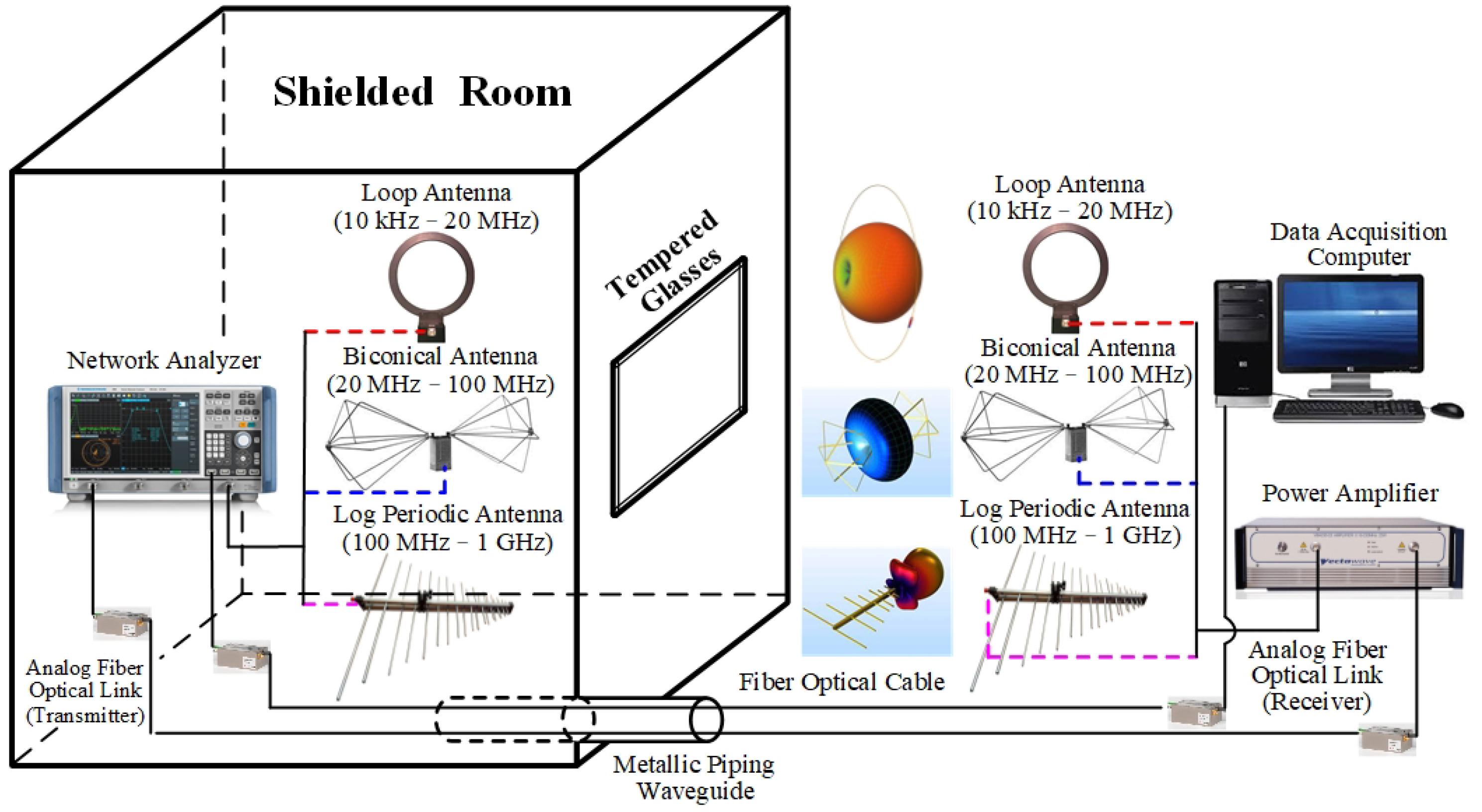
MIL-STD-188-125 [35] SE measurement involves stepped frequency measurement to minimize the area and points to be tested. The transmitting antennas are placed at the center of each test area (or test point), and the receiving antennas are placed in the center of the test area (or test point) on the opposite side of the shield. The distance between the transmitting and receiving antennas is maintained at 3.05 m, as shown in Figure 3. The measurement equipment is detailed in Table 2, and the measurement data are recorded for each frequency step. The measurement range of the magnetic field SE is between 10 kHz and 20 MHz. The SE measurement range for the resonant range/plane electromagnetic wave is between 20 MHz and 1 GHz. In terms of sampling frequency, measurements were conducted at 20 points from 10 kHz to 100 kHz, 20 points from 100 kHz to 1 MHz, 40 points from 1 MHz to 10 MHz, 150 points from 10 MHz to 100 MHz, and 150 points from 100 MHz to 1 GHz.
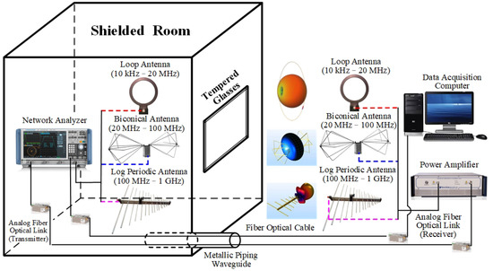
Figure 3.
Shielding effectiveness instrumentation system.
Table 2.
Shielding effectiveness test equipments characteristics.
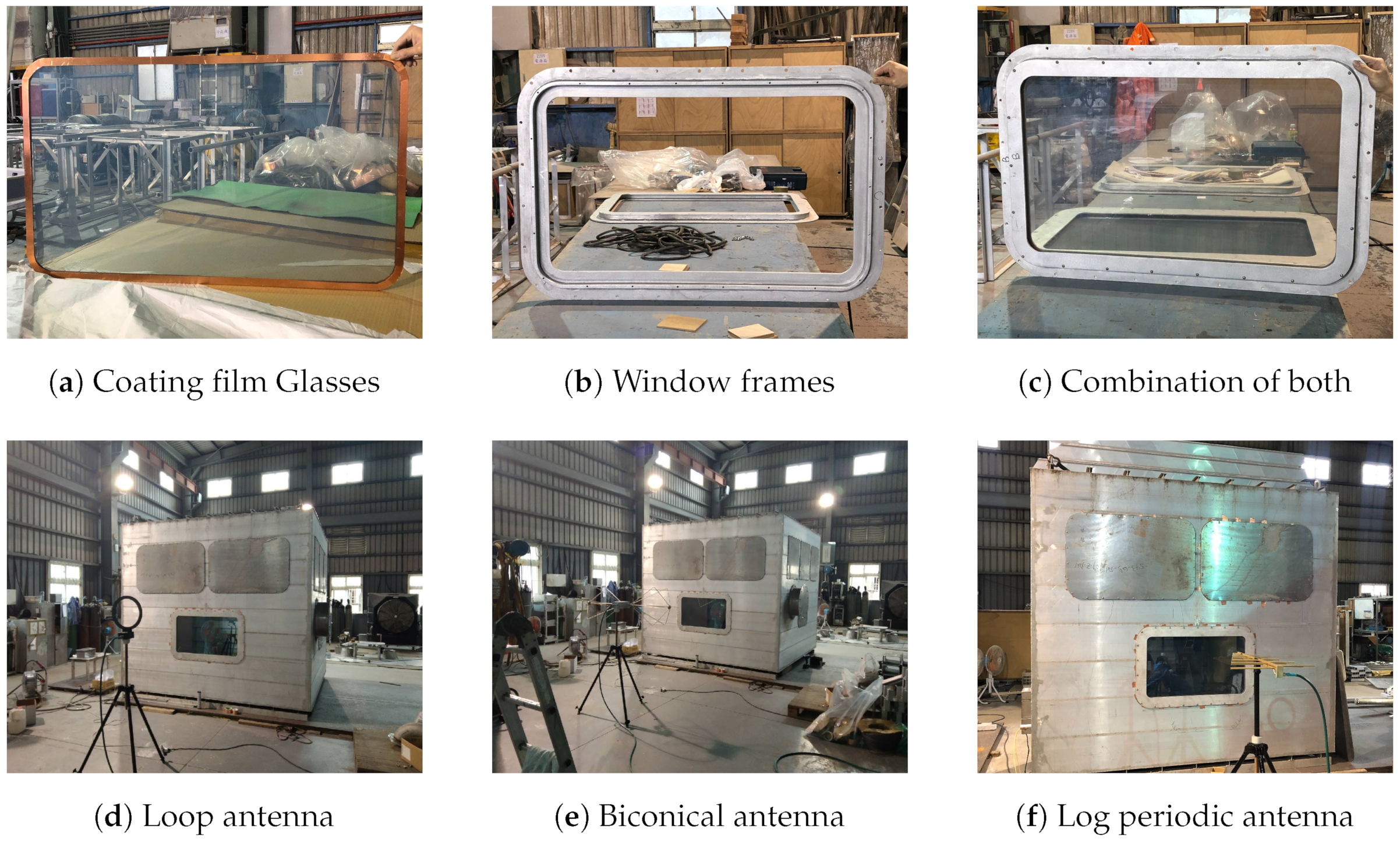
The frequency range of antenna reception and transmission must satisfy dynamic bandwidth requirements. Corresponding antennas were used for different test bandwidths. A network analyzer and a power amplifier were used to generate and amplify signals to the transmitting antennas placed outside a shielded room, which were a loop antenna (10 kHz∼20 MHz), a biconical antenna (20 MHz∼100 MHz), and a log periodic antenna (100 MHz∼1 GHz). After signals were attenuated through the shielding material, the corresponding antennas inside the shielded room received the signals. Subsequently, the SE can be calculated by comparing the signal attenuation levels inside and outside the shielded room.
4.2. Far Field Regions of an Antenna
The peripheral radiation field of an antenna consists of three fields (from near to far: the reactive near field, near field, and far field).
- Reactive near field: This field is a near-field region close to the antenna aperture in the antenna radiation field. The transformation between the electric and magnetic fields is similar to the transformation between the electric and magnetic fields in a transformer and manifests as reactive energy storage. The field usually covers the area between the antenna aperture surface to /2 away from the antenna. The boundary condition of this field is as follows:
- Near field: This field is also called the Fresnel zone; it is located between the reactive near field and the far field. The electromagnetic field is at a distance from an antenna and enters the air in the form of an electromagnetic wave. The boundaries of the far field and the near field are defined by the distance between transmitting and receiving antennas. In this region, the reactive field effect is substantially lower than that of the radiation field. The radiation pattern and angle change with antenna distance. The boundary of the region is as follows:
- Far field: This field is also called the Fraunhofer zone; its location ranges from outside the near field to infinity. The reactive field no longer exerts any effect in this field, and the radiation pattern is unrelated to distance change. The radiation field transmitted from any point of the antenna must have a phase difference of lower than /8 when it reaches the observation point. The far field condition is as follows:
The coated glass SE was measured in free space with a frequency range between 10 kHz and 1 GHz. A network analyzer was used to measure the transmission coefficients of the loop antenna (10 kHz∼20 MHz), the biconical antenna (20∼100 MHz), and the log periodic antenna (100 MHz∼1 GHz). For far-field measurements, the transmitting and receiving antennas must be kept at a distance of at least 0.0124, 1.1452, and 2.9075 m for the loop antennas, the biconical antennas, and the log periodic antennas, respectively, as shown in Table 3. In this study, the distance between each pair of transmitting and receiving antennas was maintained at 3.05 m to satisfy said distance requirement for far-field radiation measurements.
Table 3.
Minimum distance for far field.
4.3. Shielding Effectiveness of Shielded Room
The design of an experimental site for measuring electromagnetic SE has three requirements. The first requirement is eliminating the potential effects of external electromagnetic waves on the device under test (DUT). If the DUT lacks an electromagnetic shielding case to protect it from such waves, they could potentially affect the DUT through the inlets and outlets of cables and ventilation systems. The second requirement is keeping certain radio frequency signals within the outer case to reduce the possibility of radio frequency signals affecting the DUT. The third requirement is a combination of the previous two requirements. Effective electromagnetic shields can isolate radio frequency energies inside and outside the outer case.
Given that a completely closed aluminum alloy–based electromagnetically shielded room was used for the experiment, the study focused on absorption attenuation without considering reflection attenuation. Under the conditions of aluminum magnetic permeability () of (H/cm), resistivity () of , conductivity () of (S/cm), and frequency of 100 kHz, Equation (12) can be used to derive the electromagnetic skin depth () of aluminum alloy as 0.846 mm. When this value is substituted into Equation (13), a shielding attenuation of 41.0729 dB is obtained for a 4 mm aluminum alloy plate. However, in practice, personnel exits and entries as well as cable inlets and outlets are required for a shielded room, which inevitably reduces the electromagnetic SE of the room.
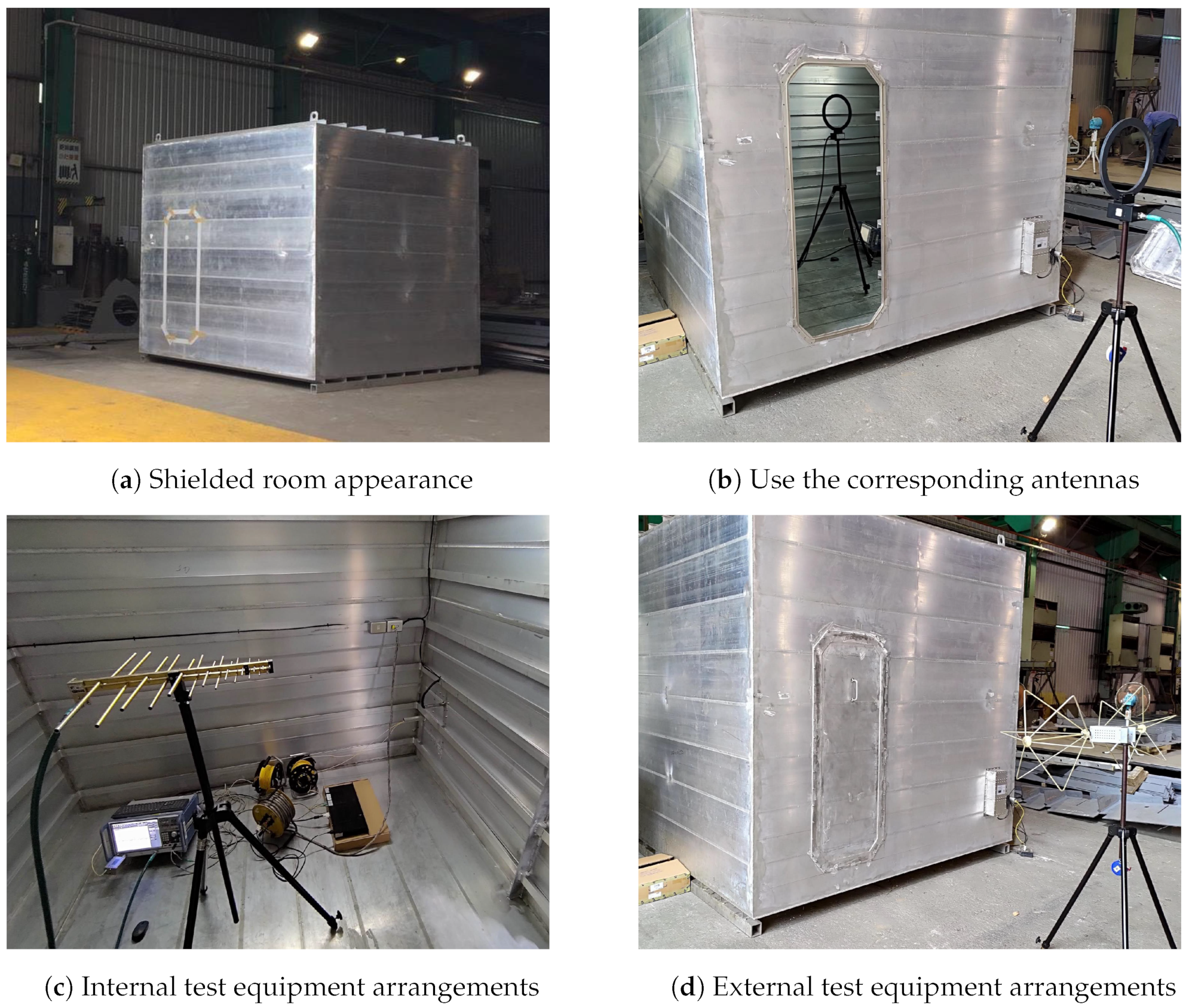
To prevent potential interferences from electric or magnetic field, which may undermine the accuracy of the experimental SE measurements of the conductive coated glass, the present study used 6082-T6 aluminum alloy with a plate thickness of 4 mm to build a hexahedron closed or nearly closed electromagnetically shielded room with dimensions of 3000 × 3000 × 3000 mm. Radio frequency signal–receiving antennas were placed in the shielded room, and radiofrequency signal–transmitting antennas were placed outside the room, as indicated in Figure 4. The transmitting antennas transmitted radio frequency signals within the operating frequency range of 10 kHz∼1 GHz. The receiving antennas recorded all received signals. All transmitted signal energy not received was determined to be the amount of attenuation by material shielding.
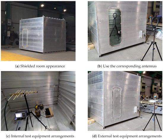
Figure 4.
Shielded room configurations and shielding effectiveness measurements.
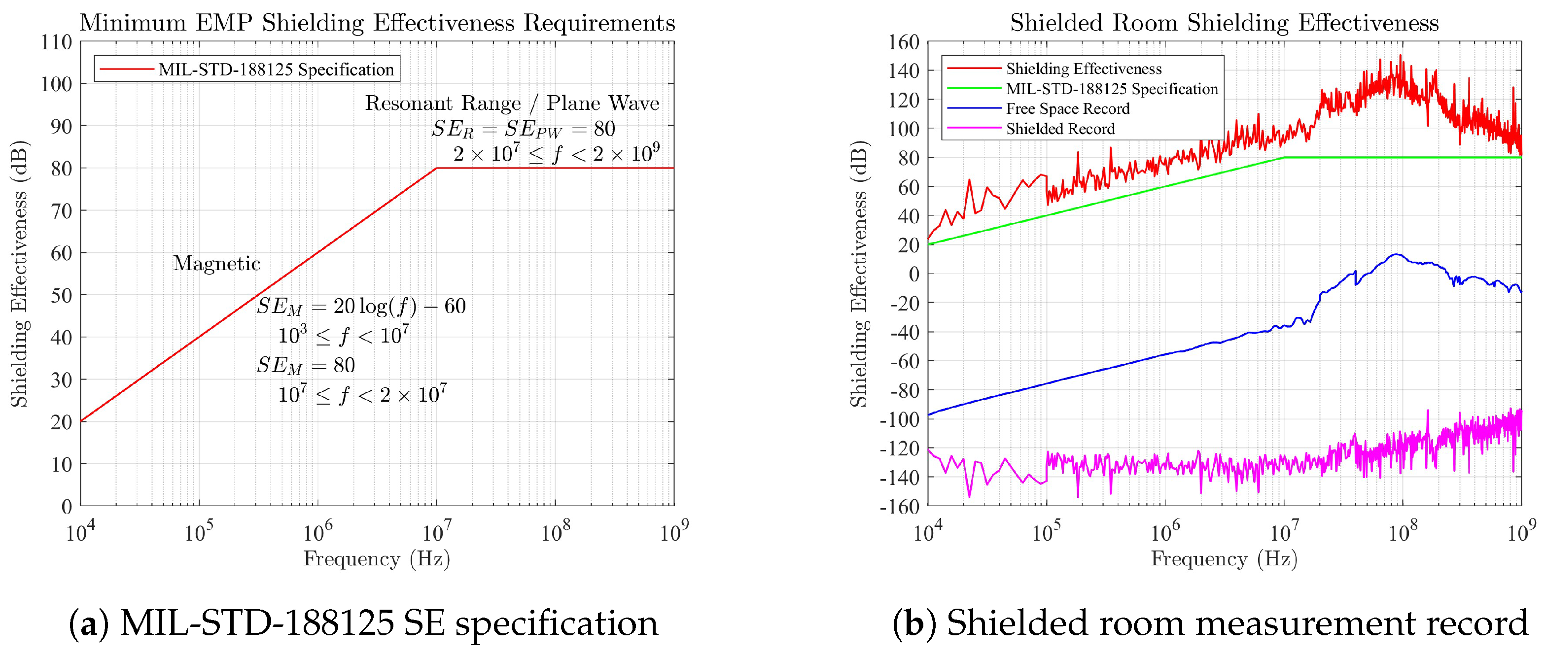
First, the SE of the shielded room against the magnetic and electric fields was measured to increase the accuracy and reliability of the experiment. The measurement results revealed that the shielded room’s SE against the magnetic field was 10 dB higher than the (dB) electromagnetic shielding requirement at the 10 kHz∼10 MHz frequency. For the electric field, the SE was all greater than 80 dB at a frequency range between 10 MHz and 1 GHz. The results are presented in Figure 5. The shielded room satisfied the shielding specification of MIL-STD-188-125, and thus it was applicable for electromagnetic SE measurement experiments.
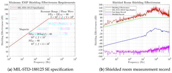
Figure 5.
Shielded room shielding effectiveness of experiments.
4.4. Resistivity and Transmittance of Coating Tempered Glasses Measurements
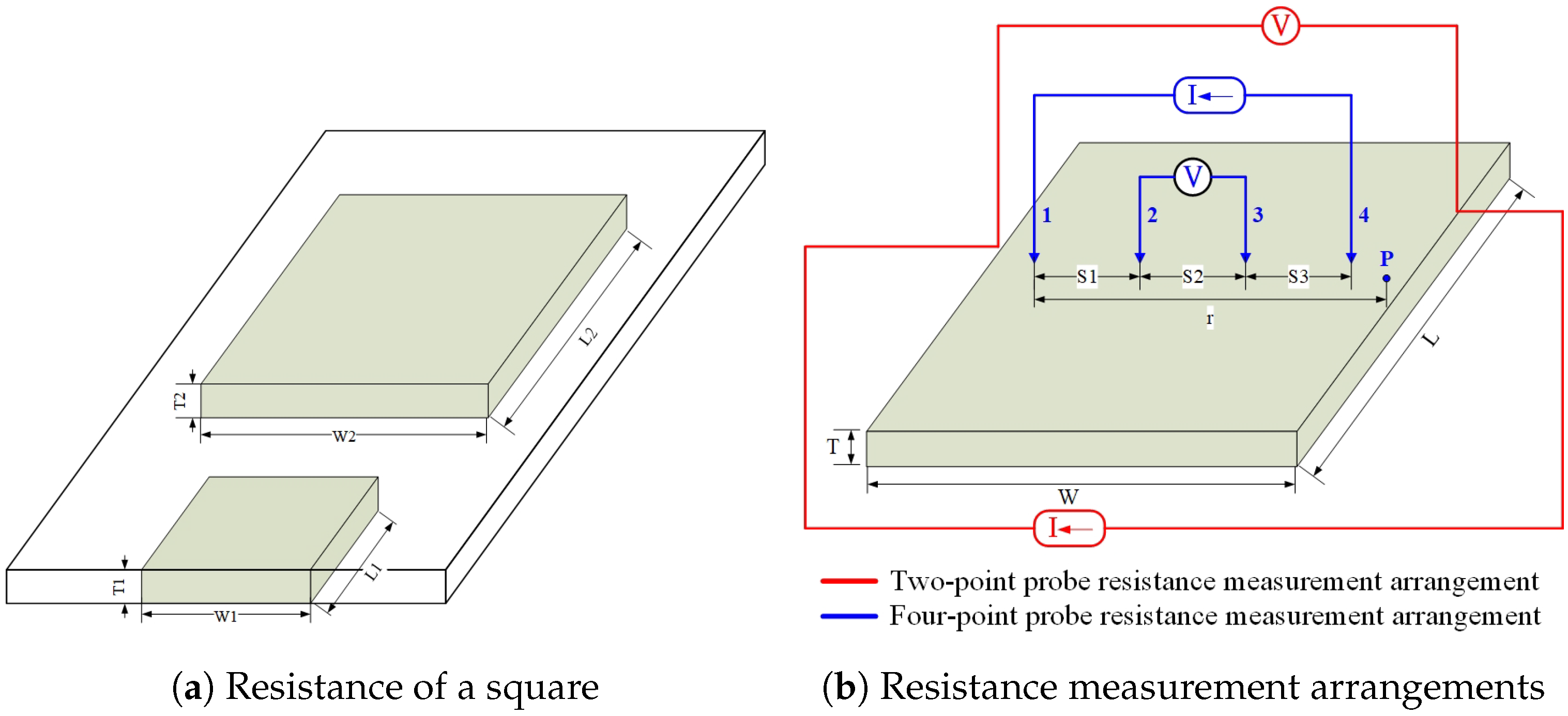
The present study used a four-point probe method, which involves passing a current through two probes and measuring voltage with the other two probes, as shown in Figure 6. This method is normally used to measure semiconductor resistivity. A direct and absolute measurement can be obtained without additional instruments. The four-point probe is composed of four thin metal probes aligned in a row. During thin-film resistivity measurement, the current passes through the two outer probes, and the voltage drop passes through the inner probes. The entire measurement process can be completed within a thin film layer.
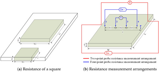
Figure 6.
Two-point probe and four-point probe resistance measurement arrangements.
The electric physical quantity measured on the thin film is called sheet resistance (Rs). The unit is ohms per square (). Sheet resistance is the resistance flowing from one square region to an opposite square region. When L1 is W1 and L2 is W2, the same sheet resistance exists on any square size regions, as shown in Figure 6a. The four-point probe was used to measure the thin film sheet resistance. The relationships between the voltage, current, and resistance conformed to Ohm’s law. The current (I) enters from Probe 1 and exits from Probe 4, as shown in Figure 6b. The relationships of the electric field (E) with the current density (J), voltage (V), resistivity (), and electrode distance (r) are expressed using Equations (16)–(23) [36]:
where and are the distances from Point P to Probe 1 and to Probe 4, respectively. A negative sign indicates that the current leaves the probe. The reference potential is as follows:
The spacings between probes are , , and . In accordance with the potentials of Probe 2 () and Probe 3 (), the potential difference can be measured as follows:
For a regular four-point probe, the spacing between probes is identical: . The resistivity () is calculated using Equation (22). The thickness of the conductive thin film can be calculated by measuring the film resistance with the four-point probe and then substituting the resistance value into Equation (23).
Resistivity () is crucial to thin film conductivity. The resistivity is determined by the densities of free electron and hole n and p as well as the mobilities of electrons and holes and . The relationship between resistivity and said densities and mobilities can be expressed in Equation (24). Free electrons and holes can carry electric charge and can be collectively referred to as carriers. A current is caused by the movement of negatively charged free electrons and positively charged holes. Resistivity is closely related to carrier density, electron charge, and carrier mobility.
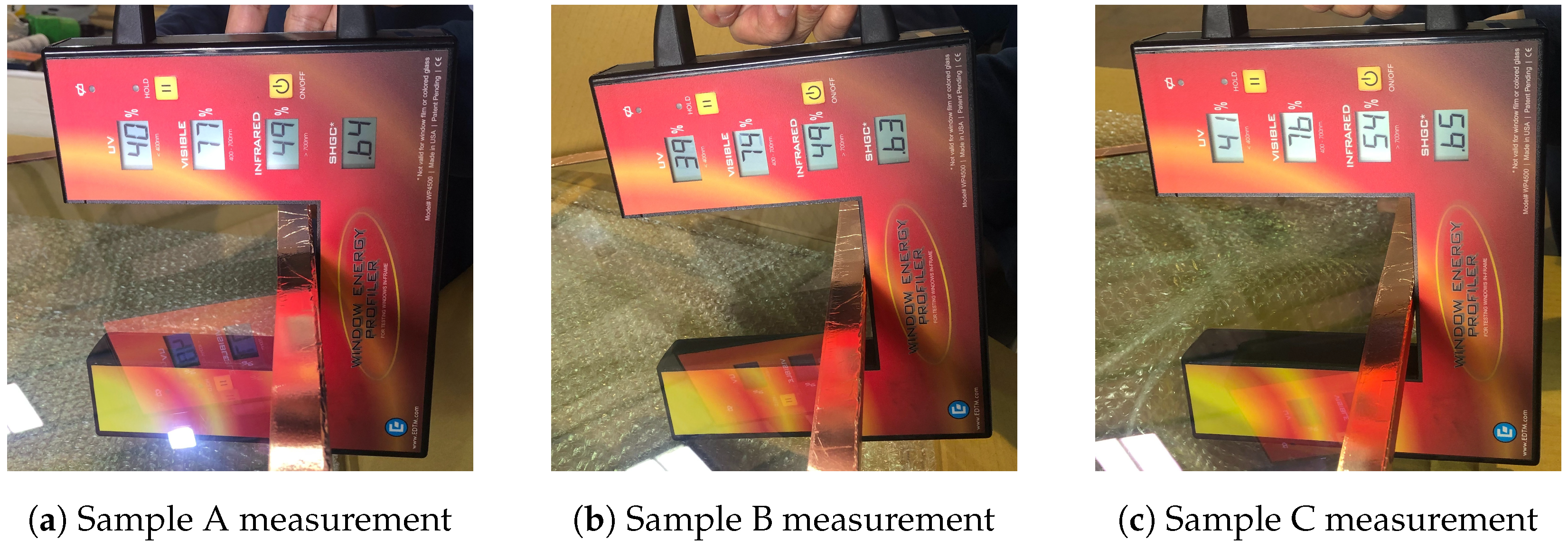
In general, an increase in carrier concentration and film thickness increases conductivity but reduces transmittance. Thus, an optimal combination of conductivity and transmittance should be determined. This study doped metal oxide additives, such as In2O3, SnO2, Ta2O5, NbO, SiO2, TiO2, and Al2O3 to different conductor types at different mixture ratios and coated the resultant substance separately onto three 1000 mm×600 mm× 10 mm glass targets. According to the measurement results, the transmittance of the three coated glass targets reached 74% to 77%, as shown in Figure 7. The film resistivity values were 6.8, 6.4, and 6.5 , as shown in Figure 8. The parameter characteristics are shown in Table 4. The purpose of coating aforementioned conductive metal oxide additives to glass is to form conductive continuity between conductive oxides on the glass surface and the metal structures around the glass. When conductive particles make contact with one another, electron continuity is formed. As the external electromagnetic field reaches the outer part of the conductive particles, electromagnetic waves hit the free electrons on the conductive particles, and these free electrons form an electromagnetic field opposite to that of the external electromagnetic field. The internal and external electromagnetic fields offset each other, resulting in the attenuation of the electromagnetic interference.

Figure 7.
Coating tempered glasses visible light transmittance measurements scenes.
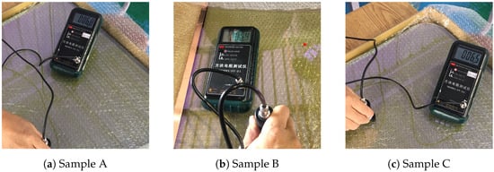
Figure 8.
Coating tempered glasses sheet resistance measurements scenes.
Table 4.
Coating tempered glasses parameter characteristics.
4.5. Shielding Effectiveness of Coating Tempered Glasses
For window glass coated with a conductive thin film to be integrated with a metal structure, conductive continuity is required between the conductive medium and the shielding metal structure. Therefore, the seam between the window frame and metal structure should minimized to reduce electromagnetic leakage. For example, conductive rubber filled with conductive particles can be used to inhibit electromagnetic leakage. The researchers of this study installed the three glass samples in a shielded room to measure electromagnetic shielding, as shown in Figure 9.

Figure 9.
Coating tempered glasses shielding effectiveness measurements scenes.
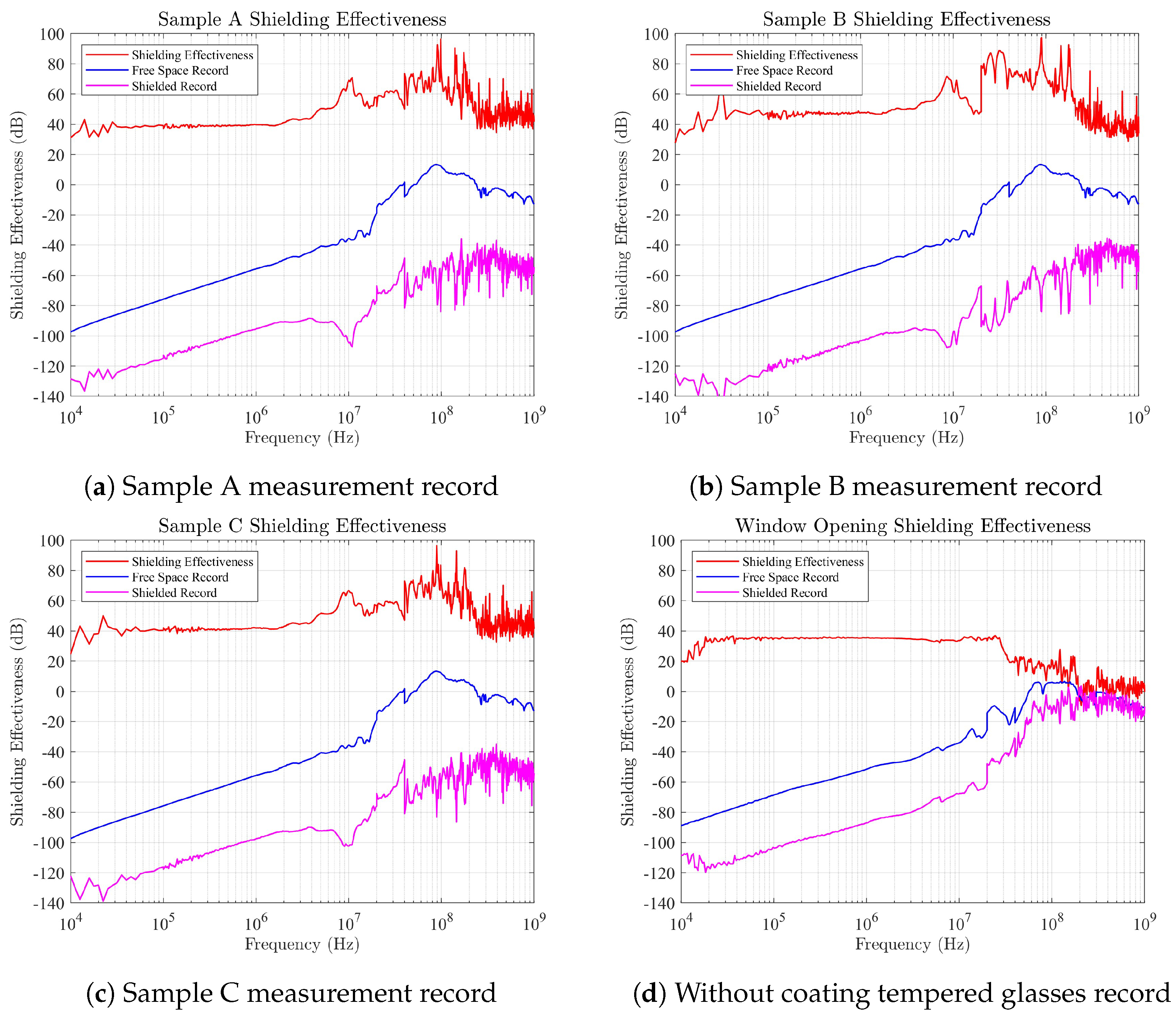
The measurement results revealed that in a low-frequency magnetic field (10 kHz∼100 MHz), Sample B exhibited superior performance with shielding attenuation of at least 45.1 dB. Sample A had inferior performance, with an average shielding attenuation of 37 dB. Under high-frequency plane waves (100 MHz∼1 GHz), the shielding performance declined gradually. At 100∼300 MHz, the decrease in SE was the most notable, with the minimum shielding attenuation observed at 32 dB. At a frequency band between 10 kHz and 100 MHz, the SE reached a minimum of 45.1 dB and a maximum of over 80 dB. At the frequency band of 10 kHz, where shielding is challenging, the SE attains 31.1 dB. To empirically substantiate the electromagnetic wave shielding efficacy of the three conductive film glass samples featured, remove the conductive film glass from the shielding enclosure, exposing apertures equivalent to a glass dimension of 1000 mm by 600 mm. These findings reveal that the shielding enclosure demonstrates negligible electromagnetic wave shielding effectiveness in the absence of conductive film glass, particularly within the high-frequency domain from 100 MHz to 1 GHz. Here, the transmission loss of electromagnetic wave energy closely mirrors that in free space, with the electromagnetic waves nearly thoroughly permeating the interior of the shielding enclosure. The shielding attenuation decreased gradually; however, the SE remained at 32 dB or higher, as indicated in Figure 10.
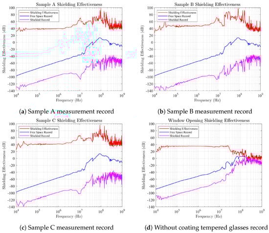
Figure 10.
Coating tempered glasses shielding effectiveness of experiments.
The experimental results revealed that the conductive-coated glass targets had favorable electromagnetic SE and satisfied the NCC Level 3 requirement of ≥30 dB shielding protection. The glass attenuated energy density by more than 1000 times, which is equivalent to shielding over 97% of the electromagnetic wave energy. The glass targets have practical value for installation as high-transmittance conductive glass materials on the windows of automobiles, vessels, and aircraft to protect against EMP.
5. Conclusions
This study built a metal shielded room that satisfied MIL-STD-188-125 requirements and substantially increased the precision of electromagnetic SE measurements in its experiments on glass samples with conductive coating.
- The conductive-coated glass samples had ∼ (S/cm) conductivity (); the resistivity () was reduced down to ; and the light transmittance was 74% or higher. At a frequency band of 20 kHz∼100 MHz, the glass samples had the minimum SE of 40 dB and the maximum SE of over 80 dB. At a frequency band of 10 kHz, where shielding is challenging, the SE remained at 31.1 dB or higher. At a frequency band of 100 MHz∼1 GHz, the shielding attenuation decreased gradually; however, SE of at least 32 dB was achieved. These glass materials have practical value as high-transmittance conducive materials for windows of automobiles, vessels, and aircrafts to protect against EMP.
- The electromagnetic SE of conductive-coated glass materials increases with an increase in conductive film thickness. However, the transmittance decreases as film thickness increases. Research is thus warranted to find an optimal combination of the thin film thickness and transmittance.
- Conductive-coated glass and its surrounding metal structure are heterogenous materials. A conductive medium is required to facilitate conductive continuity between the glass and metal structure to achieve effective electromagnetic shielding. The integrative design of a piece of conductive-coated glass, a glass framework, and its surrounding metal structure as well as the selection of materials merit further attention.
- In this study, experiments were conducted to measure the electromagnetic SE of conductive-coated glass materials. Future studies may incorporate numerical simulation analysis into the discussion to facilitate comprehensive and in-depth explorations.
Author Contributions
Conceptualization, S.-F.T., C.-M.C. and S.-Y.L.; methodology, C.-M.C. and Y.-H.C.; software, S.-Y.L. and S.-F.T.; resource, C.-M.C., S.-Y.L. and S.-F.T.; supervision, S.-D.C. and S.-F.T.; writing—original draft preparation, Y.-H.C. and C.-M.C.; writing—review and editing, S.-F.T. and S.-D.C. All authors have read and agreed to the published version of the manuscript.
Funding
This work was partially supported by NSTC of Taiwan R.O.C. through NSTC 112-2221-E-002 -141 -MY2 and NSTC 112-2222-E-019-001.
Institutional Review Board Statement
Not applicable.
Informed Consent Statement
Not applicable.
Data Availability Statement
Data are contained within the article.
Conflicts of Interest
The authors declare that there are no conflict of interest regarding the publication of this paper.
References
- Hao, R.; Zhang, X.; Gao, H.; Wu, H.; Cheng, J.; Li, G.P. A novel high-altitude electromagnetic pulse (HEMP) protection circuit for RF applications. Microelectron. J. 2019, 84, 1–8. [Google Scholar] [CrossRef]
- Hamamah, F.; Ahmad, W.F.H.W.; Gomes, C.; Isa, M.M.; Homam, M.J. High power microwave devices: Development since 1880. In Proceedings of the 2017 IEEE Asia Pacific Microwave Conference (APMC), Kuala Lumpur, Malaysia, 13–16 November 2017; pp. 825–828. [Google Scholar] [CrossRef]
- Kim, K.; Min, K.R.; Park, Y.J. A Pilot Experiment to Develop a Lightweight Non-Nuclear EMP Shelter Applying Civil-Military Cooperation in a Sustainability Policy. Sustainability 2020, 12, 10669. [Google Scholar] [CrossRef]
- Taflove, A.; Oskooi, A.; Johnson, S.G. Advances in FDTD Computational Electrodynamics: Photonics and Nanotechnology; Artech House: London, UK, 2013. [Google Scholar]
- Wang, C.; Murugadoss, V.; Kong, J.; He, Z.; Mai, X.; Shao, Q.; Chen, Y.; Guo, L.; Liu, C.; Angaiah, S.; et al. Overview of carbon nanostructures and nanocomposites for electromagnetic wave shielding. Carbon 2018, 140, 696–733. [Google Scholar] [CrossRef]
- Yang, C.; Liu, P.G.; Huang, X.J. A Novel Method of Energy Selective Surface for Adaptive HPM/EMP Protection. IEEE Antennas Wirel. Propag. Lett. 2013, 12, 112–115. [Google Scholar] [CrossRef]
- Lu, Z.H.; Liu, P.G.; Huang, X.J. A Novel Three-Dimensional Frequency Selective Structure. IEEE Antennas Wirel. Propag. Lett. 2012, 11, 588–591. [Google Scholar] [CrossRef]
- Holloway, C.; Hill, D.; Ladbury, J.; Koepke, G.; Garzia, R. Shielding effectiveness measurements of materials using nested reverberation chambers. IEEE Trans. Electromagn. Compat. 2003, 45, 350–356. [Google Scholar] [CrossRef]
- Ming, W.; Ming, C. Modeling for electromagnetic pulse shielding effectiveness in time domain. In Proceedings of the 2015 7th Asia-Pacific Conference on Environmental Electromagnetics (CEEM), Hangzhou, China, 4–7 November 2015; pp. 176–179. [Google Scholar] [CrossRef]
- Yan, Z.; Qin, F.; Cai, J.; Zhong, S.; Lin, J. Shielding Performance of Materials Under the Excitation of High-Intensity Transient Electromagnetic Pulse. IEEE Access 2021, 9, 49697–49704. [Google Scholar] [CrossRef]
- Lee, H.S.; Choe, H.B.; Baek, I.Y.; Singh, J.K.; Ismail, M.A. Study on the Shielding Effectiveness of an Arc Thermal Metal Spraying Method against an Electromagnetic Pulse. Materials 2017, 10, 1155. [Google Scholar] [CrossRef] [PubMed]
- Phan, D.T.; Jung, C.W. High Optical Transparent and Shielding Effectiveness Using Metal Mesh and Saltwater for Transparent EMI Shielding Applications. In Proceedings of the 2020 IEEE International Conference on Consumer Electronics-Asia (ICCE-Asia), Seoul, Republic of Korea, 1–3 November 2020; pp. 1–4. [Google Scholar] [CrossRef]
- Greco, S.; Sarto, M.S.; Tamburrano, A. Shielding performances of ITO transparent windows: Theoretical and experimental characterization. In Proceedings of the 2008 International Symposium on Electromagnetic Compatibility—EMC Europe, Hamburg, Germany, 8–12 September 2008; pp. 1–6. [Google Scholar] [CrossRef]
- Grunthaner, F.J.; Grunthaner, P.J.; Maserjian, J. Radiation-Induced Defects in SiO2 as Determined with XPS. IEEE Trans. Nucl. Sci. 1982, 29, 1462–1466. [Google Scholar] [CrossRef]
- Qin, M.J.; Kuo, E.Y.; Whittle, K.R.; Middleburgh, S.C.; Robinson, M.; Marks, N.A.; Lumpkin, G.R. Density and structural effects in the radiation tolerance of TiO2 polymorphs. J. Phys. Condens. Matter 2013, 25, 355402. [Google Scholar] [CrossRef] [PubMed]
- Shablonin, E.; Popov, A.; Prieditis, G.; Vasil’chenko, E.; Lushchik, A. Thermal annealing and transformation of dimer F centers in neutron-irradiated Al2O3 single crystals. J. Nucl. Mater. 2021, 543, 152600. [Google Scholar] [CrossRef]
- Kajal, R.; Kataria, B.; Asokan, K.; Mohan, D. Effects of gamma radiation on structural, optical, and electrical properties of SnO2 thin films. Appl. Surf. Sci. Adv. 2023, 15, 100406. [Google Scholar] [CrossRef]
- Nguyen, L. Conductive Concrete Structures for EMP Protection of Critical Infrastructure Facilities. IEEE Lett. Electromagn. Compat. Pract. Appl. 2019, 1, 26–33. [Google Scholar] [CrossRef]
- Morrow-Jones, J. Nominal High-Altitude Electromagnetic Pulse (HEMP) Waveforms; Technical Report AD1067769; Defense Technical Information Center: Washington, DC, USA, 2019. [Google Scholar]
- Nanevicz, J.; Vance, E.; Radasky, W.; Uman, M.; Soper, G.; Ma Pierre, J. EMP susceptibility insights from aircraft exposure to lightning. IEEE Trans. Electromagn. Compat. 1988, 30, 463–472. [Google Scholar] [CrossRef]
- Bell Telephone Laboratories, L.T.D. EMP Engineering and Design Principles; Bell Laboratories: Hoboken, NJ, USA, 1975. [Google Scholar]
- Ricketts, L.W.; Bridges, J.E.; Miletta, J. EMP Radiation and Protective Techniques; Wiley: New York, NY, USA, 1976. [Google Scholar]
- Hunt, G.; Fisher, W. EMP ship trial, planning, execution and result. In Proceedings of the Seventh International Conference on Electromagnetic Compatibility, York, UK, 28–31 August 1990; pp. 308–317. [Google Scholar]
- Baum, C. From the electromagnetic pulse to high-power electromagnetics. Proc. IEEE 1992, 80, 789–817. [Google Scholar] [CrossRef]
- Weissman, J. Composite and exoatmospheric EMP influence on naval vessels. In Proceedings of the 1992 Regional Symposium on Electromagnetic Compatibility, Tel-Aviv, Israel, 2–5 November 1992; pp. 5.2.1/1–5.2.1/8. [Google Scholar] [CrossRef]
- Leuthäuser, K.D. A Complete EMP Environment Generated by High-Altitude Nuclear Bursts—Data and Standardization; Fraunhofer-Institut für Naturwissenschaftlich-Technische Trendanalysen INT: Euskirchen, Germany, 1994. [Google Scholar]
- Electromagnetic Compatibility (EMC) Including Electromagnetic Pulse (EMP) and Lightning Protection—Fundamentals—Part 10: Threat Levels for NEMP and Lightning; Technical Report VG 95371-10:1995; Bundesamt für Ausrüstung, Informationstechnik und Nutzung der Bundeswehr: Koblenz, Germany, 1995.
- Electromagnetic Compatibility (EMC)—Part 2: Environment—Section 9: Description of HEMP Environment—Radiated Disturbance; Basic EMC Publication; Technical Report IEC 61000-2-9:1996; International Electrotechnical Commission: Geneve, Switzerland, 1996.
- Electromagnetic Environmental Effects Requirements for Systems; Technical Report MIL-STD-464D; Department of Defense: Washington, DC, USA, 2020.
- Evans, R.W. Design Guidelines for Shielding Effectiveness, Current Carrying Capability, and the Enhancement of Conductivity of Composite Materials. In Proceedings of the NASA/CR-4784; NASA Contractor Report 4784; NASA: Washington, DC, USA, 1997. [Google Scholar]
- Klinkenbusch, L. On the shielding effectiveness of enclosures. IEEE Trans. Electromagn. Compat. 2005, 47, 589–601. [Google Scholar] [CrossRef]
- Iqbal, A.; Kwon, J.; Kim, M.K.; Koo, C. MXenes for electromagnetic interference shielding: Experimental and theoretical perspectives. Mater. Today Adv. 2021, 9, 100124. [Google Scholar] [CrossRef]
- Afilipoaei, C.; Teodorescu-Draghicescu, H. A Review over Electromagnetic Shielding Effectiveness of Composite Materials. Proceedings 2020, 63, 23. [Google Scholar] [CrossRef]
- Chung, D. Materials for electromagnetic interference shielding. Mater. Chem. Phys. 2020, 255, 123587. [Google Scholar] [CrossRef]
- High-Altitude Electromagnetic Pulse (HEMP) Protection for Ground-Based C4I Facilities Performing Critical, Time-Urgent Missions; Technical Report MIL-STD-188/125-1; Department of Defense: Washington, DC, USA, 1998.
- Schroder, D.K. Contact Resistance and Schottky Barriers. In Semiconductor Material and Device Characterization; John Wiley & Sons, Ltd.: Hoboken, NJ, USA, 2005; Chapter 3; pp. 127–184. [Google Scholar] [CrossRef]

Disclaimer/Publisher’s Note: The statements, opinions and data contained in all publications are solely those of the individual author(s) and contributor(s) and not of MDPI and/or the editor(s). MDPI and/or the editor(s) disclaim responsibility for any injury to people or property resulting from any ideas, methods, instructions or products referred to in the content. |
© 2023 by the authors. Licensee MDPI, Basel, Switzerland. This article is an open access article distributed under the terms and conditions of the Creative Commons Attribution (CC BY) license (https://creativecommons.org/licenses/by/4.0/).