
Field Ion Microscopy of Tungsten Nano-Tips Coated with Thin Layer of Epoxy Resin

 ,
,  ,
,  ,
,  , ,
, , 
Abstract
:1. Introduction
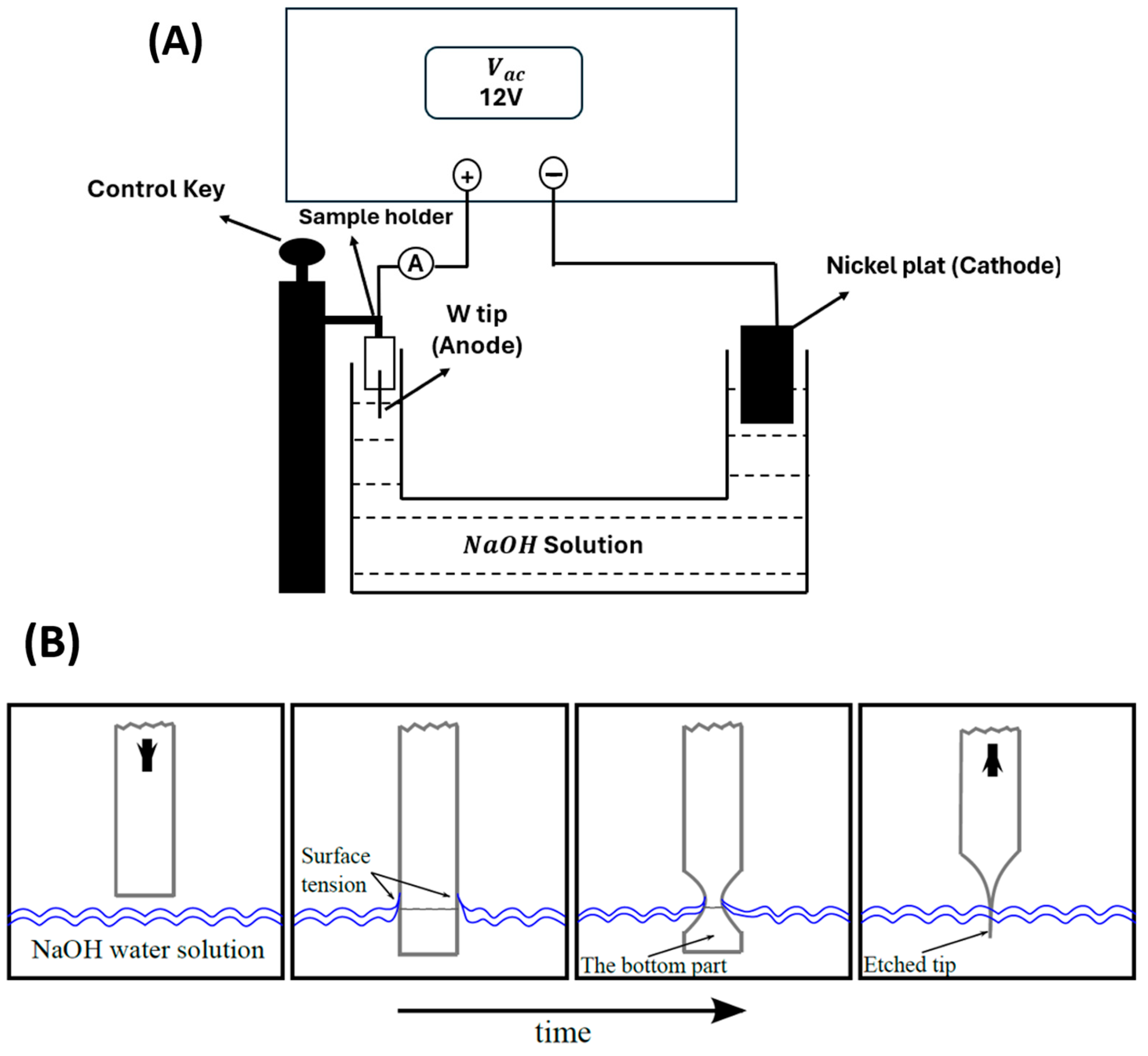
2. Sample Preparation
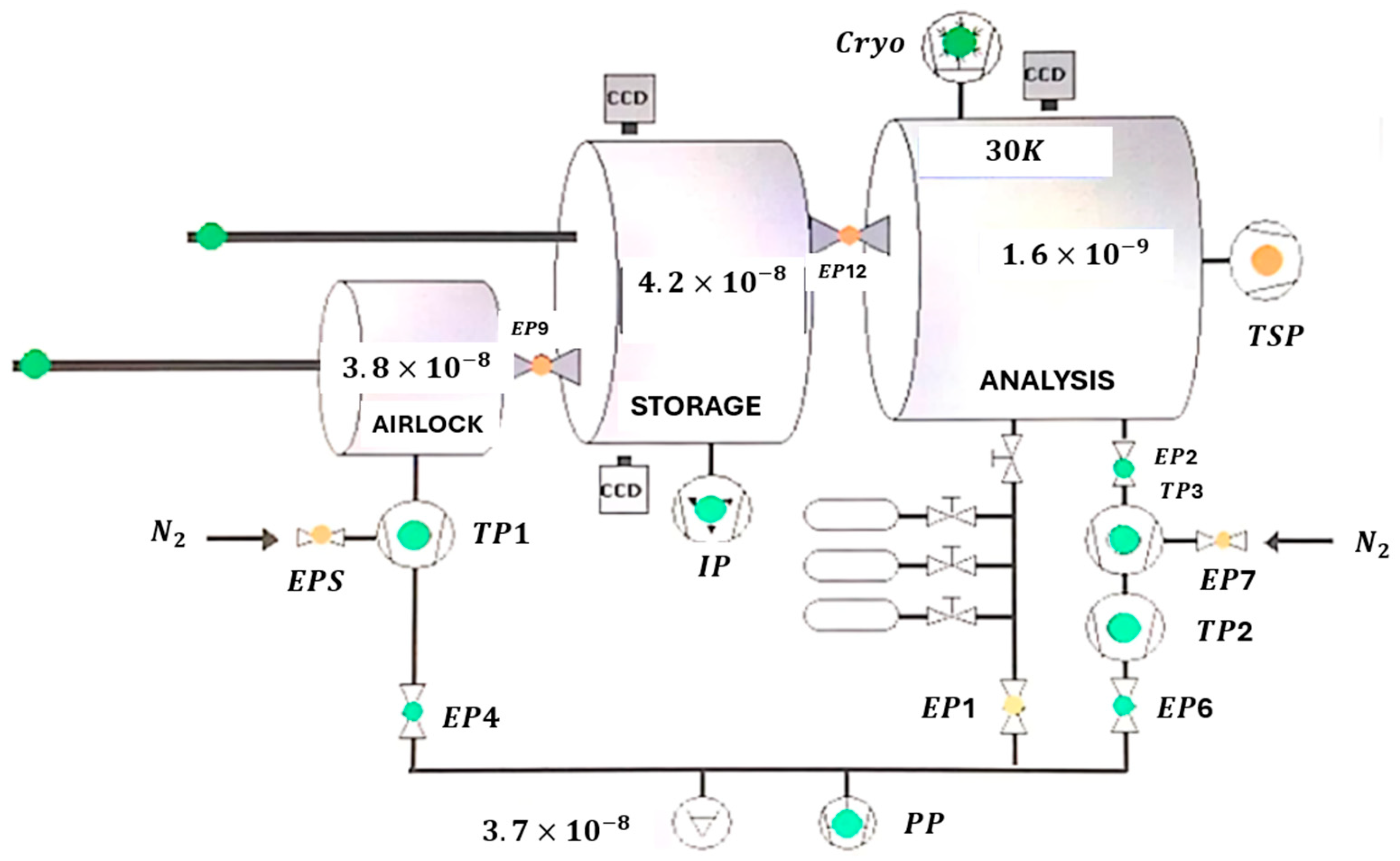
3. Methodology
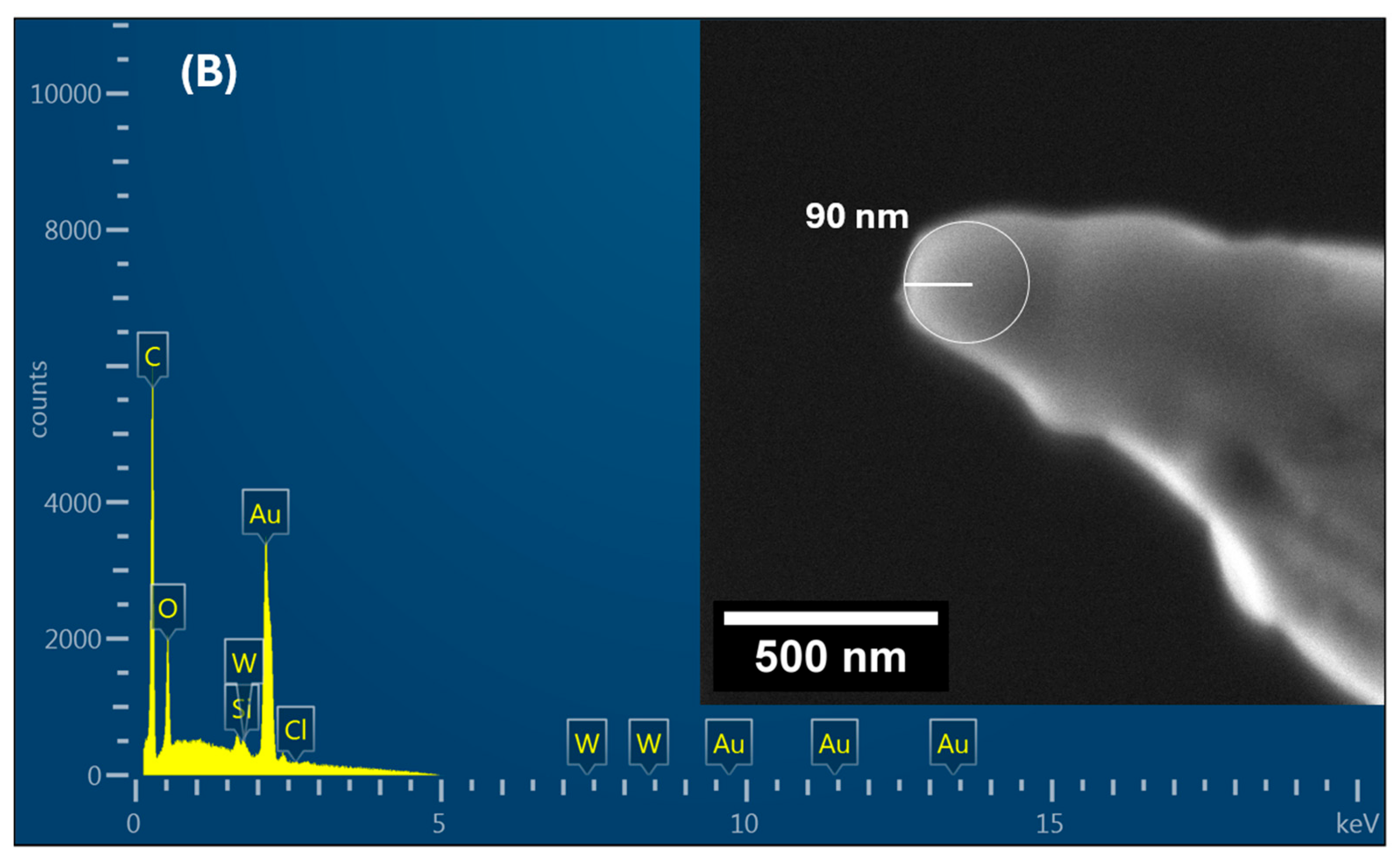
4. Characterization
5. Results and Discussion
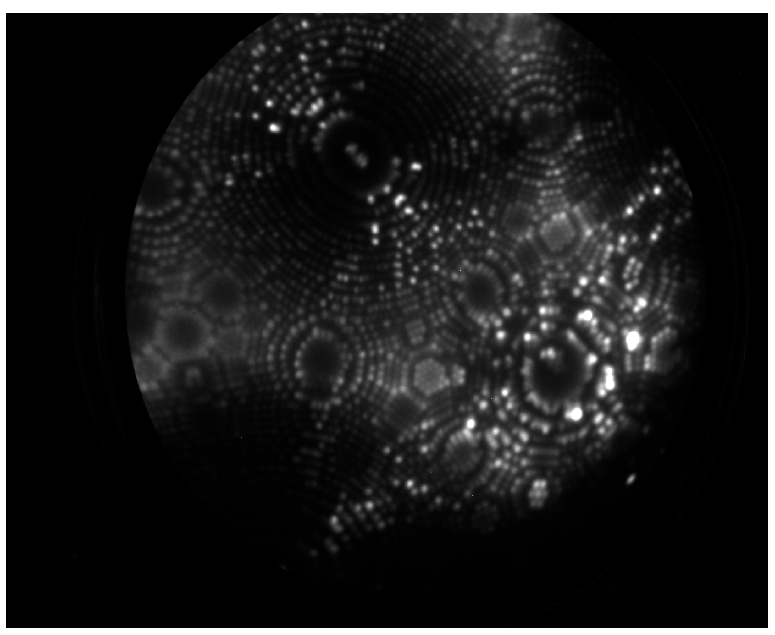
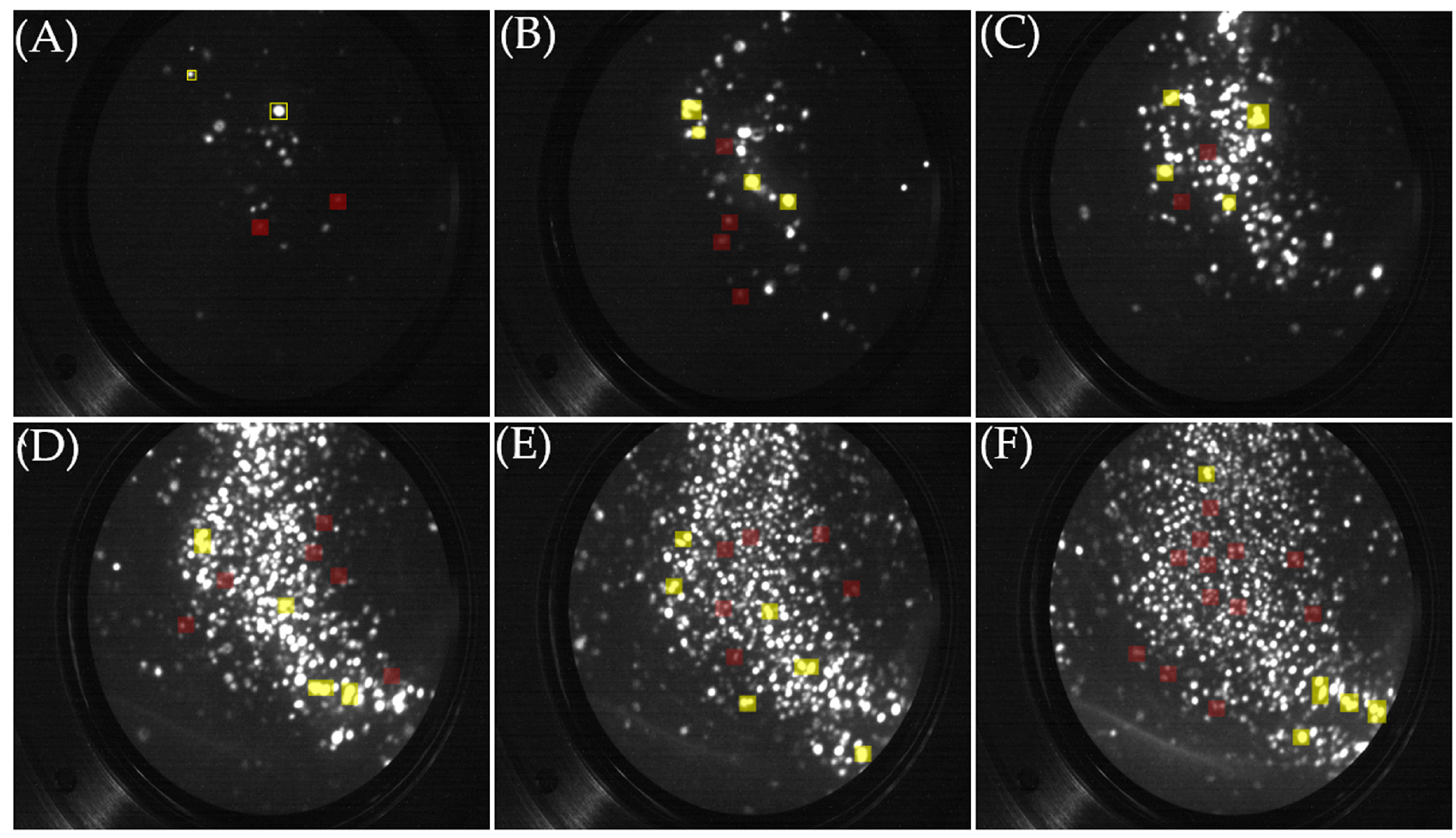
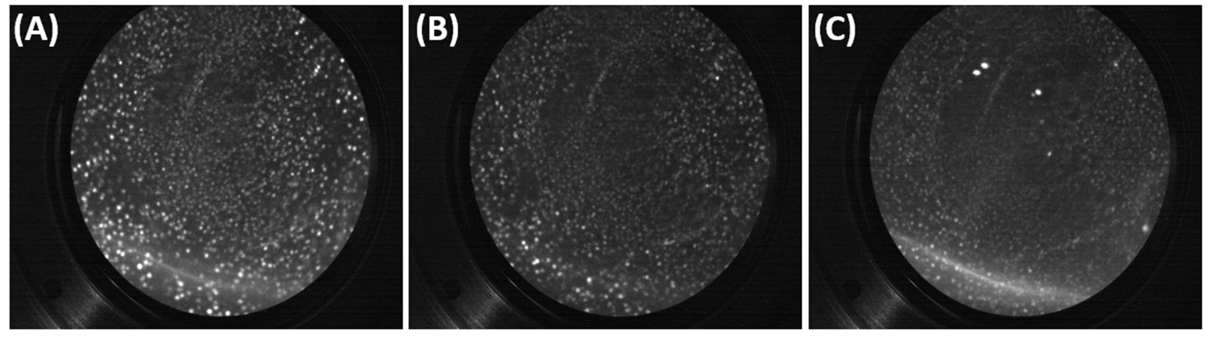
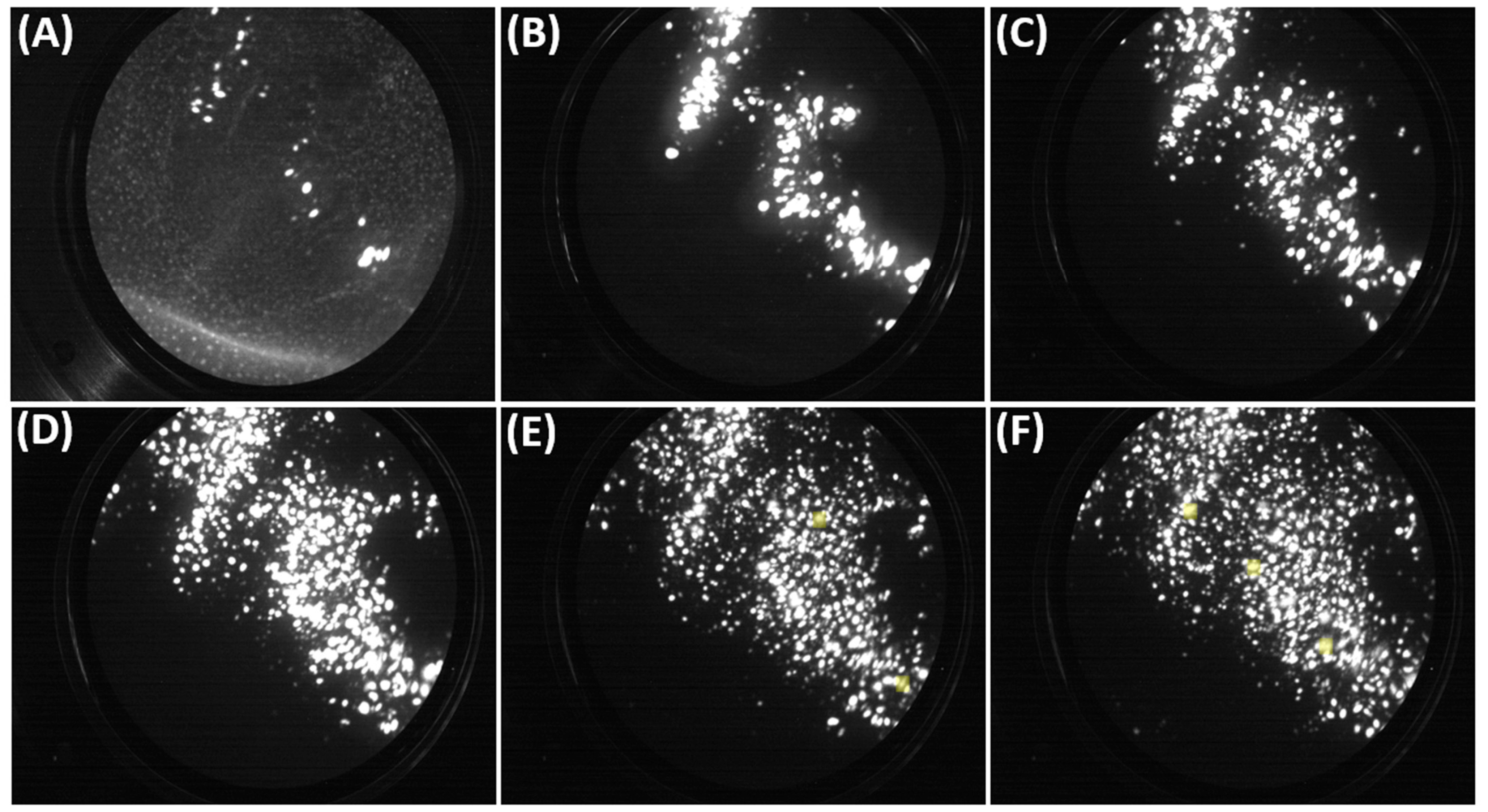
5.1. FIM Results
5.2. Atom Probe Tomography Analysis
6. Conclusions
Author Contributions
Funding
Institutional Review Board Statement
Informed Consent Statement
Data Availability Statement
Acknowledgments
Conflicts of Interest
References
- Alsoud, A.; Mousa, M.S.; Abuamr, A.M.; Fawaeer, S.H.; Ronoh, K.; AlQaisi, A.F.; Liedermann, K.; Knápek, A.; Al-Akhras, M.-A.H.; Sobola, D. Field Electron Emission from a Tungsten Cathode Coated with Silica. Jordan J. Phys. 2024, 17, 187–196. [Google Scholar] [CrossRef]
- Latham, R.V.; Mousa, M.S. Hot electron emission from composite metal-insulator micropoint cathodes. J. Phys. D Appl. Phys. 1986, 19, 699–713. [Google Scholar] [CrossRef]
- Forbes, R.G.; Deane, J.H.B.; Fischer, A.; Mousa, M.S. Fowler-Nordheim Plot Analysis: A Progress Report. arXiv 2015, arXiv:1504.06134. [Google Scholar]
- Shao, X.; Khursheed, A. A Review Paper on “Graphene Field Emission for Electron Microscopy”. Appl. Sci. 2018, 8, 868. [Google Scholar] [CrossRef]
- Chen, L.; Yu, H.; Zhong, J.; Wu, J.; Su, W. Graphene based hybrid/composite for electron field emission: A review. J. Alloys Compd. 2018, 749, 60–84. [Google Scholar] [CrossRef]
- Winnicki, M.; Łapa, W.; Znamirowski, Z. Field Electron Emission Experiments with Cold-Sprayed Cu-SiC Composite Coatings. Coatings 2021, 11, 134. [Google Scholar] [CrossRef]
- Raimondo, M.; Naddeo, C.; Vertuccio, L.; Lafdi, K.; Sorrentino, A.; Guadagno, L. Carbon-Based Aeronautical Epoxy Nanocomposites: Effectiveness of Atomic Force Microscopy (AFM) in Investigating the Dispersion of Different Carbonaceous Nanoparticles. Polymers 2019, 11, 832. [Google Scholar] [CrossRef]
- Dai, Y.; Xu, Y.; Shi, C.; Liu, Y.; Bi, S. Formation mechanism and functional properties of walnut protein isolate and soy protein isolate nanoparticles using the pH-cycle technology. Front. Nutr. 2023, 10, 1135048. [Google Scholar] [CrossRef]
- Jaber, A.M.D.; Alsoud, A.; Al-Bashaish, S.R.; Al Dmour, H.; Mousa, M.S.; Trčka, T.; Holcman, V.; Sobola, D. Electron Energy-Loss Spectroscopy Method for Thin-Film Thickness Calculations with a Low Incident Energy Electron Beam. Technologies 2024, 12, 87. [Google Scholar] [CrossRef]
- Boll, T.; Al-Kassab, T.; Yuan, Y.; Liu, Z. Investigation of the site occupation of atoms in pure and doped intermetallic. Ultramicroscopy 2007, 107, 796–801. [Google Scholar] [CrossRef]
- Müller, E.; Tsong, T. Field ion microscopy, field ionization and field evaporation. Prog. Surf. Sci. 1974, 4, 1–139. [Google Scholar] [CrossRef]
- Hashizume, T.; Wang, X.-D.; Nishina, Y.; Shinohara, H.; Saito, Y.; Kuk, Y.K.Y.; Sakurai, T.S.T. Field Ion-Scanning Tunneling Microscopy Study of C60 on the Si(100) Surface. Jpn. J. Appl. Phys. 1992, 31, L880. [Google Scholar] [CrossRef]
- Maris, H.J.; Seidel, G.M.; Stein, D. Dark Matter Detection Using Helium Evaporation and Field Ionization Stein. Phys. Rev. Lett. 2017, 119, 181303. [Google Scholar] [CrossRef] [PubMed]
- Lagally, M.G. Atom Motion on Surfaces. Phys. Today 1993, 46, 24–31. [Google Scholar] [CrossRef]
- Viskadouros, G.M.; Stylianakis, M.M.; Kymakis, E.; Stratakis, E. Enhanced Field Emission from Reduced Graphene Oxide Polymer Composites. ACS Appl. Mater. Interfaces 2013, 6, 388–393. [Google Scholar] [CrossRef]
- Al Soud, A.; Knapek, A.; Mousa, M.S. Analysis of the Various Effects of Coating W Tips with Dielectric Epoxylite 478 Resin or UPR-4 Resin Coatings under Similar Operational Conditions. Jordan J. Phys. 2020, 13, 191–199. [Google Scholar] [CrossRef]
- Panda, K.; Hyeok, J.J.; Park, J.Y.; Sankaran, K.J.; Balakrishnan, S.; Lin, I.-N. Nanoscale investigation of enhanced electron field emission for silver ion implanted/post-annealed ultrananocrystalline diamond films. Sci. Rep. 2017, 7, 16325. [Google Scholar] [CrossRef]
- Li, J.; Wang, Y.; Ran, Z.; Yao, H.; Du, B.; Takada, T. Molecular Structure Modulated Trap Distribution and Carrier Migration in Fluorinated Epoxy Resin. Molecules 2020, 25, 3071. [Google Scholar] [CrossRef]
- Ji, Q.; Wang, B.; Zheng, Y.; Zeng, F.; Lu, B. Field emission performance of bulk graphene. Diam. Relat. Mater. 2022, 124, 108940. [Google Scholar] [CrossRef]
- Knápek, A.; Allaham, M.M.; Burda, D.; Sobola, D.; Drozd, M.; Horáček, M. Explanation of the quasi-harmonic field emission behaviour observed on epoxy-coated polymer graphite cathodes. Mater. Today Commun. 2023, 34, 105270. [Google Scholar] [CrossRef]
- Abuamr, A.M.; Mousa, M.S.; Al-Bashaish, S.R.; Madanat, M.A.; AlSoud, A.; Jaber, A.M.D.; AlQaisi, A.F.; Al-Anber, M.A.; Barzinjy, A.A.; Arrasheed, E.A.; et al. Characterization of field emission from oxidized copper emitters. Phys. Scr. 2024, 99, 105029. [Google Scholar] [CrossRef]
- Mousa, M.; Karpowicz, A.; Surma, S. ‘Switch-on’ phenomena in field-electron and field-ion microscopy. Vacuum 1994, 45, 249–254. [Google Scholar] [CrossRef]
- Velikodnaya, O.A.; Gurin, V.A.; Gurin, I.V.; Kolosenko, V.V.; Ksenofontov, V.A.; Mikhailovskij, I.M.; Sadanov, E.V.; Bukolov, A.N.; Mazilov, A.A. Multi-emitter field ion source based on a nanostructural carbon material. Tech. Phys. Lett. 2007, 33, 583–585. [Google Scholar] [CrossRef]
- Oberdorfer, C.; Schmitz, G. On the Field Evaporation Behavior of Dielectric Materials in Three-Dimensional Atom Probe: A Numeric Simulation. Microsc. Microanal. 2010, 17, 15–25. [Google Scholar] [CrossRef] [PubMed]
- Bliznyuk, V.N.; LaJeunesse, D.; Boseman, A. Application of helium ion microscopy to nanostructured polymer materials. Nanotechnol. Rev. 2014, 3, 361–387. [Google Scholar] [CrossRef]
- Soud, A.A.; Buqain, R.N.A.; Mousa, M.S. Composite Metallic Nano Emitters Coated with a Layer of Insulator Covered by Au. Jordan J. Phys. 2020, 13, 253–262. [Google Scholar]
- Lunk, H.-J.; Hartl, H. Discovery, properties and applications of tungsten and its inorganic compounds. ChemTexts 2019, 5, 15. [Google Scholar] [CrossRef]
- Knápek, A.; Sýkora, J.; Chlumská, J.; Sobola, D. Programmable set-up for electrochemical preparation of STM tips and ultra-sharp field emission cathodes. Microelectron. Eng. 2017, 173, 42–47. [Google Scholar] [CrossRef]
- Allaham, M.M. Comprehensive Analysis of E478 Single-Component Epoxy Resin and Tungsten-E478 Interface for Metallic-Polymer Composite Electron Source Applications. ACS Omega 2024, 9, 30975–30985. [Google Scholar] [CrossRef]
- Boll, T.; Unocic, K.A.; Pint, B.A.; Stiller, K. Interfaces in Oxides Formed on NiAlCr Doped with Y, Hf, Ti, and B. Microsc. Microanal. 2017, 23, 396–403. [Google Scholar] [CrossRef]
- Bogdanowicz, J.; Kumar, A.; Fleischmann, C.; Gilbert, M.; Houard, J.; Vella, A.; Vandervorst, W. Laser-assisted atom probe tomography of semiconductors: The impact of the focused-ion beam specimen preparation. Ultramicroscopy 2018, 188, 19–23. [Google Scholar] [CrossRef] [PubMed]
- Seol, J.B.; Kwak, C.M.; Han, J.C.; Baek, K.H.; Jeong, Y.K. Correlative transmission electron microscopy and atom probe tomography on field evaporation mechanism of a bulk LaAlO3 oxide. Appl. Surf. Sci. 2019, 479, 828–834. [Google Scholar] [CrossRef]
- Seol, J.-B.; Kim, Y.-T.; Kim, B.-H.; Park, C.-G. Novel approach for observing the asymmetrical evolution and the compositional nonuniformity of laser pulsed atom probe tomography of a single ZnO nanowire. Met. Mater. Int. 2016, 22, 34–40. [Google Scholar] [CrossRef]
- Ivchenko, V.A. Atomic Structure of the Pt Surface after Bombardment with Ar+ Ions (E~30 keV). Adv. Mater. Phys. Chem. 2023, 13, 77–84. [Google Scholar] [CrossRef]
- Al Soud, A.; Daradkeh, S.I.; Knápek, A.; Holcman, V.; Sobola, D. Electrical characteristics of different concentration of silica nanoparticles embedded in epoxy resin. Phys. Scr. 2023, 98, 125520. [Google Scholar] [CrossRef]
- Allaham, M.M.; Forbes, R.G.; Knápek, A.; Sobola, D.; Burda, D.; Sedlák, P.; Mousa, M.S. Interpretation of field emission current–voltage data: Background theory and detailed simulation testing of a user-friendly webtool. Mater. Today Commun. 2022, 31, 103654. [Google Scholar] [CrossRef]
- Cheng, Y.; Yu, G. Effects of Varying Nano-Montmorillonoid Content on the Epoxy Dielectric Conductivity. Molecules 2024, 29, 4650. [Google Scholar] [CrossRef]
- AlSoud, A.; Daradkeh, S.I.; Shaheen, A.A.; Al-Hroub, Q.A.; Knápek, A.; Mousa, M.S.; Sobola, D. Electrical properties of epoxy/graphite flakes microcomposite at the percolation threshold concentration. Phys. Scr. 2024, 99, 055955. [Google Scholar] [CrossRef]
- Alsoud, A.; Daradkeh, S.I.; Al-Bashaish, S.R.; Shaheen, A.A.; Jaber, A.M.D.; Abuamr, A.M.; Mousa, M.S.; Holcman, V. Electrical Characterization of Epoxy Nanocomposite under High DC Voltage. Polymers 2024, 16, 963. [Google Scholar] [CrossRef]


Disclaimer/Publisher’s Note: The statements, opinions and data contained in all publications are solely those of the individual author(s) and contributor(s) and not of MDPI and/or the editor(s). MDPI and/or the editor(s) disclaim responsibility for any injury to people or property resulting from any ideas, methods, instructions or products referred to in the content. |
© 2024 by the authors. Licensee MDPI, Basel, Switzerland. This article is an open access article distributed under the terms and conditions of the Creative Commons Attribution (CC BY) license (https://creativecommons.org/licenses/by/4.0/).
Share and Cite
Sobola, D.; Alsoud, A.; Knápek, A.; Hamasha, S.M.; Mousa, M.S.; Schubert, R.; Kočková, P.; Škarvada, P. Field Ion Microscopy of Tungsten Nano-Tips Coated with Thin Layer of Epoxy Resin. Technologies 2024, 12, 193. https://doi.org/10.3390/technologies12100193
Sobola D, Alsoud A, Knápek A, Hamasha SM, Mousa MS, Schubert R, Kočková P, Škarvada P. Field Ion Microscopy of Tungsten Nano-Tips Coated with Thin Layer of Epoxy Resin. Technologies. 2024; 12(10):193. https://doi.org/10.3390/technologies12100193
Chicago/Turabian StyleSobola, Dinara, Ammar Alsoud, Alexandr Knápek, Safeia M. Hamasha, Marwan S. Mousa, Richard Schubert, Pavla Kočková, and Pavel Škarvada. 2024. "Field Ion Microscopy of Tungsten Nano-Tips Coated with Thin Layer of Epoxy Resin" Technologies 12, no. 10: 193. https://doi.org/10.3390/technologies12100193