Abstract
The firmware developed for the readout and trigger processing of the information emerging from the BIS78-RPC Muon Spectrometer chambers in the ATLAS experiment at CERN is presented here, together with data processing techniques, data acquisition software, and tests of the readout chain system, which represent efforts to make these chambers operational in the ATLAS experiment. This work is performed in the context of the BIS78-RPC project, which deals with the pilot deployment of a new generation of sMDT+RPCs in the experiment. Such chambers are planned to be fully deployed in the whole barrel inner layer of the Muon Spectrometer during the Phase II upgrade of the ATLAS experiment. On-chamber front-ends include an amplifier, a discriminator ASIC, and an LVDS transmitter. The signal is digitized by CERN HPTDC chips and then processed by an FPGA, which is the heart of the readout and trigger processing, using various techniques.
1. Introduction
New integrated sMDT (Small Monitored Drift) chambers + RPCs (Resistive Plate Chambers) are installed at the outer end of the ATLAS BI (“Barrel Inner”) layer, in the barrel-endcap transition region, at , where is the pseudorapidity. (Pseudorapidity is defined as , with indicating the polar angle with respect to the beam axis). This region is characterized by very high background rates, and the “BIS78” (Barrel Inner Small 7 and 8) RPCs and sMDT chambers are designed to suppress this background without sacrificing efficiency for finding muons.
During the “Phase I” upgrade, which preceded the Run-3 data-taking period of ATLAS (2022–2025), only the 8 “side A” sectors were installed, see Figure 1. These chambers are compatible with HL-LHC (High Luminosity–Large Hadron Collider) conditions [1,2], and thus, during the next (“Phase II”) upgrade, such chambers will also be installed in the other side of ATLAS (“side C”). During the Run-3 period, only the BIS78 RPCs (not the sMDT chambers) will provide muon candidates for the trigger system (“trigger candidates”). BIS78 RPCs consist of a triplet of new-generation 1 mm gas-gap RPCs providing 3 layers of and orthogonal coordinates and an efficient stand-alone trigger coincidence. The resulting chamber surface is about 31 m2 including sides A and C, for a total RPC detector area of about 94 m2. Photographs from the installation procedure of the BIS78 stations performed on 17 September 2020 by the ATLAS Collaboration are in [3].
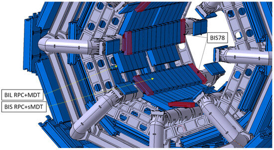
Figure 1.
RPC upgrades in ATLAS inner barrel (BI region). The new BIS78 chamber triplets (red) were installed on side A for the Phase I upgrade and represent about 5% of the full BI region, which will be upgraded in Phase II by installing RPC triplets as well.
The original RPCs, deployed since the beginning of ATLAS, are mentioned here as a comparison and in order to put the BIS78 chambers in context. The original RPCs represent the bulk of the RPC system for the full lifetime of ATLAS. This system is arranged in three concentric layers of doublet chambers around the beam axis, providing six independent measurements along the muon track with a spatial resolution of about 1 cm and a time resolution of about 1 ns. A doublet chamber has two sensitive gas planes, each read out by orthogonal and strips. Two of the three doublet layers of RPCs are mounted on both sides of the MDT chambers in the “middle barrel” (BM), the third doublet layer is mounted on one side of the outer MDT chambers (in the “outer barrel”, BO). In this arrangement, there are no trigger chambers in the innermost barrel layer (BI), as described in [1]. More details on the original RPC system can be found in [4].
As mentioned above, the BIS78 chambers are a new type of RPC gaseous detector, which during Run-3 serves as a pilot project for the next major ATLAS upgrade, the so-called Phase II. At that time, the system of BIS RPCs will be completed and the naming of the detectors will be BIS from 1 to 6. In addition, new BIL (Barrel Inner Large) detectors will be installed. The main differences in BIS (and BIL) compared to the original RPCs are as follows:
- Thinner gas gap at 1 mm (the original RPCs have 2 mm);
- Lower operating high voltage, at 5400 V compared to 9600 V;
- New generation Si-Ge with higher-gain, low-noise front-end electronics.
Benefits are the reduced chamber envelope, higher rate capability, improved time resolution from about 1.1 ns to 0.4 ns, and reduced total charge per hit generated in the gas for a given efficiency. BIS78 chambers are organized in thin triplets each providing 540 strips including both and coordinates for a total number of strips of about 4320 strips for each side (8 sectors × 540 strips/sector). A complete description of this new generation of RPC detectors as well as the full specifications of the BIS78 project can be found in the ATLAS Muon Spectrometer Phase II Upgrade Technical Design Report [1]. A layout of the BIS78 station is shown in Figure 2.
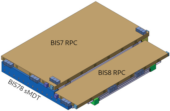
Figure 2.
A BIS78 station, consisting of a single two-multilayer sMDT chamber integrated with two BIS7 and BIS8 RPC triplets, covering the area of the original BIS7 and BIS8 MDTs within the same total thickness [1].
2. Materials and Methods
2.1. The BIS78 Data Acquisition and Control System
A schematic of the block diagram of the BIS78 Trigger and Data AcQuisition (TDAQ) Hardware Systems for Run 3 is shown in Figure 3. The picture illustrates the various components starting from the detector, to the front-end electronics, to the on-detector electronics in the ATLAS cavern where digitization, zero-suppression, triggering, and buffering is taking place, and to the FELIX system and the Software Read-out Driver, which are located in the experiment’s counting room.
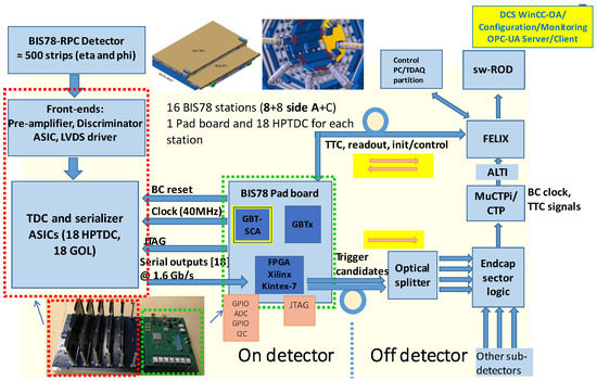
Figure 3.
The BIS78-RPC TDAQ Hardware System, including on- and off-detector electronics and TDAQ systems.
2.1.1. On-Detector Electronics
The on-detector electronics are composed of 4 parts:
- New on-detector front-end electronics: 8-channel Front-End PCBs composed of a new Amplifier (Si), a full-custom ASIC Discriminator (SiGe) and an LVDS transmitter. A set of two of these boards contains 32 channels and connects via ribbon cables to one HPTDC (High Performance Time-to-Digital Converter) [5] installed on the Mezzanine card.
- HPTDC Mezzanine boards: each one hosts 3 CERN-HPTDC digitizers and 3 CERN-GOL (Gigabit Optical Link) [6] transmitter-serializer chips.
- Motherboard (MB): hosts and holds in a vertical position 6 Mezzanine boards and connects through an HPC-FMC connector to the PAD board (see next item); thus, there are 18 HPTDC and 18 GOL ASICs in the MB + Mezzanine system.
- Trigger PAD board: the Readout and Trigger data acquisition and processing unit, based on the Xilinx Kintex-7 FPGA, model XC7K355T [7]. It features a standard rad-hard set of communication chips developed by the CERN GBT project [8] for Phase I: a GBTx ASIC and a GBT-SCA slow-control ASIC. The FPGA is communicating with the GBT-SCA chip over the protocol, which in turn connects via an e-link to the GBTx and then to the FELIX system [9], where the slow-control software runs, as described in Section 2.1.3. Optical communication with the FELIX system is handled by a VTRX transceiver, while two VTTX transmitters send trigger candidates to the End-cap Sector Logic board. Both VTRX and VTTX were developed by the CERN-coordinated Versatile Link Project [10,11].
A set of one PAD, one Motherboard and six Mezzanines is required for each Sector, for a total of eight sets used for the eight BIS78 sectors installed on side A of ATLAS. A set of these components is enclosed in an aluminum box. Figure 4 illustrates a set of these electronics as used in the ATLAS Muon lab for testing and development.
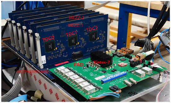
Figure 4.
BIS78-RPC Mezzanines, Motherboard, and PAD in the ATLAS Muons lab.
2.1.2. Off-Detector Electronics, Control System, and Software
The rest of the electronic boards and computers that make up the BIS78-RPC TDAQ system are the FELIX and ALTI systems, both having hardware, firmware, and software components. The FELIX (FrontEnd LInk eXchange) system consists of a FELIX server PC and a mounted BNL-712 PCI-E card [9] and handles all 8 sectors of side A. For Run 4, another FELIX system will serve the chambers to be installed on side C. The ALTI (ATLAS Local Trigger Interface) [12] is a VME-based module for timing, trigger, and control (TTC); it is based on an Artix-7 FPGA with a dedicated FW, and it is controlled/configured by a VME-crate SBC (Single Board Computer). One ALTI module per side is required.
The Detector Control System is responsible for the safe operation and monitoring of the detector infrastructure and includes the Power System, which supplies the HV/LV to the detector and the Trigger and DAQ infrastructure. For BIS78, the Power System is integrated with one of the legacy RPCs [13] and is based on the CAEN EASY system, which consists of CAEN SY-4527 mainframes [14] located in the counting room connected via a branch controller and CAN bus to HV/LV, ADC, and DAC modules installed in crates in the detector cavern.
2.1.3. TDAQ Software
For setting up, running, and monitoring the BIS78 system, the ATLAS TDAQ Framework Software [15] (version 11-02-01) is used, as it has been used for all ATLAS sub-detectors. Major components of this software are the Software Read-Out Driver (SW ROD), the GNAM online monitoring software, designed to monitor ATLAS detectors at all DataFlow levels, and a Configuration software. Customization was required and conducted so that the generic repository files are tailored to the specific requirements of the BIS78 project. The SW ROD customization identifies the Bunch-Crossing Identifier (BCID) and the Level-1 Identifier (L1ID) in the data packets and synchronizes the data streams from the different sectors and ATLAS. The GNAM samples the data acquired at Level-1 and processed by the SW ROD plugin, plotting errors, hits, and signal distributions. The configuration software leverages the OpcUASCA infrastructure to send and receive I2C and JTAG signals to and from the PAD board. A set of xml files are used to store the system configurations (both SW, FW, and HW).
Recently, a dummy HLT configuration was implemented, allowing the testing of the system and the recording of ATLAS-style data up to 690 Hz from a 22 kHz Level-1 generated rate.
Some low-level procedures are handled during development and system testing using FELIX ftools: the GBTx configuration is done with the fice tool, which reads or writes GBTX chip registers via the dedicated GBT-link IC channel. The configuration of the e-links is done with elinkconfig, which is a GUI for the link and data generator and configuration file creation. Finally, the PAD FPGA is programmed using fscajtag, a tool used to program a bit-file into a Xilinx FPGA connected to a GBT-SCA JTAG port.
In nominal conditions, programming and monitoring of PAD registers is done through a server–client architecture using an OPC-UA protocol. The BIS78 DCS and the communication with the PAD registers are handled by software implementing the OPC-UA protocol, with server–client architecture, developed by ATLAS Central DCS [9,16,17]. As with every sub-detector, custom DCS functions and GUI were developed by the team, including functionalities like low-voltage and high-voltage control, detector and electronics status, and temperature measurements. Development work is in progress to include BIS78 Bytestream converters into the ATLAS Offline Software, called Athena [18].
2.2. Data Readout Firmware
One of the most demanding parts in terms of research and development for this project, after the design of the electronics boards, has been the firmware (FW) (or gateware) for the Kintex-7 FPGA placed on the PAD board. There has been continuous development and improvement since May 2022, when a new firmware project was initiated. As mentioned before, one FPGA performs all the data-readout and, in the future, the trigger functions for one sector, which means up to 576 readout channels. The PAD board takes care of the digital data acquisition and synchronization, decoding, sorting of the data according to their BCID, selective (triggered) read-back from the storing BRAM, and data-formatting in a FELIX-appropriate format. The Functional Block Diagram displaying all the top level modules is presented in Figure 5.
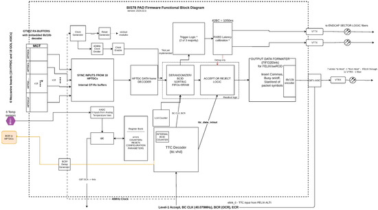
Figure 5.
Functional block diagram of the PAD FPGA (Kintex-7) firmware.
For the PAD logic to be working synchronous to the LHC clock (also called TTC clock), two basic required components are the TTC Decoder, which receives and decodes the TTC information from FELIX [19] to be then internally used, and the Clock generator, which synchronizes all the PAD logic with the TTC clock and/or to other specific clock signals generated from it.
TTC Decoder: The TTC signals are generated by the ALTI module (directly or inherited by the CTP), decoded inside FELIX, and finally transmitted over fiber to the PAD board.
Synchronous to the TTC clock, three important signals are sent by FELIX and used inside the PAD board: the Bunch Counter Reset (BCR), the Event Counter Reset (ECR), and the Level-1 Accept (L1A).
The BCR serves the purpose of resetting the bunch crossing counter, which increments with each clock cycle on the TTC 40 MHz clock. This counter, also known as BCID, is a 12-bit counter. Approximately every 89 μs, a BCR command is transmitted, aligning with the time it takes for a bunch to complete a circuit in the LHC. Within this interval, the BCID counter reaches its maximum value of 3564 counts.
The L1A communicates with the detector front-end readout systems, indicating whether to retrieve the event information stored in the front-end electronics pipelines.
The ECR is employed to increment the event reset counter, set to reset every 5 s for ATLAS. Combining the event reset counter with the L1A counter results in the Extended L1ID (EVID), a 32-bit value. The lower 24 bits contain the L1A counter, while the upper 8 bits contain the event reset counter. Upon receiving an ECR, the upper counter increases by 1, and the lower part resets to zero. With each L1A reception, the lower part increments by 1.
BCID and EVID values function as labels for the data accepted by the trigger.
A dedicated E-link, named TTC E-link, is used for transmitting the TTC information. TTC E-link is configurable, and for the BIS78 project, it runs at 320 Mbps, transferring 8 bit TTC information on every TTC clock according to Table 1.

Table 1.
List of bits sent by FELIX on the TTC E-link.
The full TTC e-link frame is transmitted from FELIX to the PAD, from the MSB (bit-7) to the LSB (bit-0). Every piece of TTC information is contained within a one-bit period, which is equivalent to 3.125 ns (the TTC signal runs at 320 MHz).
Clock Generator: Another basic component is the IP-based Clock Generator, which is connected to the 40 MHz TTC clock input from FELIX and from which all the necessary clocks are generated.
In order to sample the TTC information, a higher frequency clock is needed. For this purpose, the Clock Generator is used to create a 320 MHz clock. The clock is delayed by 1.5625 ns with respect to the incoming TTC clock and thus to the TTC stream in order to correctly decode the TTC incoming data. Since the TTC stream is output with this delay, all the other internal clocks used to elaborate this information are delayed by the same time (1.5625 ns) in order to be aligned to it.
A delayed version of the 40 MHz clock is used for the TTC configuration block and for the L1A and the EVID counters, whereas a further 40 MHz 180° shifted clock is used to send a delayed version of the BCR to the HPTDC. The delay value, which corresponds to 12.5 ns, has been chosen in order to respect the HPTDC specifications.
The Clock Generator generates three extra higher-frequency clocks, at 80 MHz, 160 MHz, and 320 MHz, in phase with the TTC-delayed clock. The 80 MHz clock is used by the deserializers, whereas the 160 MHz and the 320 MHz clocka are used to speed up the remaining logic (the Readout Logic and Output Data Encoder, respectively). The Clock Generator has a locked signal output, which indicates that the component is producing stable and reliable clocks. For this reason, the locked signal is used as an active low reset for all the PAD logic.
Deserializer (GTX) and HPTDC Data Decoder: The HPTDC’s output data frame format, which is fed into the GTXs, is illustrated in Figure 6. This output data frame consists of 32 bits transmitted every 25 ns (40 MHz rate), containing the following fields: the HPTDC header (the four most significant bits of the frame). Normally, the HPTDC header is set to the constant binary value “0100”, which indicates the HPTDC is working without errors in pairing mode. However, if the HPTDC detects an error condition, the HPTDC header is set to the binary value of “0110”. Additionally, the frame includes the channel ID (identifying each of the 32 channels read from each HPTDC), the TDC ID (identifying the HPTDC), the hit width and leading time values, and the BCID (Bunch Identifier). As already mentioned, the hit data coming from 18 HPDTCs are serialized and 8B/10B encoded by the GOL ASIC before being transmitted to the PAD at 1.6 Gbps. On the PAD board, 18 GTX Gigabit Transceivers (a commonly used transceiver technology provided by Xilinx) are employed for the deserialization process. To minimize power consumption, the GTXs are configured with Receiver (Rx) only, as the transmitter part is not used. The internal Rx buffer as well as the 8B/10B decoder are enabled to achieve alignment and synchronization and to decode input data. Moreover, to reduce latency, the GTXs have been configured to serialize a 16-bit word every 50 ns (80 MHz).
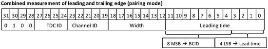
Figure 6.
HPTDC ASIC: Data frame format in pairing mode [5].
The GTX 16-bit parallel words are then processed by the HPTDC Data Decoder block which, by looking at the 8B/10B comma words (corresponding to the hexadecimal values “50bc” and “c5bc”), is able to correctly align two consecutive words to reconstruct the 32-bit HPTDC frame (Figure 6). The reformatted 32-bit words are then sent to the next block, the Readout Logic.
Readout Logic: In the readout block, the input data are stored in two types of FIFOs and a Block RAM (BRAM). The logic can work in two modes: “pass-through”, where all data are sent out, or L1A-information based, which means that only when an L1-Accept signal arrives, data with the appropriate BCID tag are sent to the next block, where they are formatted and transmitted to FELIX via an optical link. In normal ATLAS runs, the L1A signal is issued by the Central Trigger Processor, the CTP.
According to the hardware structure described in Section 2.1.1, the readout logic consists of six replicas of the Readout block, each processing data coming from one mezzanine, i.e., from three HPTDCs.
Three 32-bit TDC-FIFOs are used to store the decoded output data of three HPTDC chips. Then, the HTPDC header of each frame is checked to validate the data. If the header is “0100” (as shown in Figure 6), the data are considered reliable and transferred to an additional TDC-FIFO, common to all HPTDCs. If the header indicates an error (set to “0110”), the data are discarded, and an error monitor counter is incremented.
The DATA-BRAM, 32-bit wide and 8192 locations deep, functions as a derandomizer controlled by the Readout Finite State Machine (FSM). Indeed, the Readout FSM manages writing and reading to/from the DATA-BRAM. It ensures that hits related to the same BCID are stored in consecutive locations within DATA-RAM. Up to 32 possible locations per BCID are available, corresponding to the maximum hit multiplicity expected under normal conditions. The dimensions of the DATA-RAM are chosen to safely store hits belonging to up to 256 BC (i.e., 6400 ns) before they are possibly selected.
In order to select the data with the appropriate BCID tag, very important is the information stored in the 44-bit L1A-FIFO. In the L1A-FIFIO, the L1ID and BCID values at which an L1A signal arrives are stored. Starting from the stored BCID and knowing the L1A signal latency, the Readout FSM calculates the readout BCID, so that it can read from DATA-RAM the data corresponding to the readout BCID up to the next following 6 BCID. The maximum value of BCID to be sent out is selected by the readout window parameter, and it has been chosen to facilitate the calibration of the detector during commissioning.
Output data format: The data formatting is handled by the Readout FSM. The data format is shown in Figure 7. For each L1A signal received, data corresponding to up to 6 consecutive BCID can be sent. This stream consists of a variable number of 16-bit width words, depending on the number of hits and the selected readout window width. The 16-bit width size has been chosen to fit the width constraint of the FIFO2elink module, which is going to be described in the next section.
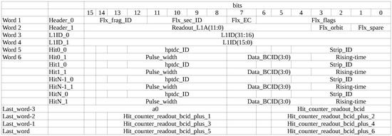
Figure 7.
FPGA output data format as transmitted to FELIX.
For each communication to FELIX, via the e-links, two header words (Header_0 and Header_1) are necessary, containing specific FELIX ID identifiers and information, among which the 12-bit readout BCID value plays a fundamental role in the data reconstruction. The next two words contain the 32-bit EVID. The EVID is eventually followed by the HPTDC data belonging to the readout window, up to the Last_word-2. Two words per each HPTDC data are necessary. The data are followed by a footer block, which starts with the “a0” hexadecimal symbol and contains information on how many hits per BCID (in the readout window) have been sent. The range is from the first readout BCID called BCID0, up to BCID0 + 6, which represents the last BCID in the readout window.
The SW ROD plugin, which is custom-made for this project, as for other ATLAS sub-detectors separately, can be programmed to store the whole data input to it or discard some parts.
Output Data Encoder (FIFO2elink): From each readout block, the outputted formatted data need to be sent to FELIX using one of the available e-links.
The FIFO2elink module is used to encode the data according to the 8B/10B protocol before being sent to FELIX (optical communication over VTRX). The module is part of the ATLAS FELIX Project Firmware, released as open-source in [10]. The related sources of firmware have been modified as required to fit the needs of the PAD board. The output rate is locked to 320 Mbps per e-link, for a total of 6 data e-links. After that, the data stream is processed by the GBTx ASIC, which is configured to GBT mode, and the data are eventually organized in 120-bit wide output frames. A separate e-link for monitoring purposes is considered for future implementation.
Trigger Logic: At the time of writing this document, this part is under development. Here, the signal is sourced from the Readout, and the data words—selected by L1A info—are processed based on the 2-out-of-3 majority simple algorithm. Thus, when a traversing muon hits one layer, incident within a wide range of angles, also a hit would be expected on one or both of two other layers. If at least two (or all three) layers have a hit, in strips with close proximity between them, this means that the hit is valid. The data that correspond to these hits can be read-out from the Readout FIFOs and BRAM. Eventually, only this trigger information contained in the data words, forms the so called trigger candidates and will be sent via two fibers, using the two VTTX transmitters of the PAD to the End-cap Sector Logic electronics.
One last step remains: to adjust the output data to the End-cap Sector Logic at a fixed latency. This requirement is set by the Experiment’s Trigger sub-system and should be exactly 42 BCs or 1050 nanoseconds.
Configuration via GBT-SCA and Register Bank: A set of configuration registers, which control FW parameters like BCID offset, TTC offset, and Readout mode, as well as other registers used as counters such as the TTC signal rate counter and the HTPDC error counter are implemented in the FPGA. During development—before functionality was implemented—most of these parameters and configurations were set or read by using VIOs in Vivado. For system testing, a C++ tool called I2C_scope is used to execute configuration and monitoring actions over .
Simulation waveforms are shown in Figure 8 and Figure 9. In these figures, the random inputs corresponding to 3 different HPTDCs are generated. There is one generated input L1A signal. Also, the process of writing/reading the data into/out of the FIFOs and the BRAM is shown.
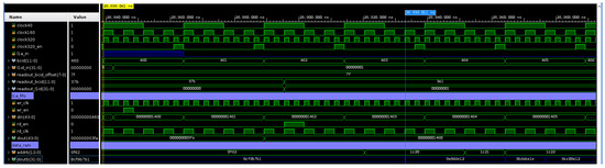
Figure 8.
Simulation with generated data for 3 HPTDCs and one Level-1 Accept signal. The data are stored in the L1A fifo, and the doutb signal is the BRAM output.
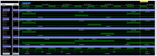
Figure 9.
In these simulation waveforms, the data stored in the tdc0, tdc1, tdc2, and tdc012 FIFOs are displayed.
Resource Utilization
The resources used on the FPGA device are displayed in Figure 10 as reported by Vivado 2021.2 with the vast majority of the Readout firmware implemented and with minimal ILA usage.
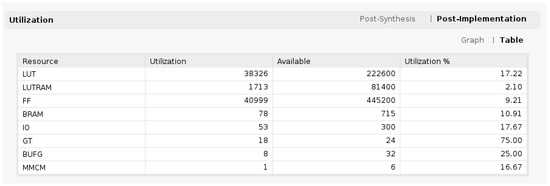
Figure 10.
Resource utilization on the Kintex-7 as reported by Vivado (February 2024).
All the values are below 50%, except for the GTX receivers (but their number is final). Also, the total on-chip power reported is 5.494 W. As an indirect comparison, the PAD board, which hosts the FPGA, has a measured consumption of 11.5 W for sector A4 and 12.5 W for sector A14.
3. Results and Discussion
3.1. Firmware and Software Testing in the ATLAS TDAQ Frame
3.1.1. Testing at the Muon Lab
All the Muon lab tests were done using a FELIX server with a BNL-712 card, an ALTI module controlled by its corresponding SBC on the same VME crate, and power supplies (testbench and VME crate–based). Low voltages were set to 8 volts for the MB and PAD. Programming of the PAD was done with the popular Xilinx Platform Cable USB II, using JTAG. For real data produced by “hits” (signals) from cosmic radiation muons, two types of signal sources were used. In the first setup, data were from a BIS7/BIS8/BIL RPC detector with mounted front-end electronics; in this case, we can have up to 6 × 32 channels per chamber. Most of the time, the used inputs were in the range of one to three Mezzanine cards (equivalent to: between one and nine HPTDCs). In a different setup, we used 6 scintillators with one output channel for each one, having 6 output channels in total. These signals were used to pulse six discrete channels. Often, the option of pulsing just one or two channels as a sanity test was also used. In all cases, the analog LVDS signals were driven into the inputs of the Mezzanine card(s) with parallel ribbon cables.
The functionality concerning the Trigger, Timing, and Control (TTC) signals was tested during summer 2022 in the lab, where the clock and the source of TTC signals was the lab’s ALTI module. Various patterns containing L1A signals as well as various counter-reset signals (BCR/OCR/ECR) were sent via the ALTI, received by the BIS78 electronics, and displayed on Vivado ILAs, verifying the correct acquisition and decoding of these signals. Both the Decoder and the Readout have been first simulated in Vivado, with appropriate testbenches and dummy/generated input data that resemble real HPTDC data frames. Additionally, these blocks were tested with detector signals. A critical step was to map the HPTDC ID (number) to the GTX receiver, as this part of the FW is implemented by Vivado—not controlled by the RTL developer. Also very important were the checks for correct connectivity and data integrity; for this, ILAs were monitored together with triggering for error words. These words start with 6xxx, and ideally we expect none of those to appear. Also, on the ILAs, checks were done to reassure that the first 16 bits of the data words are within the range 40xx–4fxx, which means they represent actual chip data—not junk data.
3.1.2. Testing at Point 1
In the system tests during January 2024 in the ATLAS Point 1 environment, the latest available version of the TDAQ software, as described in Section 2.1.3, was used. Naturally, all the on- and off-detector electronics as well as the other parts of the TDAQ and DCS system remained unchanged, unlike the software and firmware, which keep evolving. While the data-taking sessions (the “runs”) were activated and controlled through an IGUI tool, part of the TDAQ framework [15] (and in particular the SW ROD and GNAM applications) was running in the back-end, recording data, and producing real-time histograms, respectively.
The standard testbeds for FW and SW were the BIS78 sectors A04 and A08. Procedures followed on these sectors provide a guide and reference for testing the rest of the sectors as well as the system as a whole. Using this setup, test data were recorded and histograms were produced that demonstrated the FW and SW functionality on specific sectors, the A04, A08, and A14 sectors more recently. Histogram processing is done using the widespread ROOT framework [20].
The test runs were taken with the following settings: the ALTI module was operated in standalone mode, without any signaling from the ATLAS Central Trigger Processor (CTP), using a pattern file, with one typical BCR signal and two L1A signals per orbit, which yielded a 22 kHz Level-1 rate, and an ECR signal every 5 s (the usual setting for ATLAS running). Since the end of October 2023, the LHC complex has been in the “2023 Year-End-Technical-Stop” (YETS) period. Thus, the data for these tests (January 2024) were noise from the chambers, and the only source of real particles was the sporadic cosmic radiation. Events were captured for 3 min during which both sectors and all of the TDAQ system was running smoothly. This way, the GNAM application produced histograms showing hits per HPTDC chip and per channel for the A12 and A14 sectors, demonstrating that the readout chain works as expected. All ROOT files and logs from the SW ROD and GNAM applications were copied and saved for long-term storage in the CERN EOS storage [21]. Given that Point 1 system testing involves all the components, from detectors to cables to all kinds of electronics and software, it can be considered as a fully fledged testing environment for every aspect of the RPC-BIS78 system.
All the Point 1-related development and testing procedures are executed with the goal and prospect of proper integration with the rest of the ATLAS subsystems. At that phase, all 8 BIS78 sectors will be included in the ATLAS combined runs, receiving their signaling and clocking directly from the Central Trigger Processor and running synchronously with all the other sub-detectors. A very useful functionality in such runs is the BUSY signal, which indicates that the internal buffering of the BIS78 readout is full. This part remains to be developed.
3.2. Conclusions
This work describes mostly the Firmware development for the RPC-BIS78. A new TTC signal-based readout mechanism is implemented including the standard ATLAS TTC signals, namely, L1A and ECR signals. Also implemented are a unified readout FSM that sends data in a new output data format, which is able to contain multiple hits from several HPTDCs. In the software domain, customization of the SW ROD and the GNAM was done and also many configuration files have been prepared. In the last year, a lot of testing of the above R&D has been performed with BIS78 sectors inside ATLAS, using cosmic radiation as the source.
3.3. Future plans
Debugging, which is a crucial part of system integration in Point 1, is ongoing for the RPC-BIS78 system. Driven by the requirements of the ATLAS Experiment for Run 3 and as the pilot role of the project, the goal for the BIS78-RPC system is to be soon included in the ATLAS combined runs, thus operating synchronous with the rest of the ATLAS sub-detectors. Regarding the next years, the BIS78-RPC electronics and firmware will be in operation for the duration of CERN’s LHC Run 3, but they will be upgraded (replaced) for the Phase II upgrade of ATLAS, which will start in 2026-27.
Author Contributions
A.V. has worked on Firmware Development and Simulations, Bench Testing, System Testing, and Documentation. K.K. has worked on System Testing. F.L. has worked on the TDAQ Software and System Testing. S.P. has worked on Firmware Development and Simulations and System Testing. A.P. has worked on the Infrastructure Setup, TDAQ, and DCS. R.V. has worked on Board Design, Firmware Development, and Simulations. All authors have read and agreed to the published version of the manuscript.
Funding
This research has been part of the ATLAS Experiment and thus funded by the ATLAS Collaboration.
Institutional Review Board Statement
Not applicable.
Informed Consent Statement
Not applicable.
Data Availability Statement
Data in [6,12] are available with permission from CERN (https://proj-gol.web.cern.ch and https://twiki.cern.ch/twiki/bin/view/Atlas/LevelOneCentralTriggerALTI) (accessed on 30 May 2024). The authors are permitted users (data is available upon request).
Conflicts of Interest
The authors declare no conflicts of interest.
Abbreviations
The following abbreviations are used in this manuscript:
| ASIC | Application Specific Integrated Circuit |
| ALTI | ATLAS Local Trigger Interface |
| ATLAS | A Toroidal LHC ApparatuS |
| BCR | Bunch Counter Reset |
| BIS | Barrel Inner Small |
| BRAM | Block Random Access Memory |
| CTP | Central Trigger Processor |
| DCS | Detector Control System |
| ECR | Event Counter Reset |
| EVID | Extended Level-1 ID |
| FELIX | Front-End LInk eXchange |
| FPGA | Field Programmable Gate Array |
| GBT | GigaBit Transceiver |
| GBT-SCA | GBT Slow Control Adapter |
| GOL | Gigabit Optical Link |
| HL-LHC | High Luminosity–Large Hadron Collider |
| HTPDC | High Performance Time-to-Digital Converter |
| ILA | Integrated Logic Analyzer |
| L1A | Level-1 Accept |
| MDT | Monitored Drift Tube |
| OCR | Orbit Counter Reset |
| OPC UA | Open Platform Communications Unified Architecture |
| RPC | Resistive Plate Chamber |
| SW ROD | Software Read-Out Driver |
| TDAQ | Trigger and Data AcQuisition |
| TTC | Timing, Trigger, Control |
| VIO | Virtual Input-Output |
| VME | Versa Module Eurocard |
References
- ATLAS Collaboration. Technical Design Report for the Phase-II Upgrade of the ATLAS Muon Spectrometer. Technical Report; CERN. Available online: https://cds.cern.ch/record/2285580 (accessed on 30 May 2024).
- ATLAS Collaboration. Technical Design Report for the Phase-II Upgrade of the ATLAS TDAQ System; Technical Report; CERN: Geneva, Switzerland, 2017. [Google Scholar] [CrossRef]
- Fleischmann, P. BIS78 Installation: Upgrading the ATLAS Muon Spectrometer. General Photo. Available online: https://cds.cern.ch/record/2736104 (accessed on 30 May 2024).
- ATLAS Collaboration. The ATLAS Experiment at the CERN Large Hadron Collider. J. Instrum. 2008, 3, S08003. [Google Scholar] [CrossRef]
- Christiansen, J. HPTDC High Performance Time to Digital Converter; Technical Report; CERN: Geneva, Switzerland, 2004; Version 2.2 for HPTDC Version 1.3; Available online: https://cds.cern.ch/record/1067476 (accessed on 30 May 2024).
- GOL Project. Available online: https://proj-gol.web.cern.ch (accessed on 30 May 2024).
- AMD-Xilinx. Kintex-7 Series FPGA, OfficialWebpage. Available online: https://www.xilinx.com/products/silicon-devices/fpga/kintex-7.html (accessed on 30 May 2024).
- Moreira, P.; Ballabriga, R.; Baron, S.; Bonacini, S.; Cobanoglu, O.; Faccio, F.; Fedorov, T.; Francisco, R.; Gui, P.; Hartin, P.; et al. The GBT Project. In Proceedings of the Topical Workshop on Electronics for Particle Physics, Paris, France, 21–25 September 2009. [Google Scholar] [CrossRef]
- The ATLAS FELIX Project. 2022. Available online: https://zenodo.org/records/6347081 (accessed on 30 May 2024).
- Versatile Link Project Public Area. Available online: https://espace.cern.ch/project-versatile-link/public/default.aspx (accessed on 30 May 2024).
- CERN EP-ESE Department. GBT and Versatile Link Official Webpage. Available online: https://ep-ese.web.cern.ch/project/gbt-and-versatile-link (accessed on 30 May 2024).
- ALTI Module Documentation, Official ATLAS Twiki Webpage. Available online: https://twiki.cern.ch/twiki/bin/view/Atlas/LevelOneCentralTriggerALTI (accessed on 30 May 2024).
- Polini, A. Monitoring and control system of the ATLAS RPCs in view of run-2. JINST 2014, 9, C11011. [Google Scholar] [CrossRef]
- SY5527 Universal Multichannel Power Supply System. Available online: https://www.caen.it/products/sy5527/ (accessed on 30 May 2024).
- ATLAS Collaboration. TDAQ Framework. 2021. Available online: https://zenodo.org/records/4889104 (accessed on 30 May 2024).
- Nikiel, P.P.; Farnham, B.; Filimonov, V.; Schlenker, S. Generic OPC UA Server Framework. J. Phys. Conf. Ser. 2015, 664, 082039. [Google Scholar] [CrossRef]
- Poy, A.B.; Boterenbrood, H.; Burckhart, H.J.; Cook, J.; Filimonov, V.; Franz, S.; Gutzwiller, O.; Hallgren, B.; Khomutnikov, V.; Schlenker, S.; et al. The detector control system of the ATLAS experiment. J. Instrum. 2008, 3, P05006. [Google Scholar] [CrossRef]
- ATLAS Collaboration. Athena. 2019. Available online: https://doi.org/10.5281/zenodo.2641997 (accessed on 30 May 2024).
- FELIX User Manual, Official ATLAS Gitlab. Available online: https://gitlab.cern.ch/atlas-tdaq-felix-dev/felix-user-manual/-/tree/4.2.x?ref_type=heads (accessed on 30 May 2024).
- Brun, R.; Rademakers, F.; Canal, P.; Naumann, A.; Couet, O.; Moneta, L.; Vassilev, V.; Linev, S.; Piparo, D.; GANIS, G.; et al. root-project/root: v6.18/02. 2020. Available online: https://zenodo.org/records/3895860 (accessed on 30 May 2024).
- CERN EOS Storage System. Available online: https://eos-web.web.cern.ch/eos-web (accessed on 30 May 2024).
Disclaimer/Publisher’s Note: The statements, opinions and data contained in all publications are solely those of the individual author(s) and contributor(s) and not of MDPI and/or the editor(s). MDPI and/or the editor(s) disclaim responsibility for any injury to people or property resulting from any ideas, methods, instructions or products referred to in the content. |
© 2024 by the authors. Licensee MDPI, Basel, Switzerland. This article is an open access article distributed under the terms and conditions of the Creative Commons Attribution (CC BY) license (https://creativecommons.org/licenses/by/4.0/).