Review

Revolutionary Integration of Artificial Intelligence with Meta-Optics-Focus on Metalenses for Imaging

by
Nikolay L. Kazanskiy
1,
Svetlana N. Khonina
1,
Ivan V. Oseledets
2,
Artem V. Nikonorov
1 and
Muhammad A. Butt
1,*
1
Samara National Research University, 443086 Samara, Russia
2
Artificial Intelligence Research Institute (AIRI), 105064 Moscow, Russia
*
Author to whom correspondence should be addressed.
Technologies 2024, 12(9), 143; https://doi.org/10.3390/technologies12090143
Submission received: 14 August 2024 / Revised: 25 August 2024 / Accepted: 27 August 2024 / Published: 28 August 2024
(This article belongs to the Collection Review Papers Collection for Advanced Technologies)

Abstract

:
Artificial intelligence (AI) significantly enhances the development of Meta-Optics (MOs), which encompasses advanced optical components like metalenses and metasurfaces designed to manipulate light at the nanoscale. The intricate design of these components requires sophisticated modeling and optimization to achieve precise control over light behavior, tasks for which AI is exceptionally well-suited. Machine learning (ML) algorithms can analyze extensive datasets and simulate numerous design variations to identify the most effective configurations, drastically speeding up the development process. AI also enables adaptive MOs that can dynamically adjust to changing imaging conditions, improving performance in real-time. This results in superior image quality, higher resolution, and new functionalities across various applications, including microscopy, medical diagnostics, and consumer electronics. The combination of AI with MOs thus epitomizes a transformative advancement, pushing the boundaries of what is possible in imaging technology. In this review, we explored the latest advancements in AI-powered metalenses for imaging applications.

1. Introduction

Meta-Optics (MOs), a burgeoning field within optics, focuses on the manipulation of light using engineered nanostructures called metasurfaces (MSs) [1,2]. These MSs are composed of sub-wavelength structures arranged in specific patterns to control the behavior of light in unprecedented ways [3,4,5]. The significance of MOs lies in its ability to surpass the limitations of conventional optics and pave the way for a multitude of transformative applications across various domains [6,7]. One of the key advantages of MOs is its potential to miniaturize optical components significantly [2]. Traditional lenses, mirrors, and other optical elements are bulky and often limit the design and portability of optical systems. MSs, on the other hand, can manipulate light at a sub-wavelength scale, enabling the creation of ultra-thin and lightweight optical devices. This capability is particularly valuable in applications where size, weight, and form factor are critical considerations, such as in mobile devices, cameras, and wearable technologies [1].
MSs offer unprecedented control over light properties such as phase, polarization, amplitude, and propagation direction [3,5,8]. This precise manipulation capability allows for the creation of optical components with enhanced performance characteristics. For instance, MSs can be designed to achieve functionalities that are challenging or impossible with traditional optics, such as achromatic lenses, flat lenses with high numerical apertures (NAs), and lenses with tunable focal lengths [9,10]. These advancements open new possibilities in high-resolution imaging, advanced microscopy, and laser-beam shaping [11,12,13,14]. MOs has vast applications in imaging and sensing technologies [15]. MSs can be tailored to manipulate light across the entire electromagnetic spectrum, from visible light to infrared and terahertz frequencies [16,17]. This versatility enables applications in medical imaging, remote sensing, security screening, and environmental monitoring [18,19]. In telecommunications and photonics, MOs holds promise for revolutionizing data transmission and processing [20]. MSs can be used to control the properties of optical signals, such as phase modulation and polarization, with unprecedented efficiency [21]. This capability enables the development of compact and efficient components for optical communication networks, including high-speed data transmission, wavelength division multiplexing, and beam-steering technologies [22].
MOs is also advancing the field of quantum optics and quantum information processing [23]. MSs can be engineered to manipulate and control the quantum states of light, enabling applications in quantum computing, quantum cryptography, and quantum sensing. By integrating MSs with quantum emitters and detectors, researchers can create novel devices for generating, manipulating, and detecting quantum states of light with high precision and efficiency [24,25]. In virtual and augmented reality (VR/AR), MOs can play a pivotal role in enhancing user experiences [26]. MSs can be used to create compact and lightweight optical components for head-mounted displays, enabling immersive visualizations with high resolution, wide field-of-view, and reduced optical aberrations [27]. MOs could also contribute to developing holographic displays and AR glasses that overlay digital information seamlessly onto the real-world environment [28].
Since the advent of computers, there has been a persistent interest in enabling machines to emulate human intelligence, commonly referred to as artificial intelligence (AI) [29,30]. The ambitious objective of achieving human-like intellectual capabilities such as abstract reasoning, decision-making, adaptation to new environments, creativity, and social skills is known as general AI. While this milestone remains elusive, AI has made significant strides in addressing specific tasks. Narrow AI applications are ubiquitous in daily life, encompassing tasks like photo tagging, chatbot customer service, and personalized product recommendations. Furthermore, AI is advancing in fields such as precise medical diagnosis, drug discovery, and early cancer detection [31,32,33].
The rapid progress of AI owes much to the exponential growth in computational power, particularly in terms of storage capacity and processing speed [34]. Notably, advancements in graphics processing unit (GPU) technology have played a pivotal role in enhancing AI’s ability to learn from vast amounts of data, thus bridging the gap between AI theory and practical application. This is an opportune moment to integrate AI with interdisciplinary fields, particularly those related to optics. Particle Swarm Optimization (PSO) [35], Differential Evolution (DE) [36], Genetic Algorithm (GA) [37,38], Artificial Bee Colony (ABC) optimization [39], and the Firefly Algorithm [40] are all nature-inspired optimization techniques that solve complex problems by mimicking biological or physical processes. PSO is based on the social behavior of birds flocking or fish schooling, where each “particle” adjusts its position based on its own experience and that of its neighbors. DE relies on the concept of natural selection and mutation, evolving a population of candidate solutions by mixing the traits of parent solutions. GA also mimics natural selection but uses crossover, mutation, and selection to evolve solutions over generations. ABC optimization simulates the foraging behavior of bees, where solutions are generated and improved by exploring and exploiting food sources. The Firefly Algorithm emulates the flashing behavior of fireflies, where the attractiveness between fireflies is used to guide the search for optimal solutions. These algorithms are widely used in solving optimization problems in various domains due to their flexibility and effectiveness in finding near-optimal solutions in complex search spaces.
Recent years have seen remarkable advancements in AI, with transformative applications across numerous fields, including optics, engineering, medicine, economics, and education [41]. Notably, the integration of AI with meta-optics—a cutting-edge technology featuring advanced flat optics with unprecedented light-manipulation capabilities—has led to significant breakthroughs in both domains. MOs are distinguished by their ability to engineer optical properties through innovative designs, addressing a wide range of optical requirements with precision and flexibility. Given the rapid evolution and expanding impact of AI in MOs, a comprehensive review is urgently needed to synthesize the latest developments, identify emerging trends, and address the challenges and opportunities that lie ahead. In this review, we focused on the recent developments in the field of AI-powered metalenses for enhanced imaging. This review would provide a valuable resource for researchers, practitioners, and industry professionals, offering insights into the current state of the art and guiding future research directions in this dynamic interdisciplinary field. Table 1 summarizes the multifaceted ways in which AI can enhance the field of MOs, from design and optimization to real-time applications and material discovery.
The adjoint method has emerged as a powerful tool in AI for solving complex optical problems, particularly in the design and optimization of photonic devices, MSs, and optical neural networks [52,53]. In these applications, the objective often involves optimizing the physical structure or configuration of optical systems to achieve desired performance characteristics, such as maximizing light transmission, minimizing reflection, or controlling the phase and amplitude of light waves [54]. The challenge lies in the fact that these systems are governed by Maxwell’s equations, which are computationally intensive to solve directly for each iteration of design optimization. By leveraging the adjoint method, AI-driven optimization processes can efficiently compute the gradients of the objective function with respect to design parameters, even when dealing with high-dimensional, nonlinear optical systems [55]. The method works by introducing an auxiliary problem—the adjoint problem—that is solved alongside the original forward problem [56]. This allows for the efficient calculation of sensitivity information, essentially determining how small changes in the design parameters affect the overall system performance. Once the adjoint problem is solved, the resulting gradients can be used in conjunction with AI algorithms, such as gradient-based optimization or machine learning models, to iteratively refine the design [57].
This approach significantly reduces the computational cost associated with exploring the design space, enabling the rapid development of highly optimized optical devices that might otherwise be infeasible using traditional methods [58]. Applications of the adjoint method in AI for optical problems include the design of wavelength-selective filters, the optimization of photonic crystal structures, and the creation of advanced lenses with tailored optical properties. The synergy between the adjoint method and AI thus represents a cutting-edge advancement in the field of computational photonics, driving innovations in telecommunications, imaging, and quantum computing [52,55].

2. Standard Refractive Lenses, Diffractive Lenses and Metalenses

Standard refractive lenses, diffractive lens and metalenses differ fundamentally in their design and optical properties [18,19,59,60,61,62,63]. Refractive lenses rely on the principle of refraction, where light passing through the lens changes direction due to variations in the refractive index across the lens material. This bending of light allows refractive lenses to focus or diverge light rays based on their curvature and thickness, whereas diffractive lenses mimic the focusing capability of a conventional refractive lens but achieve this by segmenting the lens surface into concentric radial zones [64,65]. In contrast, metalenses utilize nanoscale structures, often made from arrays of tiny pillars or other geometries, to manipulate the phase of light rather than its direction through refraction. This precise control over the phase of light waves enables metalenses to achieve much thinner profiles and potentially higher resolution imaging compared to refractive lenses [66,67]. Metalenses also offer the possibility of correcting chromatic aberrations (CAs) more effectively, making them a promising advancement in optics for applications ranging from imaging and sensing to telecommunications [68,69,70,71].
A positive (focusing) lens, a diffractive lens, functions as an optical element that mimics a plano-convex refractive lens (Figure 1a) [72]. Unlike the smooth curvature of a conventional convex surface, a diffractive lens “flattens” this curvature by breaking it into concentric radial zones (Figure 1b). This design simplification comes with a trade-off: significant CA that can be partially compensated by optical design or by DL-based approaches [73,74]. At wavelengths other than the design wavelength, the focal point shifts linearly with the inverse of the wavelength. From a physical optics perspective, the phase delay in a diffractive lens introduces modulo 2π (or its multiples) [72,75]. In a metalens, the phase is induced through the response of nanostructures known as nanoantennas, which are fabricated on the surface of the substrate material (Figure 1c). This approach contrasts with that of a diffractive lens, where the phase-inducing mechanism is similar to that of a refractive lens, relying on the length of the light path within the lens material [72,76]. The basic characteristics of a standard refractive lens, diffractive lens and metalens are presented in Table 2.

3. Types of Metalenses

Metalenses can be classified into several types based on their design, functionality, and the materials used. Table 3 highlights the key characteristics, advantages, disadvantages, and potential applications of each type of metalens. In this section, we have elaborated some common types of metalenses which are widely used in modern optics.

3.1. Dielectric Metalenses

Dielectric metalenses represent a transformative innovation in optics, offering a fundamentally different approach to light manipulation compared to traditional refractive lenses [66,77,78]. These lenses utilize arrays of sub-wavelength dielectric nanostructures, such as Si or titanium dioxide, arranged in precise patterns across a flat surface. Unlike conventional lenses that rely on curvature and refractive indices to bend light, dielectric metalenses achieve focusing by controlling the phase of light across their surface [77]. Each nanostructure imparts a specific phase delay to impinging light, collectively forming a gradient that directs light towards a focal point or image plane. In this case, it is possible to carry out not only amplitude-phase, but also a polarization transformation of the impinging beam [79]. This capability to manipulate phase allows for compact, lightweight lenses that can be integrated into various optical systems with reduced complexity and size [80,81].
One of the key advantages of dielectric metalenses lies in their high efficiency and low loss characteristics. Dielectric materials exhibit minimal absorption and dispersion in the visible and NIR spectrum, ensuring that a high percentage of impinging light is transmitted and focused [66]. This efficiency is crucial for applications requiring precise imaging, such as in cameras, microscopes, and other optical instruments. Moreover, dielectric metalenses can be engineered to correct optical aberrations, such as spherical aberrations and CAs, which are common in traditional lenses [82]. This aberration correction capability enhances imaging quality and sharpness, contributing to their appeal in high-resolution imaging systems [83].
The design flexibility of dielectric metalenses allows for customization of optical properties over a wide range of wavelengths. By adjusting the size, shape, and spacing of nanostructures, these lenses can be optimized for specific spectral bands or broadband operation, depending on the application requirements. This versatility makes dielectric metalenses suitable for diverse applications in telecommunications, sensing, and AR devices. For instance, they can facilitate efficient beam shaping and collimation in optical communication systems or provide compact optics for AR glasses, where size and weight are critical factors [84]. Despite their advantages, dielectric metalenses face challenges in terms of fabrication complexity and scalability. Achieving uniform nanostructure arrays over large areas with high precision and reproducibility remains a significant technological hurdle [85]. Advances in nanofabrication techniques, such as nanoimprint lithography (NIL) and electron beam lithography (EBL), are crucial for overcoming these challenges and enabling the mass production of high-performance metalenses. Furthermore, ongoing research focuses on improving the operational bandwidth of dielectric metalenses, exploring tunable designs, and integrating them seamlessly into next-generation optical devices and systems [86].
The commonly employed fabrication techniques, such as EBL followed by the dry etching or atomic layer deposition (ALD) of dielectric materials, are both expensive and inefficient. Additionally, achieving the dry etching of dielectric materials at the sub-100 nm scale with a high aspect ratio presents significant challenges. In this context, an innovative approach for fabricating dielectric metalenses was proposed, which integrated multilayer NIL with solution phase epitaxy [87]. This method successfully demonstrated high-aspect-ratio ZnO nanopillars with a height-to-diameter ratio exceeding 7:1. The use of multilayer NIL allowed for the creation of increased-aspect-ratio nanostructures even from shallow imprinting molds. The anisotropic growth characteristics enabled the nanopillars to extend to heights surpassing the resist thickness. Utilizing this technique, ZnO metalenses with nanopillar heights reaching 1.1 μm were produced, achieving a focusing efficiency of 50%. This process was both cost-effective and had a high throughput, making it suitable for a wide range of optical applications [87]. Figure 2a presents SEM images of the metalens, along with magnified views at three distinct positions. The images clearly demonstrate that the features were accurately transferred from the Si mold to the final ZnO metalens. This successful transfer underscored the significant potential of NIL for MS fabrication [87].

3.2. Plasmonic Metalenses

Plasmonic metalenses are a groundbreaking class of optical devices that leverage the unique properties of plasmonic nanostructures to manipulate light at the nanoscale [88,89,90,91]. Unlike conventional lenses that rely on refraction, plasmonic metalenses utilize surface plasmon resonances—collective oscillations of free electrons on the surface of metal nanostructures—to achieve sub-wavelength light manipulation [92]. These nanostructures are typically made from noble metals such as gold or silver, which exhibit strong plasmonic effects in the visible and near-infrared spectral regions [93]. By precisely engineering the size, shape, and arrangement of these nanostructures, plasmonic metalenses can control both the amplitude and phase of light across their surface, enabling unprecedented control over light propagation and focusing [94,95].
One of the standout features of plasmonic metalenses is their ability to achieve extreme focusing capabilities well beyond the diffraction limit of conventional lenses. This is due to their ability to tightly confine light at the nanoscale through surface plasmon resonances, which can compress optical fields into regions much smaller than the wavelength of light [67]. This capability opens up exciting possibilities for high-resolution imaging, nanoscale sensing, and optical data processing, where the precise manipulation of light is critical [96,97].
Optical nano tweezers are highly precise tools that use focused laser beams to manipulate and control nanoparticles, atoms, or molecules at the nanoscale [98,99,100]. By exerting optical forces on these tiny particles, the tweezers can trap and move them with great accuracy, making them invaluable in fields like nanotechnology, biophysics, and material science [101,102]. These devices allow for the study of interactions at the molecular level, enabling advances in the understanding and manipulation of biological processes, the creation of nanostructures, and the development of novel materials [99,103]. An algorithm is used to design plasmonic apertures for optical nanotweezers, which are then fabricated using a helium ion microscope. Optical trapping experiments are conducted, and across all laser intensities, the algorithm-designed structures consistently outperform conventional plasmonic apertures [99].
Plasmonic metalenses also offer advantages in terms of compactness and versatility. Unlike traditional bulky lenses, plasmonic metalenses can be fabricated on flat surfaces with thicknesses on the order of tens to hundreds of nanometers. This ultra-thin profile not only reduces the overall size and weight of optical systems but also enables integration into devices where space is limited, such as in microscopy, spectroscopy, and even in wearable technologies [104]. However, plasmonic metalenses face challenges related to their spectral range and efficiency [19]. Plasmonic resonances are typically narrowband and highly sensitive to the wavelength and angle of impinging light, which can limit their performance in broadband applications. Additionally, plasmonic materials such as gold and silver exhibit significant optical losses, leading to reduced efficiency and transmission of light through the metalenses. Mitigating these losses and expanding the operational bandwidth of plasmonic metalenses are active areas of research aimed at improving their overall performance and applicability across a broader range of wavelengths [105].
An ultra-thin, planar, broadband metalens comprising metal rectangular split-ring resonators (MRSRRs) was devised, exhibiting dual-polarity attributes for disparate types of circularly polarized (CP) light [106]. The metalens functions as a focusing lens under left-handed circularly polarized (CP) light and as a diverging lens under right-handed CP light. The phase discontinuity of the cross-polarized transmitted light was achieved by rotating the optical axis through the modulation of the MRSRRs’ arm lengths. This MRSRR metalens exhibited a wavelength-controllable focal length and displayed relatively larger CA in comparison to conventional lenses. In particular, the focal length was observed to vary from 9 to 7 μm as the incident wavelength shifted from 740 to 950 nm. This dual-polarity flat metalens has the potential to facilitate the development of innovative applications in phase discontinuity devices and enhance the manufacturing capabilities of on-chip or fiber-embedded optical devices.
The MRSRR unit was fabricated on a silica glass substrate with locally varying optical-axis orientations in the x–y plane, as demonstrated in Figure 2b [106]. Figure 2c depicts the amplitudes and phases of the scattered cross-polarized field from nine designed antennas under left-handed circularly polarized (LCP) light at a wavelength of 808 nm. The scattered fields exhibited consistent amplitudes and phases that spanned the entire 2π range. The final eight antennas exhibited incremental phase shifts of π/4 between neighbors, with the initial antenna displaying a phase of zero. The accomplishment of phase coverage across the entire 2π range with equal scattering amplitudes was a pivotal element in the design of planar metalenses with a diverse range of focal lengths. The L1 values for antennas 1–5 are 30, 120, 89, 62, and 31 nm, respectively, while the L2 values are 145, 55, 86, 113, and 114 nm. The next set of antennas (6–9) was rotated clockwise by 90° relative to the preceding set (2–5). Based on numerical simulations, a planar metalens design was proposed (Figure 2d) [106].

3.3. Gradient Index (GRIN) Metalenses

GRIN metalenses represent a cutting-edge advancement in optical technology, combining the principles of gradient index optics with the precision of MSs [107]. Traditional GRIN optics utilize materials with a smoothly varying refractive index to manipulate light, enabling efficient focusing and imaging. In GRIN metalenses, this concept is enhanced by integrating nanostructured MSs that can finely control the phase and amplitude of light across the lens’s surface [19]. This integration allows for unprecedented control over light propagation, offering significant improvements in compactness, aberration correction, and overall optical performance compared to conventional lenses.
The design of GRIN metalenses involves engineering nanostructures on a substrate in a gradient pattern. These nanostructures manipulate the phase of impinging light in a controlled manner, mimicking the refractive index gradient seen in traditional GRIN optics but at a much smaller scale. The refractive index gradient can be tailored across the lens’s surface by varying the size, shape, and arrangement of nanostructures, allowing for precise control over the path and focusing of light. Fabrication techniques such as EBL or NIL are employed to achieve sub-wavelength resolution in patterning, ensuring high fidelity in light manipulation.
GRIN metalenses offer several advantages over conventional lenses [108]. They can effectively correct spherical aberrations and other optical imperfections that limit the performance of traditional optics. By controlling the phase gradient across the lens, GRIN metalenses achieve better focusing efficiency and can maintain sharp image quality over a wider field of view. Furthermore, these lenses exhibit broadband performance, capable of focusing light across a range of wavelengths without significant CAs. Their compact size and lightweight nature make them ideal for integration into various optical systems where space and weight constraints are critical factors.
The versatility of GRIN metalenses makes them invaluable in a wide range of applications. In imaging systems, they enhance the resolution and clarity of cameras, microscopes, and telescopes, enabling the detailed observation of microscopic and distant objects alike. In telecommunications, GRIN metalenses facilitate the development of high-speed optical communication networks by focusing and manipulating light signals with high efficiency. They also find use in laser optics, where precise control over light propagation and focusing is crucial for laser cutting, welding, and medical applications such as laser surgery. Moreover, GRIN metalenses are integral to emerging technologies like AR and autonomous sensing systems, where compact and high-performance optical components are essential [107].
The ongoing research and development in GRIN metalenses are poised to revolutionize optical technology further. Advances in nanofabrication techniques, materials science, and computational modeling are expected to enhance the performance and scalability of GRIN metalenses. Future innovations may lead to even smaller, more efficient lenses capable of manipulating light at unprecedented resolutions and speeds [109]. These advancements will drive the evolution of optics and photonics, paving the way for new applications in fields ranging from healthcare and telecommunications to manufacturing and space exploration. As GRIN metalenses continue to evolve, they promise to shape the future of optical systems, offering novel solutions to complex challenges in light manipulation and imaging.
In a study published by Hassan et al., an integrated optical nanolens with a pseudo-graded index distribution in a guided configuration was reported [110]. The dielectric metalens employs a permittivity distribution achieved using dielectric strips within the core material, thereby ensuring compatibility with prevailing Si photonic technology. It was demonstrated that the effective medium theory (EMT) provided an inaccurate prediction of the focal length of such devices. In lieu of this, an efficacious and precise design methodology based on two-dimensional finite element method (FEM) mode calculations was put forth, which demonstrated remarkable concordance with three-dimensional finite difference time domain (FDTD) simulations. The lens was fabricated on a 200 mm SOI pilot line and demonstrated a fiber-to-fiber optical transmission of 85% for TM polarization, which closely matched the simulated performance of 90%. A 310 nm-thick Si top layer was deposited on a 200 mm SOI wafer with a 1 µm buried oxide layer, followed by the deposition of a triple layer of resist and hard mask. The EBL technique was optimized by depositing 85 nm of negative tone resist on a 30 nm Si antireflective coating and 130 nm of spin-on carbon (SOC) HM8102. The trilayer configuration facilitated the definition of features with a minimum dimension of 18 nm on the resist, which were subsequently etched utilizing a HBr-based RIE process. The trilayer stack was etched in a single sequence, with the etching times for each layer being adjusted based on data obtained from an optical emission spectroscopy system: 20 s for the SiARC, 38 s for the SOC. Four seconds were allotted for the removal of any natural oxide on the SOI, while 105 s were set aside for the 310 nm silicon, with an additional five seconds of overetching employed to guarantee the attainment of unblemished right angles at the pattern bottoms. Initially, post-etching revealed the lack of the external 37 nm-wide lines (Figure 2e) [110]. To mitigate this issue, the process was repeated with two supplementary lateral lines on the device sides and one at the GRIN area output (Figure 2f), thereby ensuring uniform energy density across the device during lithography. Figure 2g–i illustrate the top-view SEM images of the Si device, with strip widths ranging from 200 ± 5 nm at the center to 40 ± 5 nm at the border. These measurements were obtained with a regulated 200 mm pilot line SEM tool. The resulting strip widths exhibited slight discrepancies from the intended values, indicating potential for enhancement through optical proximity correction. This methodology can be adapted to accommodate width-variable strips, enabling the fabrication of diverse graded index devices, particularly those derived from transformation optics [110].

3.4. Chiral Metalens

These lenses represent a cutting-edge development at the intersection of metamaterials and optics, leveraging the unique properties of chiral metamaterials to manipulate light in unconventional ways [111]. Chirality refers to asymmetry in the response of a material to left-handed and right-handed circularly polarized light [112]. Chiral metamaterials are artificially engineered structures designed to exhibit strong chiral optical responses, allowing for precise control over the phase, polarization, and propagation of light [113]. In a chiral metalens, these properties are harnessed to achieve functionalities that traditional optical components cannot replicate, promising advancements in imaging and communication technologies [114,115].
The design of chiral metalenses involves fabricating nanostructures with specific geometries and arrangements that induce chiral optical responses. These nanostructures are typically made from metals such as gold or silver, or dielectric materials like silicon, arranged in patterns that exhibit chirality [116,117]. The design may include helical or twisted structures at the nanoscale, which interact differently with left-handed and right-handed circularly polarized light [112]. The production of chiral MSs was possible under direct exposure of structured laser radiation [118,119].
Chiral metalenses offer several unique advantages over conventional optics. They can manipulate the polarization state of light, enabling polarization-dependent focusing and imaging [120]. This capability is particularly useful in applications where controlling the polarization of light is crucial, such as in polarization microscopy, optical data storage, and quantum optics. Chiral metalenses can also achieve high-efficiency focusing and imaging across a wide range of wavelengths, from visible light to infrared and beyond. Their ability to selectively interact with circularly polarized light allows for enhanced sensitivity in sensing applications, such as detecting biomolecules or pollutants with high specificity.
The applications of chiral metalenses span various fields of optics and photonics [121]. In microscopy, chiral metalenses enable polarization-resolved imaging techniques, enhancing the visualization and analysis of biological samples and materials with intricate structural properties. In telecommunications, they contribute to the development of compact and efficient photonic devices for polarization-based signal processing and modulation [61]. Chiral metalenses are also promising in wearable optics and AR, where compact and lightweight lenses with tailored optical functionalities are essential for immersive experiences and advanced vision systems [122].
The overwhelming majority of biologically active compounds, ranging from amino acids to crucial nutrients, for example, glucose, exhibit intrinsic handedness. This intrinsic chirality upsurges the chiral optical properties that facilitate the detection and quantification of enantio-specific concentrations. Conventional chiroptical spectroscopy and imaging techniques commonly necessitate the utilization of intricate configurations comprising a multitude of optical components. In contrast, a planar lens with an artificially engineered dispersive response that simultaneously formed two images with opposite helicity within the same field of view was demonstrated [123]. A multispectral chiral lens (MCHL) that integrated the functionalities of polarization and dispersive optical components into a single device was presented (Figure 2j,k). This approach permitted the investigation of chiroptical properties across the visible spectrum to be conducted using solely the lens and a camera, thus obviating the necessity for polarizers or dispersive optical devices. The circular dichroism of the exoskeleton of the chiral beetle, Chrysina gloriosa, which is renowned for its remarkable reflectivity of left-circularly polarized light, was mapped at high spatial resolution. However, this was limited by the NA of the planar lens. These results demonstrated the prospective of MSs in creating compact, multifunctional devices with extraordinary imaging capabilities [123].

3.5. Parabolic Metalenses

Parabolic metalenses represent a significant innovation in the field of MOs, combining the principles of traditional parabolic optics with the advantages of nanostructured MSs [124]. These metalenses utilize an array of nanostructures engineered to mimic the parabolic shape, allowing them to focus light with high precision and minimal aberration. The parabolic design is particularly effective at eliminating spherical aberrations, a common issue in conventional lenses, which leads to sharper and more accurate imaging [125]. This makes parabolic metalenses exceptionally well-suited for high-resolution imaging applications, such as microscopy, where clarity and detail are paramount. Moreover, the nanostructured nature of these lenses permits a level of control over light that is unattainable with traditional optics. They can manipulate the phase, amplitude, and polarization of incoming light waves, enabling multifunctional and tunable imaging capabilities [126].
In practical imaging applications, parabolic metalenses offer several advantages. Their compact size and lightweight construction make them ideal for integration into portable imaging devices, including smartphones and wearable technology [127]. Additionally, their ability to focus light precisely without the need for bulky curved glass lenses opens up new possibilities for miniaturized optical systems in medical devices, drones, and satellites [128]. Parabolic metalenses can also enhance the performance of imaging systems in low-light conditions due to their efficiency in light manipulation, which is crucial for applications such as astronomical imaging and surveillance. The precise control over light provided by parabolic metalenses results in images with superior resolution and contrast, pushing the boundaries of what is achievable in current imaging technologies.
The exploration of all-dielectric reflective metalenses, particularly in terms of off-axis focusing performance, remains limited. After thoroughly examining the optical properties of materials, Alnakhli et al. introduced a reflective metalens based on TiO2 and SiO2, designed to function at a visible wavelength of 0.633 µm. In contrast to typical reflective metalenses that rely on metallic mirrors, the suggested device utilized a modified parabolic phase profile and was integrated onto a dielectric distributed Bragg reflector periodic structure [124]. This configuration, which included five dielectric pairs, achieved high reflectivity. The focusing efficiency of the metalens was empirically demonstrated for impinging beam angles ranging from 0° to 30°. The findings demonstrated that the modified metalens design maintained a focusing efficiency above 54%, outperforming the 50% threshold. These results underscored its potential for photonic miniaturization and integration, positioning it as a promising candidate for advanced optical applications [124].

3.6. Hybrid Metalenses

The design of hybrid metalenses involves a detailed process where nanostructures are engineered to perform specific optical functions, such as phase shifting, polarization control, or diffraction [68]. These nanostructures are typically made from materials like titanium dioxide, silicon, or other high-index materials. When combined with a conventional lens, these metalenses are strategically placed to complement the lens’s optical properties, effectively tailoring the light’s path to achieve desired outcomes. The fabrication process employs advanced lithographic techniques, allowing for the precise patterning of nanostructures onto substrates, ensuring high accuracy and efficiency in light manipulation [129].
Hybrid metalenses excel in delivering high-resolution imaging and focusing capabilities across a broad spectrum of wavelengths. Their ability to correct CAs, which arise due to the wavelength-dependent focusing of traditional lenses, is particularly noteworthy. By integrating MSs that adjust phase profiles for different wavelengths, hybrid metalenses can achieve achromatic focusing, significantly improving image clarity and color accuracy. Additionally, these lenses are typically thinner and lighter than their traditional counterparts, making them ideal for compact optical systems [130]. Combinations of metastructures which realize, for example, polarization transformation with a larger (focusing) structure, make it possible to apply binary sub-wavelength gratings convenient for fabrication [131,132].
The versatility of hybrid metalenses opens up a wide range of applications across various fields. In imaging systems, they enhance the performance of cameras, microscopes, and telescopes, providing clearer and more accurate images. In telecommunications, hybrid metalenses contribute to the development of advanced photonic devices, enabling faster and more efficient data transmission. They are also crucial in augmented and virtual reality technologies, where compact and efficient optical components are essential for lightweight and high-performance headsets. Furthermore, hybrid metalenses find applications in biomedical devices, where precise and minimally invasive optical tools are required for diagnostics and therapeutic purposes.
Balli et al. presented a Hybrid Achromatic Metalens (HAML) that resolved the trade-off between correct CA and reduced focusing efficiency and offered an improved focusing efficiency across a wide wavelength range from 1000 to 1800 nm [68]. HAMLs were designed using a combination of recursive ray-tracing and simulated phase libraries, bypassing the need for computationally intensive global search algorithms. They can be fabricated using low-refractive index materials via multi-photon lithography for customizable designs or molding for mass production. The HAMLs exhibited diffraction-limited performance for NAs of 0.27, 0.11, and 0.06, achieving average focusing efficiencies exceeding 60% and peak efficiencies up to 80%. Furthermore, a more advanced variant, the air-spaced HAML, introduced gaps between elements to allow for even larger diameters and NAs, enhancing performance versatility [68].
Multilevel diffractive lenses (MDLs) represent an innovative approach to achieving achromatic focusing with quasi-flat optics. Unlike traditional metalenses, MDLs relax the single feature-height constraint and can be fabricated using lower resolution lithography techniques. However, their design typically relies on computationally intensive global optimization algorithms, which can restrict the exploration of the design space and may limit scalability. In contrast, the HAMLs introduced by Balli et al. combined a phase plate and a metalens into a single thin element, as depicted in Figure 2l–q [68]. This integration promised enhanced efficiency and broader wavelength coverage compared to MDLs and traditional achromatic metalenses.

3.7. Reconfigurable Metalenses

Reconfigurable metalenses represent a significant advancement in optical technology, offering unprecedented flexibility and adaptability in manipulating light at the nanoscale [4]. These lenses are constructed using arrays of sub-wavelength structures, often nanoantennas or phase-shifting elements, which can be dynamically controlled to alter the phase, amplitude, and polarization of light passing through them [133]. Unlike traditional lenses that rely on fixed glass or plastic curvature, reconfigurable metalenses leverage principles of metamaterials to achieve focal length adjustments and even switch between different optical functionalities on demand [134].
By applying external stimuli such as electrical [135], optomechanical [136], thermal [137], or optical signals [138], the refractive index or geometry of these nanostructures can be modified dynamically [134]. This alteration allows for the rapid reconfiguration of the metalens properties without physically changing the lens itself, offering unprecedented adaptability in optical systems. Applications of reconfigurable metalenses span a wide range of fields, revolutionizing areas where traditional lenses fall short. In telecommunications, these lenses can dynamically adjust focal lengths and steer beams, enhancing signal transmission efficiency and enabling adaptive optics in free-space communications. In imaging and microscopy, metalenses can correct aberrations in real-time, improving resolution and depth of field. Moreover, they find utility in AR devices and virtual reality (VR) headsets, where compact and lightweight optics are crucial for enhancing user experience. In addition to these applications, reconfigurable metalenses hold promise in emerging technologies such as LiDAR (Light Detection and Ranging), where precise control over light propagation and focusing enables high-resolution 3D mapping and object detection. They also play a pivotal role in biomedical imaging, enabling non-invasive diagnostic techniques with improved resolution and sensitivity.
Shalaginov et al. introduced an active MS platform that combined full 2π phase tuning capability with diffraction-limited performance, employing an all-dielectric, low-loss architecture based on optical phase-change materials (O-PCMs) [139]. A novel design principle enabling the binary switching of MSs between arbitrary phase profiles was demonstrated and proposed a new figure-of-merit (FOM) tailored for reconfigurable MOs. This approach was demonstrated through the realization of a high-performance varifocal metalens operating at a wavelength of 5.2 μm. The reconfigurable metalens achieved a remarkable switching contrast ratio of 29.5 dB. Figure 2r shows the SEM image of the fabricated MS. Additionally, the aberration-free and multi-depth imaging capabilities were validated, marking a significant experimental advancement in non-mechanical tunable metalenses with diffraction-limited performance [139].
Most existing reconfigurable MSs rely on manual control for function switching, posing substantial limitations for practical applications. In response, She et al. proposed an intelligent MS with self-adaptive EM manipulation capabilities [140]. This MS integrated sensing and feedback components to form a closed-loop system, allowing for the automatic adjustment of EM functionalities based on varying incident power information (Figure 2s). The sensing module detected the intensity of the impinging EM power and sent feedback to a field-programmable gate array (FPGA) control platform. This platform then instructed the executing material to switch EM functionalities among transmission, reflection, and tunable absorption. The experimental results demonstrated the MS’s excellent self-adaptive response capabilities and practicality. It can respond in real-time with adaptive EM behavior to varying incoming wave power without human intervention. This design paved the way for intelligent and cognitive MSs with vast application possibilities in smart skins, intelligent absorbers, and associated EM fields [140].

3.8. Binocular and Metalens Array

Binocular metalenses refer to optical systems that utilize two metalenses to mimic the function of human binocular vision [141]. These metalenses are made from MSs—ultra-thin, nanostructured materials—that can manipulate light in ways traditional lenses cannot, enabling them to focus light with high precision and minimal aberration. When configured in a binocular setup, these metalenses can capture two slightly different perspectives of a scene, similar to how human eyes perceive depth. This stereoscopic approach allows for the precise determination of an object’s distance, making binocular metalenses highly suitable for applications in depth imaging [142]. Their compact size and potential for integration with electronic systems make them especially promising for use in compact devices such as smartphones, AR glasses, and other portable imaging systems. Moreover, by combining these metalenses with DL algorithms, it is possible to significantly enhance depth estimation accuracy, as these algorithms can analyze the subtle differences in images captured by the two lenses to infer depth information with high precision [143,144].
Arrayed metalenses expand upon this concept by using an array of metalenses to capture multiple perspectives simultaneously [145]. This approach mimics the compound eyes of insects, which consist of numerous small lenses that provide a wide field of view and enhanced depth perception. In this setup, each metalens in the array can be designed to focus on different depths or angles, allowing for the capture of a more comprehensive dataset from which depth information can be extracted [146]. When paired with DL techniques, these metalens arrays can analyze the multiple perspectives to generate highly detailed depth maps. These systems are particularly advantageous in scenarios requiring high-resolution depth imaging over large areas, such as in autonomous vehicles, robotic vision, and advanced surveillance systems [147]. The ability to capture and process multiple depth cues simultaneously offers significant improvements in speed and accuracy over traditional single-lens systems [148].
Both binocular and arrayed metalenses, when integrated with DL, show significant potential in revolutionizing various fields [149]. In medical imaging, for example, these lenses could enable more precise and less invasive diagnostic techniques by providing high-resolution depth maps of tissues. In autonomous navigation, the improved depth perception and accuracy offered by these systems could lead to safer and more efficient path planning for drones and self-driving cars. Additionally, in the field of VR/AR, these metalenses could provide users with more immersive experiences by accurately capturing and rendering three-dimensional environments [85]. The integration of DL is particularly crucial as it allows these systems to handle the complex data they generate. DL algorithms can process the vast amounts of visual information captured by metalenses to extract meaningful depth cues, reduce noise, and enhance image quality [150]. This combination of advanced optics and AI-driven processing could ultimately lead to smarter, more responsive imaging systems capable of operating in real time and in challenging environments.
Figure 2. (a) SEM images of the ZnO metalens. The left image shows a top view, while the right images display perspective views of three colored locations from the center to the edge. The nanopillar height increases from the center to the edge due to diffusion-limited competitive growth, resulting from variations in local nanopillar density [87]; (b) schematic of the basic MRSRR unit on a silica glass substrate [106]; (c) phase shifts and scattering amplitudes of cross-polarized transmittance with LCP incidence at 808 nm, with images of nine MRSRR antennas showing different phase delays [106]; (d) phase shifts at different x positions of the metalens, with corresponding MRSRR antennas displayed at the bottom [106]. SEM images of the fabricated metalens: (e) without lateral sustaining strips [110]; (f) resist after lithography with strips [110]; (g) final metalens with strips [110]; (h) close-up of the maximal filling factor region [110]; and (i) close-up of the minimal filling factor region [110]; (j) top-view SEM image of the fabricated MCHL with false-colored interlaced arrays of nanofins [123]; (k) side-view SEM image showing high-aspect-ratio TiO2 nanofins on a glass substrate [123]; (l) schematic illustration of a HAML demonstrating broadband focusing capabilities [68]; (m) unit structure of a merged HAML, comprising a phase plate and nanopillars [68]; (n) unit structure of an air-spaced HAML, featuring two phase plates separated by an air gap along with nanopillars [68]; (o) SEM image of a 20 μm diameter HAML with a NA of 0.27, clearly showing both the phase plate and nanopillars of the metalens [68]; (p,q) SEM images of 40 μm diameter merged (0.11 NA) and air-spaced (0.32 NA) HAMLs fabricated using multi-photon lithography on fused silica substrates [68]; (r) images depict GSST meta-atoms characterized by vertical sidewalls and exceptional pattern fidelity [139]; (s) reconfigurable intelligent MS [140].
Technologies 12 00143 g002
Table 3. Characteristics of different types of metalenses.
Type of MetalensMaterialMechanismAdvantagesDisadvantagesApplications
Dielectric MetalensesHigh-index dielectrics (e.g., TiO2, Si)Phase control through geometric phase or propagation phaseHigh efficiency, low loss, compatibility with visible lightFabrication complexity, requires high precisionImaging, microscopy, AR/VR devices [66,151]
Plasmonic MetalensesMetals (e.g., Au, Ag)Surface plasmon resonances to control lightCompact, capable of sub-wavelength focusingHigh loss, limited efficiency, typically for near-IR or visibleSensing, imaging, nano-optics [88,152]
GRIN MetalensesGradient refractive index materialsSpatial variation of refractive index [153]Broad wavelength range, reduced CAComplex fabrication, limited material choicesImaging systems, optical communication [154,155]
Chiral MetalensChiral metamaterialsCircular dichroism and birefringencePolarization control, circular dichroismLimited efficiency, complex designPolarization optics, spectroscopy [114,156,157]
Reflective parabolic metalensesTiO2, SiO2Parabolic phase profile, Bragg reflectorHigh reflectivity, efficient focusingLimited to reflective applicationsTelescopes, optical communication [124]
Hybrid MetalensesCombination of dielectric and plasmonic materialsIntegrates benefits of both dielectric and plasmonic mechanismsEnhanced functionality, improved efficiency and bandwidthIncreased design and fabrication complexityMultifunctional optical devices, sensing [19,130]
Reconfigurable MetalensesTunable materials (e.g., liquid crystals, phase-change materials)Dynamically controlled phase shiftTunable focal length and beam shaping, adaptable to varying conditionsSlow response time, material stability, fabrication challengesAdaptive optics, dynamic imaging systems [140,158]

4. Synergy between AI and MOs

The synergy between AI and MOs enhances optical device performance through advanced design and optimization. AI algorithms streamline the creation of meta-optical elements, enabling precise control over light at nanoscale levels. This collaboration paves the way for innovative applications in imaging, sensing, and communication technologies.

4.1. Brief History of AI

The concept of AI dates back to 1950 when Alan Turing published his seminal paper “Computing Machinery and Intelligence”. In this work, Turing laid the philosophical groundwork for the idea of “thinking machines” and anticipated three strategies to accomplish this vision. Six years later, the Dartmouth Conference convened, during which John McCarthy formally introduced the name “Artificial Intelligence” to classify this new field from cybernetics [159]. AI is a crucial branch of computer science dedicated to mimicking human behavior, processes, and problem-solving strategies through software and hardware. The evolution of AI can be divided into three major stages:
  • The Initial Stage (1950s–1960s): focused on creating heuristic algorithms and programs designed to solve artistic and intellectual difficulties.
  • The Intermediate Stage (Late 1960s–1970s): aimed at developing intelligent robots skilled at modeling the external world, identifying and evaluating situations, making decisions, forming behavioral plans, and engaging in natural language communication.
  • The Modern Stage (Mid-1970s–Present): characterized by the enhancement of intelligent human–computer systems that combine human intelligence with computational abilities.
A pivotal milestone in AI history was achieved in 2012 when Alex Krizhevsky employed convolutional neural networks (CNNs) to outperform traditional ML methods in a major competition, heralding the era of DL [160]. The advent of DL has led to significant breakthroughs, enabling the extraction of complex features from vast amounts of data through hierarchical representation learning. This has spurred advancements in various fields, including image recognition and natural language processing. The endless progress and revolution in AI have resulted in wide-ranging applications and immense potential, demonstrating the field’s dynamic evolution and its profound impact on technology and society.

4.2. Role of AI in MOs-Focus on Metalenses

The synergy between AI and MOs represents a cutting-edge convergence of two rapidly evolving fields [41]. This partnership leverages the strengths of AI in data processing, pattern recognition, and optimization to tackle the intricate challenges inherent in MOs, which involves the design and manipulation of light using nanostructured materials called MSs [161,162]. Designing MSs has always posed significant challenges due to the high degree of freedom in their surface structures. To fully harness the potential of MSs, it is crucial to reduce the computational burden involved in their design. The advent of AI has opened new avenues for exploring diverse structural designs tailored to specific properties. From classical ML algorithms to the emerging dominance of DL algorithms, and from supervised (SL) to unsupervised learning (USL), appropriate AI methodologies can significantly cut down the time required for conventional electromagnetic field simulations and optimizations, thereby boosting R&D efficiency [163,164,165].
One of the primary challenges in AI-enhanced MS design is the size of the dataset. As the degrees of freedom in the design space increase, the data can grow exponentially, and the highly nonlinear relationships between inputs and outputs complicate the generalization capabilities of learning algorithms. Presently, fitting low-dimensional inputs and outputs achieves good results, but the performance of simple algorithms in high-dimensional scenarios requires further investigation. A common approach is to expand the sample size, though this can be constrained by the time needed to generate sufficient samples. Additionally, RL offers a promising solution to this problem. Unlike SL and USL, RL focuses on the interaction between the agent and the environment to enhance the agent’s state, potentially addressing the challenges posed by high-dimensional design spaces [166]. The specification of SL, USL and RL are depicted in Figure 3.
AI excels in solving the inverse design problem, which is critical in MOs. Inverse design involves specifying a desired optical functionality and then determining the MS structure that can achieve it. This problem is highly nonlinear and multidimensional, making it challenging for traditional optimization techniques. AI approaches, including neural networks and evolutionary algorithms (EAs), can effectively handle these complexities [167]. These algorithms mimic the process of natural selection to evolve solutions to optimization problems. EAs begin with a population of potential solutions and iteratively apply operations such as selection, crossover, and mutation to evolve these solutions towards better performance [168]. In MOs, EAs can optimize the shape, size, and arrangement of nano-structures on a MS to achieve desired optical characteristics [169].
One specific type of EA, the GA, has been particularly effective [37]. GAs are useful for multi-objective optimization, where multiple conflicting goals must be balanced. For instance, optimizing a metalens for both high resolution and broad bandwidth can be challenging, but GAs can efficiently navigate this trade-off space to find optimal or near-optimal solutions [170].
RL is an AI method where an agent learns to make decisions by taking actions in an environment to maximize cumulative rewards. In the context of MOs, RL can be used to develop adaptive optical systems that respond dynamically to changing conditions [171]. For example, an RL-based approach can be used to control a meta-surface that adjusts its optical properties in real-time to maintain optimal performance in varying environmental conditions, such as changes in light intensity or wavelength. RL is particularly powerful when combined with real-time feedback systems. By continuously learning from the performance of the MO device and adjusting parameters accordingly, RL can enable the development of smart meta-materials that are capable of self-optimization and adaptation, leading to highly efficient and versatile optical devices [172].
BO is a probabilistic model-based optimization technique that is well-suited for optimizing expensive-to-evaluate functions, which are common in MOs design [173]. This method builds a surrogate model, often a Gaussian Process, to approximate the objective function, using this model to make decisions about where to sample next [174,175]. The primary advantage of BO is its efficiency in finding optimal solutions with a minimal number of evaluations [60]. In the development of MOs, BO can be used to tune the parameters of nano-structures to achieve desired optical responses with fewer simulations or experiments [176,177,178]. This is particularly useful in scenarios where each simulation is computationally intensive, or each experimental iteration is costly and time-consuming. By intelligently selecting the most promising designs to evaluate, BO accelerates the discovery process and reduces the overall development time and cost [179].
TL is a technique where a model pre-trained on one task is adapted for a different but related task [180,181]. In MOs, TL can be used to leverage existing knowledge from previous designs and simulations to accelerate the development of new optical devices [182]. For instance, a DL model trained to predict the optical properties of one type of meta-material can be fine-tuned to predict the properties of a different but related meta-material, thereby reducing the amount of training data required and speeding up the design process [183,184]. This method is particularly useful when dealing with limited datasets, a common scenario in cutting-edge research fields like MOs [185]. By transferring knowledge from well-studied systems to new, less-explored areas, researchers can achieve significant improvements in efficiency and performance, enabling faster innovation and the exploration of new meta-materials and their applications [184,186].
The application of AI in the development of MOs spans a diverse range of methods, each offering unique advantages and capabilities. From ML and DL to EAs, reinforcement learning, BO, and TL, these AI techniques collectively drive significant advancements in the design, optimization, and functionality of metamaterials and MSs. This integration of AI not only accelerates the pace of discovery but also enables the realization of highly sophisticated optical devices with unprecedented performance and versatility [187]. Table 4 provides a high-level overview of these techniques, their definitions, key characteristics, and typical applications in AI and ML.
These algorithms can map desired optical outputs back to the appropriate structural parameters, facilitating the creation of MSs with tailored functionalities. This capability is essential for developing applications like flat lenses, beam-steering devices, and holographic displays. AI also plays a crucial role in the fabrication and characterization of MSs. The precise manufacturing of these nanostructures often encounters issues related to deviations from intended designs due to fabrication imperfections. AI can predict and compensate for these deviations, enhancing the fidelity of the fabricated MSs. Additionally, AI-driven image analysis techniques are invaluable for characterizing the fabricated MSs. By analyzing high-resolution microscopy images, AI algorithms can identify defects and assess the quality of the structures, providing critical feedback to refine fabrication processes.

4.3. Examples of Recently Developed AI-Powered Metalenses for Imaging

4.3.1. Monocular Camera

Cockerham et al. are currently developing an advanced approach for the inverse design of metalenses with the assistance of AI [188]. This innovative tool aims to facilitate the design of metalenses capable of serving multi-functional applications. To validate its effectiveness, they will fabricate devices using multiphoton lithography. Recently, they have successfully fabricated a preliminary metalens prototype and conducted comprehensive structural and optical characterizations [188].
Computational imaging, a cutting-edge imaging technique, leverages computational power to enhance and optimize image acquisition processes. By integrating computational methods with physical imaging processes, this technique significantly improves image quality, resolution, and the efficiency of information extraction. In 2023, Shen et al. introduced a compact monocular camera featuring a single-layer metalens [189]. This innovative metalens design utilized a pair of polarization-decoupled rotating single-helix point spread functions. When combined with a straightforward, physically informed image reconstruction algorithm, the camera achieved high-precision depth measurement and high-fidelity polarization imaging, even in dynamic indoor and outdoor environments. As computer technology continues to advance, AI techniques such as ML and compressed sensing have become highly effective tools for enhancing MS imaging, driving further innovation and performance improvements in this field [189].
A monocular camera has the potential to capture both depth and intensity images of a dynamic scene under ambient lighting in a single shot. To illustrate this capability, a video of moving toy cars (one stationary, the other moving at a non-uniform speed of approximately 10 cm/s) was recorded using the monocular MS camera under sunlight illumination. The setup and the scene are depicted in Figure 4a,b, respectively. Figure 4c,d display raw image pairs captured by the MS camera, along with the retrieved depth maps for selected video frames. These images clearly reveal the absolute depth values and the space–time relationship of the dynamic 3D scene, with one toy car traveling approximately 25 cm. The normalized mean absolute error (NMAE) of depth estimation is 0.78% for the stationary toy car and 1.26% for the moving toy car. The slightly higher depth estimation error in the outdoor dynamic scene, in comparison to the indoor static scenes, may be attributable to the longer depth range and the trade-off between signal-to-noise ratio and motion artifacts in the captured images. An increase in integration time could enhance the signal-to-noise ratio, although this may also lead to an increased degree of image blur [189].
Due to their ultra-lightweight, ultra-thin, and flexible design, metalenses hold significant promise for advancing highly integrated camera systems. However, the fixed architectures of current metalens-integrated cameras impose limitations on their performance. To address this challenge, Zhang et al. proposed a novel high-quality imaging method based on DL [190]. This approach leverages a multi-scale convolutional neural network (MSCNN) trained on a comprehensive dataset comprising pairs of high-quality and low-quality images generated from a convolutional imaging model. This method effectively enhanced imaging resolution, contrast, and distortion, culminating in a marked improvement in overall image quality, characterized by Structural Similarity Index (SSIM) scores exceeding 0.9 and a greater than 3 dB increase in peak signal-to-noise ratio (PSNR). By integrating this approach, cameras can harness the benefits of high integration while achieving superior imaging performance. This breakthrough underscored the immense potential of future imaging technologies poised to revolutionize camera design and functionality [190].
Zhang et al. believes that the forthcoming research focuses on enhancing metalenses with additional functionalities such as color and wide circular polarization, alongside refining artificial neural networks to elevate overall imaging quality. To bring this technology to market fruition, there is a pressing need to devise novel assembly methods for embedding metalenses into smartphone camera modules, complemented by specialized software aimed at enhancing image quality on smartphones. The advancement of AI plays a pivotal role in the evolution of photonics, where ML is paving the path forward. The continuous innovation and optimization of ultra-lightweight, ultra-thin metalenses are poised to revolutionize imaging and detection technologies, ushering in a new era of compact, high-performance cameras. The integration of AI into metalens technology marks a radical transformation in the field of imaging. By harnessing DL techniques, researchers have unlocked the potential for small, lightweight metalenses to achieve high-definition imaging, with profound implications for consumer electronics and scientific research alike. This intricate fusion of AI and optics is expected to expand significantly in the future, promising advancements that surpass current capabilities in visual imaging and analysis [190].
Traditional imaging systems rely on bulky and costly optical components to incrementally correct aberrations. In contrast, MS optics offers a pathway to scale down these systems by substituting bulky components with flat, compact alternatives. However, the diffractive nature of MSs lead to significant CAs, and existing multiwavelength and narrowband achromatic MSs fall short of supporting full visible spectrum imaging (400 to 700 nm). Colburn et al. addressed this challenge by integrating computational imaging with MS optics, creating a system featuring a single metalens with a NA of approximately 0.45 [191]. This metalens produced in-focus images under white light illumination and maintained a spectrally invariant point spread function, allowing for the computational reconstruction of captured images with a single digital filter. This work bridges the gap between computational imaging and MS optics, demonstrating the potential of this combination to reduce aberrations and downsize imaging systems through simpler optical designs [191].
The system underwent evaluation under conditions of broadband illumination utilizing a white light source, as depicted in Figure 5. In these circumstances, the singlet lens produced images of color-printed RGB text that exhibited significant fading (Figure 5a), with the green letter G demonstrating enhanced sharpness as a consequence of the lens being focused for green light [191]. Figure 5a additionally illustrates the uniform blurring of the RGB text that was recorded using the EDOF lens. After deconvolution, each character is distinguishable. However, the blue B remains hazy, and the red R is nearly indistinct in the image captured with the singlet lens. The deconvolved images displayed erroneous horizontal and vertical lines due to the asymmetric shape of the point spread function (PSF). This resulted in directional artifacts, which can be corrected with more advanced deconvolution techniques or by utilizing a rotationally symmetric PSF. Figure 5b illustrates a comparable enhancement in image quality for the ROYGBIV text. The characters, which were initially substantially obscured by the singlet metalens, become discernible after being captured with the EDOF device and deconvolved. In contrast, the chromatic blur from the singlet lens hinders the visibility of individual color bands, with the green stripe barely discernible. Conversely, the deconvolved EDOF image reveals distinct bands and edges. For the landscape image (Figure 5d), which features multicolored flowers and leaves, the stem and leaf structures, which are strictly faded by the singlet lens, become visible. Additionally, the color-ringing artifact in the blossoms are lessened in the deconvolved EDOF image [191].

4.3.2. Ultraspectral Imaging

In 2022, Yang et al. proposed a novel approach which involves using MSs with freeform-shaped meta-atoms for on-chip ultraspectral imaging [192]. These freeform patterns are created with controllable feature sizes and boundary curvatures, allowing for feasible fabrication. This method expanded the design possibilities and enriched the spectral response of the MS units with complex Bloch modes, thereby enhancing spectral imaging performance. These enhancements were evident in the improved precision for broadband spectra and reduced center-wavelength deviation for narrowband spectra. An experimental demonstration of snapshot on-chip ultraspectral imaging with 356 × 436 spectral pixels showcased a state-of-the-art spectral resolution of 0.5 nm and an impressive mean spectral reconstruction fidelity of 98.78% for a standard color board. These outcomes indicated significant potential for future applications in precise intelligent perception. Moreover, the method for generating freeform-shaped patterns is advantageous for both forward and inverse designs of high-performance MSs.
Figure 6a illustrates the fundamental assembly of the ultraspectral imager, comprising an MS layer, a microlens layer, and an image sensor layer. Figure 6a also displays SEM images of three kinds of freeform-shaped patterns. Figure 6b displays an optical micrograph of 20 × 20 different MS units, each exhibiting various colors. The dimensions of an MS unit are 17.58 µm × 17.58 µm, which corresponds to a 3 × 3 pixel area of a CMOS image sensor with a pixel size of 5.86 µm. The central pixel was considered effective, given that the surrounding pixels might be partially obscured by the MS unit due to potential misalignment. In the context of spectral imaging, the number of MS units in a micro-spectrometer, denoted as N, can be any positive integer up to 400. This encompasses configurations such as 5 × 5 and 7 × 7, which are indicated by the red, green, and yellow boxes in Figure 6b. The outcomes depicted in Figure 6c demonstrate that the number and distribution of the propagative Bloch modes are contingent upon the meta-atom configuration, resulting in distinctive transmission spectra and spectral modulation characteristics [192].
Figure 6d provides detailed instructions for the algorithm used to produce freeform-shaped patterns. The process commences with the generation of a two-dimensional square grid (i). A random distribution was applied to a coarse grid, with different values assigned according to a specific distribution, such as the standard normal distribution. Subsequently, geometric symmetries, such as C4 symmetry for polarization independence, were imposed on the pattern, resulting in a transformation from the coarse grid to the fine grid (ii). The initial binary pattern was produced through the application of both a blurring filter and a thresholding function (illustrated in Figure 6d(iii,iv)). A final blurring and thresholding step (Figure 6d(v,vi)) was conducted in order to eliminate small features and smooth the pattern edges, thus facilitating fabrication. In the final binary pattern, areas with a value of 1 represent the dielectric material, while areas with a value of 0 represent air. Assigning random values to the coarse grid rather than the fine grid ensures the pattern in (iv) remains coherent. Erosion and dilation operations were employed to determine the feature sizes of the dielectric and air regions. The boundary curvatures of the patterns were influenced by the blurring parameters. This algorithm allowed for the generation of a wide variety of patterns with desired feature sizes and boundary curvatures, facilitating post-selection [192].
In imaging, AI-designed MSs can produce ultra-thin lenses with superior focusing capabilities, potentially replacing bulky traditional optics in cameras and microscopes. In sensing, AI-enhanced MSs can achieve high sensitivity and selectivity, useful in environmental monitoring, medical diagnostics, and security. An investigation into the optical response of a GaN-based metalens was undertaken, coupled with the deployment of two consecutive AI models to mitigate issues of blurriness and color cast in captured images [193]. It was observed that optical losses within the metalens, particularly in the blue spectral range, contributed significantly to color casting in the images. To address these issues, sequential Autoencoder and CodeFormer models were employed. The Autoencoder model corrected the color cast, while the CodeFormer model efficiently reconstructed image details. The effectiveness of these sequential models was evident across all designated categories of facial images. This success was further substantiated by quantitative assessments using CIE 1931 chromaticity diagrams and peak signal-to-noise ratio analyses, demonstrating the AI models’ proficiency in image reconstruction. Notably, the AI models were capable of restoring image quality even in scenarios lacking blue spectral information. This integration of metalens technology with advanced AI models represents a significant advancement in enhancing the capabilities of full-color metalens-based imaging systems [193].

4.3.3. Virtual Reality (VR)

MOs has made significant advancements over the past decade; however, traditional forward design methods encounter difficulties as the complexity of functionality and device size increase. Inverse design seeks to optimize MOs but has been constrained to small devices due to the high computational cost of brute-force numerical solvers, and these devices are often challenging to fabricate. Li et al. introduced a comprehensive inverse-design framework for aperiodic, large-scale (20k × 20k λ2) complex MOs in three dimensions [6]. This framework reduced computational expenses for both simulation and optimization through the use of a fast approximate solver and an adjoint method. Additionally, it naturally integrated fabrication constraints using a surrogate model. Experimentally, aberration-corrected polychromatic focusing metalenses operating in the visible spectrum with a high NA and diameters extending to the centimeter scale were showcased. These large-scale MOs herald a new era for applications, exemplified by this demonstration of a meta-eyepiece for future VR platforms, which employed a laser back-illuminated micro-LCD [6].
Figure 7a illustrates the schematic of the VR system, which incorporates a centimeter-scale RGB-achromatic meta-eyepiece and a laser-illuminated micro-LCD [6]. The micro-LCD was positioned near the focal plane of the meta-eyepiece, allowing the image displayed to be projected onto the retina, establishing a virtual scene. In the experimental setup, a tube lens was used to simulate the cornea and eye lens, and a CMOS camera to mimic the retina. Additionally, a near-eye display was constructed employing laser light as the backlight source, providing high brightness and a wide color gamut due to its narrow linewidth. The pixel size was approximately 8 µm, aligning with current state-of-the-art technology [6]. Figure 7b highlights the essential components of the meta-eyepiece and display, as shown in the dashed brown box in Figure 7a. Figure 7c displays the VR image of a red Harvard shield logo, while Figure 7d provides a zoomed-in view of a corner (indicated by the white dashed box in Figure 7c), showing the meta-eyepiece’s ability to resolve each pixel of the display [6]. Figure 7e,f present the imaging results of the MIT logo under green and blue illumination, respectively. Grayscale VR imaging was further explored; Figure 7g,h show grayscale images of a Harvard building and statue, respectively, under red light. Figure 7i,j depict grayscale VR images of a building and a lighthouse in green and blue, respectively. These RGB imaging outcomes suggested the capability to produce full-color images by combining these primary colors [6].

5. Challenges and Future Prospectives

The integration of AI with MOs in imaging applications faces several notable challenges, encompassing technical, computational, and practical aspects. One of the primary challenges is the design complexity of meta-optical devices. MOs, relying on engineered nanostructures, demands precise fabrication techniques that must align with AI-driven designs. However, the current manufacturing technologies often struggle to meet the exacting specifications required by AI-optimized structures, leading to discrepancies between theoretical designs and practical implementations [194]. Another significant hurdle is the computational intensity required for AI algorithms to optimize MO designs. These processes often involve complex simulations and iterative learning, necessitating substantial computational resources and time. This challenge is further compounded by the need for large datasets to train AI models effectively, which can be difficult to generate or acquire, especially for highly specialized or novel imaging applications [195].
Moreover, integrating AI with MOs introduces a layer of unpredictability in performance [196]. AI models, particularly those based on DL, can behave as black boxes, making it challenging to predict how changes in input parameters will affect the final output. This lack of transparency can hinder the trust and adoption of AI-driven MO solutions in critical applications, such as medical imaging or defense, where reliability and predictability are paramount. Scalability also poses a significant challenge. While AI can optimize MO designs for specific use cases, scaling these designs for mass production or varying applications can be problematic. The unique and intricate nature of MOs means that each design is often highly specialized, requiring new rounds of optimization and fabrication for different applications, which is time-consuming and costly. Recently, black-box optimization approaches were developed to address the high level of uncertainty inherent in physical DL implementation and their fabrication issues [197].
Despite the challenges, the future prospects of integrating AI with MOs in imaging applications are promising and potentially transformative [161]. Advances in ML and computational power are expected to mitigate many of the current limitations. For instance, the development of more efficient algorithms and the use of high-performance computing resources can reduce the time and computational load required for optimization processes. AI’s ability to discover novel designs and optimize parameters beyond human capability will drive innovation in MOs [198]. This can lead to the creation of new imaging systems with unprecedented capabilities, such as metalenses, super-resolution imaging, and novel light manipulation techniques that were previously unachievable. These advancements could revolutionize fields such as microscopy, photography, AR, and even telecommunications [199]. Hybrid optical–digital systems could increase DL performance in specific cases related to high-performance inference, especially for transformer-based models [200].
Additionally, AI can facilitate the real-time adaptation of MO devices. By incorporating ML models that can adjust the properties of MOs on-the-fly based on incoming data, it will be possible to create dynamic imaging systems that adapt to different environments or imaging requirements instantaneously. This adaptability could be particularly beneficial in applications like autonomous vehicles, where imaging systems must perform reliably under varying and unpredictable conditions. The convergence of AI and MOs is also likely to spur advancements in materials science and nanofabrication techniques [162]. As the demand for precise and high-quality MOal components grows, so too will the innovation in fabrication technologies, potentially leading to more affordable and scalable production methods. In the long term, the synergy between AI and MOs is expected to contribute to the development of intelligent imaging systems that not only capture images but also understand and interpret them. This could lead to significant improvements in fields such as medical diagnostics, where imaging systems could automatically detect and highlight abnormalities, or in security, where real-time image analysis could enhance surveillance capabilities.

6. Conclusions

The field of MOs, particularly through the development of metalenses, represents a transformative leap in optical technology. Metalenses, which manipulate light through arrays of nanostructures, come in various forms, each tailored for specific applications. Diffractive metalenses exploit the diffraction of light to achieve focus, often providing high efficiency and broad bandwidth. GRIN metalenses leverage spatial variations in refractive index to bend light precisely, offering superior control over CAs. Hyperbolic metalenses, characterized by hyperbolic dispersion, enable sub-wavelength focusing and imaging, pushing the boundaries of resolution beyond the diffraction limit. Each type of metalens offers distinct advantages, making them suitable for diverse applications ranging from microscopy and telecommunications to augmented reality and compact imaging systems.
AI plays a pivotal role in advancing MOs, particularly in imaging applications. AI algorithms, including ML and DL, are increasingly employed to optimize the design and functionality of metalenses. By analyzing vast datasets and identifying patterns, AI can streamline the design process, predict optimal nanostructure configurations, and enhance the performance of metalenses. In imaging, AI algorithms can correct aberrations and distortions introduced by metalenses in real-time, improving image quality and fidelity. Furthermore, AI enables the development of adaptive metalenses that can dynamically respond to changing environmental conditions and imaging requirements, providing unparalleled flexibility and performance. As AI continues to evolve, its integration with MOs will likely lead to the creation of intelligent imaging systems capable of real-time adjustments and enhancements, thereby revolutionizing fields such as medical imaging, scientific research, and consumer electronics. The synergy between metalenses and AI heralds a new era of optical technology, characterized by unprecedented precision, adaptability, and efficiency.

Author Contributions

Conceptualization, M.A.B. and S.N.K.; methodology, M.A.B. and N.L.K.; software, M.A.B.; validation, M.A.B., S.N.K., N.L.K., A.V.N. and I.V.O.; formal analysis, M.A.B.; investigation, M.A.B.; resources, N.L.K.; data curation, M.A.B.; writing—original draft preparation, M.A.B.; writing—review and editing, S.N.K., N.L.K., A.V.N. and I.V.O.; visualization, S.N.K.; supervision, N.L.K.; project administration, S.N.K.; funding acquisition, A.V.N., M.A.B. and S.N.K. All authors have read and agreed to the published version of the manuscript.

Funding

The work was supported by the Analytical Center for the Government of the Russian Federation (agreement identifier 000000D730324P540002, grant No. 70-2023-001317 dated 28.12.2023).

Institutional Review Board Statement

Not applicable.

Informed Consent Statement

Not applicable.

Data Availability Statement

No new data were created or analyzed in this study. Data sharing is not applicable to this article.

Acknowledgments

The authors acknowledge the fruitful discussion.

Conflicts of Interest

The authors declare no conflicts of interest.

Abbreviations

AbbreviationFull Form
MOMeta-optics
MLMachine learning
DLDeep learning
MSMetasurface
VRVirtual reality
ARAugmented reality
EAEvolutionary algorithm
GRINGraded index
AIArtificial intelligence
TLTransfer learning
RLReinforcement learning
BOBayesian optimization
GAGenetic algorithms
CAChromatic aberration
SLSupervised learning
USLUnsupervised learning

References

  1. Kazanskiy, N.L.; Khonina, S.N.; Butt, M.A. Metasurfaces: Shaping the future of photonics. Sci. Bull. 2024, 69, 1607–1611. [Google Scholar] [CrossRef] [PubMed]
  2. Ou, K.; Wan, H.; Wang, G.; Zhu, J.; Dong, S.; He, T.; Yang, H.; Wei, Z.; Wang, Z.; Cheng, X. Advances in Meta-Optics and Metasurfaces: Fundamentals and Applications. Nanomaterials 2023, 13, 1235. [Google Scholar] [CrossRef] [PubMed]
  3. Arbabi, A.; Arbabi, E.; Mansouree, M.; Han, S.; Kamali, S.M.; Horie, Y.; Faraon, A. Increasing efficiency of high numerical aperture metasurfaces using the grating averaging technique. Sci. Rep. 2020, 10, 7124. [Google Scholar] [CrossRef] [PubMed]
  4. Khonina, S.N.; Butt, M.A.; Kazanskiy, N.L. A Review on Reconfigurable Metalenses Revolutionizing Flat Optics. Adv. Opt. Mater. 2023, 12, 2302794. [Google Scholar] [CrossRef]
  5. Butt, M.A.; Kazansky, N.L. Narrowband perfect metasurface absorber based on impedance matching. Photonics Lett. Pol. 2020, 12, 88–90. [Google Scholar] [CrossRef]
  6. Li, Z.; Pestourie, R.; Park, J.-S.; Huang, Y.-W.; Johnson, S.G.; Capasso, F. Inverse design enables large-scale high-performance meta-optics reshaping virtual reality. Nat. Commun. 2022, 13, 2409. [Google Scholar] [CrossRef]
  7. Neshev, D.; Aharonovich, I. Optical metasurfaces: New generation building blocks for multi-functional optics. Light Sci. Appl. 2018, 7, 58. [Google Scholar] [CrossRef]
  8. Basiri, A.; Rafique, Z.E.; Bai, J.; Choi, S.; Yao, Y. Ultrafast low-pump fluence all-optical modulation based on graphene-metal hybrid metasurfaces. Light Sci. Appl. 2022, 11, 102. [Google Scholar] [CrossRef]
  9. Ali, F.; Aksu, S. A hybrid broadband metalens operating at ultraviolet frequencies. Sci. Rep. 2021, 11, 2313. [Google Scholar] [CrossRef]
  10. Decker, M.; Chen, W.T.; Nobis, T.; Zhu, A.Y.; Khorasaninejad, M.; Bharwani, Z.; Capasso, F.; Petschulat, J. Imaging Performance of Polarization-Insensitive Metalenses. ACS Photonics 2019, 6, 1493–1499. [Google Scholar] [CrossRef]
  11. Pahlevaninezhad, M.; Huang, Y.-W.; Pahlevani, M.; Bouma, B.; Suter, M.J.; Capasso, F.; Pahlevaninezhad, H. Metasurface-based bijective illumination collection imaging provides high-resolution tomography in three dimensions. Nat. Photonics 2022, 16, 203–211. [Google Scholar] [CrossRef] [PubMed]
  12. Bouchal, P.; Dvořák, P.; Babocký, J.; Bouchal, Z.; Ligmajer, F.; Hrtoň, M.; Křápek, V.; Faßbender, A.; Linden, S.; Chmelík, R.; et al. High-Resolution Quantitative Phase Imaging of Plasmonic Metasurfaces with Sensitivity down to a Single Nanoantenna. Nano Lett. 2019, 19, 1242–1250. [Google Scholar] [CrossRef]
  13. Intaravanne, Y.; Ansari, M.A.; Ahmed, H.; Bileckaja, N.; Yin, H.; Chen, X. Metasurface-Enabled 3-in-1 Microscopy. ACS Photonics 2023, 10, 544–551. [Google Scholar] [CrossRef]
  14. Degtyarev, S.A.; Volotovsky, S.G.; Khonina, S.N. Sublinearly chirped metalenses for forming abruptly autofocusing cylindrically polarized beams. J. Opt. Soc. Am. B 2018, 35, 1963–1969. [Google Scholar] [CrossRef]
  15. Huang, L.; Han, Z.; Wirth-Singh, A.; Saragadam, V.; Mukherjee, S.; Fröch, J.E.; Tanguy, Q.A.A.; Rollag, J.; Gibson, R.; Hendrickson, J.R.; et al. Broadband thermal imaging using meta-optics. Nat. Commun. 2024, 15, 1662. Available online: https://www.nature.com/articles/s41467-024-45904-w (accessed on 29 June 2024). [CrossRef] [PubMed]
  16. Khonina, S.N.; Tukmakov, K.N.; Degtyarev, S.A.; Reshetnikov, A.S.; Pavelyev, V.S.; Knyazev, B.A.; Choporova, Y.Y. Design, fabrication and investigation of a subwavelength axicon for terahertz beam polarization transforming. Comput. Opt. 2019, 43, 756–764. [Google Scholar] [CrossRef]
  17. Lan, F.; Wang, L.; Zeng, H.; Liang, S.; Song, T.; Liu, W.; Mazumder, P.; Yang, Z.; Zhang, Y.; Mittleman, D.M. Real-time programmable metasurface for terahertz multifunctional wave front engineering. Light Sci. Appl. 2023, 12, 191. [Google Scholar] [CrossRef]
  18. Zou, X.; Zheng, G.; Yuan, Q.; Zang, W.; Chen, R.; Li, T.; Li, L.; Wang, S.; Wang, Z.; Zhu, S. Imaging based on metalenses. PhotoniX 2020, 1, 2. [Google Scholar] [CrossRef]
  19. Jeon, D.; Shin, K.; Moon, S.-W.; Rho, J. Recent advancements of metalenses for functional imaging. Nano Converg. 2023, 10, 24. [Google Scholar] [CrossRef]
  20. Vogliardi, A.; Ruffato, G.; Bonaldo, D.; Zilio, S.D.; Romanato, F. Silicon metaoptics for the compact generation of perfect vector beams in the telecom infrared. Opt. Lett. 2023, 48, 4925–4928. [Google Scholar] [CrossRef]
  21. Damgaard-Carstensen, C.; Bozhevolnyi, S.I. Nonlocal electro-optic metasurfaces for free-space light modulation. Nanophotonics 2023, 12, 2953–2962. [Google Scholar] [CrossRef]
  22. Ren, H.; Jang, J.; Li, C.; Aigner, A.; Plidschun, M.; Kim, J.; Rho, J.; Schmidt, M.A.; Maier, S.A. An achromatic metafiber for focusing and imaging across the entire telecommunication range. Nat. Commun. 2022, 13, 4183. [Google Scholar] [CrossRef]
  23. Ding, F.; Bozhevolnyi, S.I. Advances in quantum meta-optics. Mater. Today Proc. 2023, 71, 63–72. [Google Scholar] [CrossRef]
  24. Kan, Y.; Liu, X.; Kumar, S.; Bozhevolnyi, S.I. Multichannel Quantum Emission with On-Chip Emitter-Coupled Holographic Metasurfaces. ACS Nano 2023, 17, 20308–20314. [Google Scholar] [CrossRef]
  25. Liu, J.; Shi, M.; Chen, Z.; Wang, S.; Wang, Z.; Zhu, S. Quantum photonics based on metasurfaces. Opto-Electron. Adv. 2021, 4, 200092. [Google Scholar] [CrossRef]
  26. Li, Z.; Lin, P.; Huang, Y.-W.; Park, J.-S.; Chen, W.T.; Shi, Z.; Qiu, C.-W.; Cheng, J.-X.; Capasso, F. Meta-optics achieves RGB-achromatic focusing for virtual reality. Sci. Adv. 2021, 7, eabe4458. [Google Scholar] [CrossRef]
  27. Seong, J.; Jeon, Y.; Yang, Y.; Badloe, T.; Rho, J. Cost-Effective and Environmentally Friendly Mass Manufacturing of Optical Metasurfaces Towards Practical Applications and Commercialization. Int. J. Precis. Eng. Manuf. Technol. 2023, 11, 685–706. [Google Scholar] [CrossRef]
  28. Wong, W.W.; Wang, N.; Jagadish, C.; Tan, H.H. Directional Lasing in Coupled InP Microring/Nanowire Systems. Laser Photonics Rev. 2022, 17, 2200658. [Google Scholar] [CrossRef]
  29. Wei, J. Research Progress and Application of Computer Artificial Intelligence Technology. MATEC Web Conf. 2018, 176, 01043. [Google Scholar] [CrossRef]
  30. The Future of AI: How AI Is Changing the World|Built In. Available online: https://builtin.com/artificial-intelligence/artificial-intelligence-future (accessed on 6 July 2024).
  31. Alowais, S.A.; Alghamdi, S.S.; Alsuhebany, N.; Alqahtani, T.; Alshaya, A.I.; Almohareb, S.N.; Aldairem, A.; Alrashed, M.; Bin Saleh, K.; Badreldin, H.A.; et al. Revolutionizing healthcare: The role of artificial intelligence in clinical practice. BMC Med. Educ. 2023, 23, 689. [Google Scholar] [CrossRef]
  32. Amisha; Malik, P.; Pathania, M.; Rathaur, V.K. Overview of artificial intelligence in medicine. J. Fam. Med. Prim. Care 2019, 8, 2328–2331. [Google Scholar] [CrossRef]
  33. Davydov, N.S.; Evdokimova, V.V.; Serafimovich, P.G.; Protsenko, V.I.; Khramov, A.G.; Nikonorov, A.V. Neural network for step anomaly detection in head motion during fMRI using me-ta-learning adaptation. Comput. Opt. 2023, 47, 991–1001. [Google Scholar] [CrossRef]
  34. Khonina, S.N.; Kazanskiy, N.L.; Skidanov, R.V.; Butt, M.A. Exploring Types of Photonic Neural Networks for Imaging and Computing—A Review. Nanomaterials 2024, 14, 697. [Google Scholar] [CrossRef]
  35. Gad, A.G. Particle Swarm Optimization Algorithm and Its Applications: A Systematic Review. Arch. Comput. Methods Eng. 2022, 29, 2531–2561. [Google Scholar] [CrossRef]
  36. Ahmad, M.F.; Isa, N.A.M.; Lim, W.H.; Ang, K.M. Differential evolution: A recent review based on state-of-the-art works. Alex. Eng. J. 2022, 61, 3831–3872. [Google Scholar] [CrossRef]
  37. Jafar-Zanjani, S.; Inampudi, S.; Mosallaei, H. Adaptive Genetic Algorithm for Optical Metasurfaces Design. Sci. Rep. 2018, 8, 11040. [Google Scholar] [CrossRef]
  38. Rahmat-Samii, Y. Genetic algorithm (GA) and particle swarm optimization (PSO) in engineering electromagnetics. In Proceedings of the 17th International Conference on Applied Electromagnetics and Communications, 2003, ICECom 2003, Dubrovnik, Croatia, 1–3 October 2003; pp. 1–5. [Google Scholar] [CrossRef]
  39. Karaboga, D.; Basturk, B. Artificial Bee Colony (ABC) Optimization Algorithm for Solving Constrained Optimization Problems. In Foundations of Fuzzy Logic and Soft Computing; Melin, P., Castillo, O., Aguilar, L.T., Kacprzyk, J., Pedrycz, W., Eds.; Lecture Notes in Computer Science; Springer: Berlin/Heidelberg, Germany, 2007; Volume 4529, pp. 789–798. [Google Scholar] [CrossRef]
  40. Yang, X. Firefly Algorithms for Multimodal Optimization. Stoch. Algorithms Found. Appl. 2009, 5792, 169–178. [Google Scholar]
  41. Chen, M.K.; Liu, X.; Sun, Y.; Tsai, D.P. Artificial Intelligence in Meta-optics. Chem. Rev. 2022, 122, 15356–15413. [Google Scholar] [CrossRef]
  42. Alzubaidi, L.; Zhang, J.; Humaidi, A.J.; Al-Dujaili, A.; Duan, Y.; Al-Shamma, O.; Santamaría, J.; Fadhel, M.A.; Al-Amidie, M.; Farhan, L. Review of deep learning: Concepts, CNN architectures, challenges, applications, future directions. J. Big Data 2021, 8, 53. [Google Scholar] [CrossRef] [PubMed]
  43. Palmer, P.B.; O’Connell, D.G. Regression analysis for prediction: Understanding the process. Cardiopulm. Phys. Ther. J. 2009, 20, 23–26. [Google Scholar] [CrossRef]
  44. Banchhor, C.; Srinivasu, N. Analysis of Bayesian optimization algorithms for big data classification based on Map Reduce framework. J. Big Data 2021, 8, 81. [Google Scholar] [CrossRef]
  45. Faria, R.d.R.; Capron, B.D.O.; Secchi, A.R.; de Souza, M.B., Jr. Where Reinforcement Learning Meets Process Control: Review and Guidelines. Processes 2022, 10, 2311. [Google Scholar] [CrossRef]
  46. Griffiths, L.J. A simple adaptive algorithm for real-time processing in antenna arrays. IEEE J. Mag. 1969, 57, 1696–1704. [Google Scholar] [CrossRef]
  47. Zhao, X.; Wang, L.; Zhang, Y.; Han, X.; Deveci, M.; Parmar, M. A review of convolutional neural networks in computer vision. Artif. Intell. Rev. 2024, 57, 99. [Google Scholar] [CrossRef]
  48. Peng, L.; Fang, S.; Fan, Y.; Wang, M.; Ma, Z. A Method of Noise Reduction for Radio Communication Signal Based on RaGAN. Sensors 2023, 23, 475. [Google Scholar] [CrossRef] [PubMed]
  49. Mumuni, A.; Mumuni, F. Automated data processing and feature engineering for deep learning and big data applications: A survey. J. Inf. Intell. 2024; in press. [Google Scholar] [CrossRef]
  50. Simpson, J.E.; Haider, S.; Giddings, L. Development of a virtual reality simulation for practitioners. Soc. Work. Educ. 2023, 2023, 2258136. [Google Scholar] [CrossRef]
  51. Ogunleye, J.O. Predictive Data Analysis Using Linear Regression and Random Forest; IntechOpen: London, UK, 2022; Available online: https://www.intechopen.com/chapters/84394 (accessed on 9 July 2024).
  52. Kang, C.; Seo, D.; Boriskina, S.V.; Chung, H. Adjoint method in machine learning: A pathway to efficient inverse design of photonic devices. Mater. Des. 2024, 239, 112737. [Google Scholar] [CrossRef]
  53. Seo, D.; Kang, C.; Chung, H. Adjoint Method for Data Augmentation of Photonic Structures. In Optica Imaging Congress (3D, COSI, DH, FLatOptics, IS, pcAOP); Optica Publishing Group: Boston, MA, USA, 2023; p. FTu5G.2. [Google Scholar] [CrossRef]
  54. A Tutorial on the Adjoint Method for Inverse Problems—ScienceDirect. Available online: https://www.sciencedirect.com/science/article/abs/pii/S0045782521001468 (accessed on 12 August 2024).
  55. Hughes, T.W.; Minkov, M.; Williamson, I.A.D.; Fan, S. Adjoint Method and Inverse Design for Nonlinear Nanophotonic Devices. ACS Photonics 2018, 5, 4781–4787. [Google Scholar] [CrossRef]
  56. Fekete, I.; Molnár, A.; Simon, P.L. A Functional Approach to Interpreting the Role of the Adjoint Equation in Machine Learning. Results Math. 2023, 79, 43. [Google Scholar] [CrossRef]
  57. Lin, J.-M.; Lin, C.-H. A novel intelligent neural guidance law design by using adjoint method. In Proceedings of the 2014 International Conference on Machine Learning and Cybernetics, Lanzhou, China, 13–16 July 2014; pp. 303–308. [Google Scholar] [CrossRef]
  58. Pan, Z.; Pan, X. Deep Learning and Adjoint Method Accelerated Inverse Design in Photonics: A Review. Photonics 2023, 10, 852. [Google Scholar] [CrossRef]
  59. Hu, J.; Mengu, D.; Tzarouchis, D.C.; Edwards, B.; Engheta, N.; Ozcan, A. Diffractive optical computing in free space. Nat. Commun. 2024, 15, 1525. [Google Scholar] [CrossRef] [PubMed]
  60. Shih, K.-H.; Renshaw, C.K. Hybrid meta/refractive lens design with an inverse design using physical optics. Appl. Opt. 2024, 63, 4032–4043. [Google Scholar] [CrossRef] [PubMed]
  61. Banerji, S.; Meem, M.; Majumder, A.; Vasquez, F.G.; Sensale-Rodriguez, B.; Menon, R. Imaging with flat optics: Metalenses or diffractive lenses? Optica 2019, 6, 805–810. [Google Scholar] [CrossRef]
  62. Aguiam, D.E.; Santos, J.D.; Silva, C.; Gentile, F.; Ferreira, C.; Garcia, I.S.; Cunha, J.; Gaspar, J. Fabrication and optical characterization of large aperture diffractive lenses using greyscale lithography. Micro Nano Eng. 2022, 14, 100111. [Google Scholar] [CrossRef]
  63. Kazanskiy, N.L.; Butt, M.A.; Khonina, S.N. Optical Computing: Status and Perspectives. Nanomaterials 2022, 12, 2171. [Google Scholar] [CrossRef] [PubMed]
  64. Levy, U.; Mendlovic, D.; Marom, E. Efficiency analysis of diffractive lenses. J. Opt. Soc. Am. A 2001, 18, 86–93. [Google Scholar] [CrossRef] [PubMed]
  65. Doskolovich, L.L.; Skidanov, R.V.; Bezus, E.A.; Ganchevskaya, S.V.; Bykov, D.A.; Kazanskiy, N.L. Design of diffractive lenses operating at several wavelengths. Opt. Express 2020, 28, 11705–11720. [Google Scholar] [CrossRef] [PubMed]
  66. Zhang, X.; Chen, Q.; Tang, D.; Liu, K.; Zhang, H.; Shi, L.; He, M.; Guo, Y.; Xiao, S. Broadband high-efficiency dielectric metalenses based on quasi-continuous nanostrips. Opto-Electron. Adv. 2024, 7, 230126. [Google Scholar] [CrossRef]
  67. Ladino, A.I.; Mendoza-Hernández, J.; Arroyo-Carrasco, M.L.; Salas-Montiel, R.; García-Méndez, M.; Coello, V.; Tellez-Limon, R. Large depth of focus plasmonic metalenses based on Fresnel biprism. AIP Adv. 2020, 10, 045025. [Google Scholar] [CrossRef]
  68. Balli, F.; Sultan, M.; Lami, S.K.; Hastings, J.T. A hybrid achromatic metalens. Nat. Commun. 2020, 11, 3892. [Google Scholar] [CrossRef] [PubMed]
  69. Gutiérrez, C.E.; Sabra, A. Chromatic aberration in metalenses. Adv. Appl. Math. 2020, 124, 102134. [Google Scholar] [CrossRef]
  70. Hu, T.; Wen, L.; Li, H.; Wang, S.; Xia, R.; Mei, Z.; Yang, Z.; Zhao, M. Aberration-corrected hybrid metalens for longwave infrared thermal imaging. Nanophotonics 2024, 13, 3059–3066. [Google Scholar] [CrossRef]
  71. Yu, X.; Shen, Y.; Dai, G.; Zou, L.; Zhang, T.; Deng, X. Phase-Controlled Planar Metalenses for High-Resolution Terahertz Focusing. Photonics 2021, 8, 143. [Google Scholar] [CrossRef]
  72. Engelberg, J.; Levy, U. The advantages of metalenses over diffractive lenses. Nat. Commun. 2020, 11, 103981. [Google Scholar] [CrossRef]
  73. Deep Learning-Based Imaging Using Single-Lens and Multi-Aperture Diffractive Optical Systems|IEEE Conference Publication|IEEE Xplore. Available online: https://ieeexplore.ieee.org/document/9022384 (accessed on 18 July 2024).
  74. At the Intersection of Optics and Deep Learning: Statistical Inference, Computing, and Inverse Design. Available online: https://opg.optica.org/aop/abstract.cfm?uri=aop-14-2-209 (accessed on 18 July 2024).
  75. Khonina, S.N.; Volotovsky, S.G.; Ustinov, A.V.; Kharitonov, S.I. Analysis of focusing light by a harmonic diffractive lens with regard for the refractive index dispersion. Comput. Opt. 2017, 43, 338–347. [Google Scholar] [CrossRef]
  76. Moon, S.-W.; Kim, Y.; Yoon, G.; Rho, J. Recent Progress on Ultrathin Metalenses for Flat Optics. iScience 2020, 23, 101877. [Google Scholar] [CrossRef] [PubMed]
  77. Jiang, L.; Chen, C.; Wang, Y.; Fang, D.; Li, K.; Zhang, B.; Wei, Z. High-efficiency all-dielectric metalenses for multi-focus with arbitrary polarization. Results Phys. 2021, 23, 103981. [Google Scholar] [CrossRef]
  78. Pan, M.; Fu, Y.; Zheng, M.; Chen, H.; Zang, Y.; Duan, H.; Li, Q.; Qiu, M.; Hu, Y. Dielectric metalens for miniaturized imaging systems: Progress and challenges. Light Sci. Appl. 2022, 11, 195. [Google Scholar] [CrossRef]
  79. Khonina, S.N.; Degtyarev, S.A.; Ustinov, A.V.; Porfirev, A.P. Metalenses for the generation of vector Lissajous beams with a complex Poynting vector density. Opt. Express 2021, 29, 18634–18645. [Google Scholar] [CrossRef]
  80. Zuo, H.; Choi, D.; Gai, X.; Ma, P.; Xu, L.; Neshev, D.N.; Zhang, B.; Luther-Davies, B. High-Efficiency All-Dielectric Metalenses for Mid-Infrared Imaging. Adv. Opt. Mater. 2017, 5, 1700585. [Google Scholar] [CrossRef]
  81. He, F.; Feng, Y.; Pi, H.; Yan, J.; MacDonald, K.F.; Fang, X. Coherently switching the focusing characteristics of all-dielectric metalenses. Opt. Express 2022, 30, 27683–27693. [Google Scholar] [CrossRef]
  82. Kim, S.-J.; Kim, C.; Kim, Y.; Jeong, J.; Choi, S.; Han, W.; Kim, J.; Lee, B. Dielectric Metalens: Properties and Three-Dimensional Imaging Applications. Sensors 2021, 21, 4584. [Google Scholar] [CrossRef]
  83. Zhou, Y.; Gan, F.; Wang, R.; Lan, D.; Shang, X.; Li, W. Doublet Metalens with Simultaneous Chromatic and Monochromatic Correction in the Mid-Infrared. Sensors 2022, 22, 6175. [Google Scholar] [CrossRef] [PubMed]
  84. Li, S.-H.; Sun, C.; Tang, P.-Y.; Liao, J.-H.; Hsieh, Y.-H.; Fung, B.-H.; Fang, Y.-H.; Kuo, W.-H.; Wu, M.-H.; Chang, H.-C.; et al. Augmented reality system based on the integration of polarization-independent metalens and micro-LEDs. Opt. Express 2024, 32, 11463–11473. [Google Scholar] [CrossRef] [PubMed]
  85. Li, C.; Ren, H. Beyond the lab: A nanoimprint metalens array-based augmented reality. Light Sci. Appl. 2024, 13, 102. [Google Scholar] [CrossRef] [PubMed]
  86. Khonina, S.N.; Kazanskiy, N.L.; Butt, M.A. Exploring diffractive optical elements and their potential in free space optics and imaging- A comprehensive review. Laser Photonics Rev. 2024, 2024, 2400377. [Google Scholar] [CrossRef]
  87. Quan, D.; Liu, X.; Tang, Y.; Liu, H.; Min, S.; Li, G.; Srivastava, A.K.; Cheng, X. Dielectric Metalens by Multilayer Nanoimprint Lithography and Solution Phase Epitaxy. Adv. Eng. Mater. 2023, 25, 2201824. [Google Scholar] [CrossRef]
  88. Xu, Q.; Zhang, X.; Xu, Y.; Li, Q.; Li, Y.; Ouyang, C.; Tian, Z.; Gu, J.; Zhang, W.; Zhang, X.; et al. Plasmonic metalens based on coupled resonators for focusing of surface plasmons. Sci. Rep. 2016, 6, 37861. [Google Scholar] [CrossRef]
  89. Guay, J.-M.; Lesina, A.C.; Côté, G.; Charron, M.; Poitras, D.; Ramunno, L.; Berini, P.; Weck, A. Laser-induced plasmonic colours on metals. Nat. Commun. 2017, 8, 16095. [Google Scholar] [CrossRef]
  90. Liu, A.; Cai, P.; Zhang, J.; Wang, B.; Hao, L.; Wu, Q.; Ying, Y.; Zhou, D.; Gao, L. High-speed road sign detection scheme based on ultrafast single-pixel scanning LiDAR. Opt. Lasers Eng. 2024, 176, 108111. [Google Scholar] [CrossRef]
  91. Huang, H.; Song, S.; Liu, Y.; Liu, Z.; Xiao, Z.; Li, Y.; Wang, Y.; Li, R.; Zhao, Q.; Wang, X.; et al. Near-Field-Regulated Ultrafast Laser Supra-Wavelength Structuring Directly on Ultrahard Metallic Glasses. Adv. Mater. 2024, 2024, e2405766. [Google Scholar] [CrossRef] [PubMed]
  92. Wang, H.; Liu, L.; Lu, X.; Lü, H.; Han, Y.; Wang, S.; Teng, S. Spatial multiplexing plasmonic metalenses based on nanometer cross holes. New J. Phys. 2018, 20, 123009. [Google Scholar] [CrossRef]
  93. Ni, X.; Ishii, S.; Kildishev, A.V.; Shalaev, V.M. Ultra-thin, planar, Babinet-inverted plasmonic metalenses. Light Sci. Appl. 2013, 2, e72. [Google Scholar] [CrossRef]
  94. Sosa-Sánchez, C.T.; Téllez-Limón, R. Plasmonic Metalens to Generate an Airy Beam. Nanomaterials 2023, 13, 2576. [Google Scholar] [CrossRef] [PubMed]
  95. Zeisberger, M.; Schneidewind, H.; Hübner, U.; Wieduwilt, T.; Plidschun, M.; Schmidt, M.A. Plasmonic Metalens-Enhanced Single-Mode Fibers: A Pathway Toward Remote Light Focusing. Adv. Photonics Res. 2021, 2, 2100100. [Google Scholar] [CrossRef]
  96. Liu, Y.-Q.; Chen, W.; Du, X.; Shu, Y.; Wu, L.; Ren, Z.; Yin, H.; Sun, J.; Qi, K.; Che, Y.; et al. An ultra-thin high-efficiency plasmonic metalens with symmetric split ring transmitarray metasurfaces. Results Phys. 2023, 47, 106366. [Google Scholar] [CrossRef]
  97. Kuchmizhak, A.; Pustovalov, E.; Syubaev, S.; Vitrik, O.; Kulchin, Y.; Porfirev, A.; Khonina, S.; Kudryashov, S.; Danilov, P.; Ionin, A. On-Fly Femtosecond-Laser Fabrication of Self-Organized Plasmonic Nanotextures for Chemo- and Biosensing Applications. ACS Appl. Mater. Interfaces 2016, 8, 24946–24955. [Google Scholar] [CrossRef]
  98. Nelson, D.; Kim, S.; Crozier, K.B. Inverse Design of Plasmonic Nanotweezers based on Nanoapertures with Multiple Resonances. In Frontiers in Optics + Laser Science 2023 (FiO, LS); Optica Publishing Group: Tacoma, WA, USA, 2023; p. JW4A.38. [Google Scholar] [CrossRef]
  99. Li, N.; Cadusch, J.; Crozier, K.B. Optical Trapping of Nanoparticles with Plasmonic Apertures Generated by Algorithm. In Proceedings of the 2021 Conference on Lasers and Electro-Optics (CLEO), San Jose, CA, USA, 9–14 May 2021; pp. 1–2. Available online: https://ieeexplore.ieee.org/document/9572793 (accessed on 12 August 2024).
  100. Zaman, M.A.; Ren, W.; Wu, M.; Padhy, P.; Hesselink, L. Topological visualization of the plasmonic resonance of a nano C-aperture. Appl. Phys. Lett. 2023, 122, 081107. [Google Scholar] [CrossRef]
  101. Nelson, D.; Kim, S.; Crozier, K.B. Inverse Design of Plasmonic Nanotweezers by Topology Optimization. ACS Photonics 2024, 11, 85–92. [Google Scholar] [CrossRef]
  102. Zaman, M.A.; Hesselink, L. Dynamically controllable plasmonic tweezers using C-shaped nano-engravings. Appl. Phys. Lett. 2022, 121, 181108. [Google Scholar] [CrossRef] [PubMed]
  103. Hesselink, L.; Zaman, M.A. Plasmonic C-Shaped Structures and their Applications in Photonics and Biotechnology. In Encyclopedia of Materials: Electronics; Haseeb, A.S.M.A., Ed.; Academic Press: Oxford, UK, 2023; pp. 382–396. [Google Scholar] [CrossRef]
  104. Williams, C.; Montelongo, Y.; Wilkinson, T.D. Plasmonic Metalens for Narrowband Dual-Focus Imaging. Adv. Opt. Mater. 2017, 5, 1700811. [Google Scholar] [CrossRef]
  105. Chang, C.-K.; Yeh, W.-T. Beaming effect of the plasmonic metalens structured with concentric elliptical nanohole arrays. Opt. Mater. 2022, 134, 113084. [Google Scholar] [CrossRef]
  106. Wang, W.; Guo, Z.; Li, R.; Zhang, J.; Liu, Y.; Wang, X.; Qu, S. Ultra-thin, planar, broadband, dual-polarity plasmonic metalens. Photonics Res. 2015, 3, 68–71. [Google Scholar] [CrossRef]
  107. Shen, J.; Zhang, Y.; Dong, Y.; Xu, Z.; Xu, J.; Quan, X.; Zou, X.; Su, Y. Ultra-broadband on-chip beam focusing enabled by GRIN metalens on silicon-on-insulator platform. Nanophotonics 2022, 11, 3603–3612. [Google Scholar] [CrossRef]
  108. Chen, M.-H.; Chou, W.-N.; Su, V.-C.; Kuan, C.-H.; Lin, H.Y. High-performance gallium nitride dielectric metalenses for imaging in the visible. Sci. Rep. 2021, 11, 6500. [Google Scholar] [CrossRef]
  109. Lu, D.; Liu, Z. Hyperlenses and metalenses for far-field super-resolution imaging. Nat. Commun. 2012, 3, 1205. [Google Scholar] [CrossRef] [PubMed]
  110. Hassan, K.; Dallery, J.-A.; Brianceau, P.; Boutami, S. Integrated photonic guided metalens based on a pseudo-graded index distribution. Sci. Rep. 2020, 10, 1123. [Google Scholar] [CrossRef]
  111. He, Y.; Song, B.; Tang, J. Optical metalenses: Fundamentals, dispersion manipulation, and applications. Front. Optoelectron. 2022, 15, 24. [Google Scholar] [CrossRef]
  112. He, C.; Sun, T.; Guo, J.; Cao, M.; Xia, J.; Hu, J.; Yan, Y.; Wang, C. Chiral Metalens of Circular Polarization Dichroism with Helical Surface Arrays in Mid-Infrared Region. Adv. Opt. Mater. 2019, 7, 1901129. [Google Scholar] [CrossRef]
  113. Wang, C.; Wang, C. Interference-enhanced chirality-reversible dichroism metalens imaging using nested dual helical surfaces. Optica 2021, 8, 502–510. [Google Scholar] [CrossRef]
  114. Liu, H.; Duan, S.; Chen, C.; Cui, H.; Gao, P.; Dai, Y.; Gao, Z.; Wang, X.; Zhou, T. Graphene-enabled chiral metasurface for terahertz wavefront manipulation and multiplexing holographic imaging. Opt. Mater. 2024, 147, 114654. [Google Scholar] [CrossRef]
  115. Yu, H.; Xie, Z.; Li, C.; Li, C.; Menezes, L.d.S.; Maier, S.A.; Ren, H. Dispersion engineering of metalenses. Appl. Phys. Lett. 2023, 123, 240503. [Google Scholar] [CrossRef]
  116. Zhang, J.; Liang, Y.; Wu, S.; Xu, W.; Zheng, S.; Zhang, L. Single-layer dielectric metasurface with giant chiroptical effects combining geometric and propagation phase. Opt. Commun. 2021, 478, 126405. [Google Scholar] [CrossRef]
  117. Khorasaninejad, M.; Chen, W.T.; Zhu, A.Y.; Oh, J.; Devlin, R.C.; Roques-Carmes, C.; Mishra, I.; Capasso, F. Visible Wavelength Planar Metalenses Based on Titanium Dioxide. IEEE J. Sel. Top. Quantum Electron. 2016, 23, 43–58. [Google Scholar] [CrossRef]
  118. Syubaev, S.; Zhizhchenko, A.; Vitrik, O.; Porfirev, A.; Fomchenkov, S.; Khonina, S.; Kudryashov, S.; Kuchmizhak, A. Chirality of laser-printed plasmonic nanoneedles tunable by tailoring spiral-shape pulses. Appl. Surf. Sci. 2019, 470, 526–534. [Google Scholar] [CrossRef]
  119. Syubaev, S.; Mitsai, E.; Porfirev, A.; Khonina, S.; Kudryashov, S.; Katkus, T.; Juodkazis, S.; Gurevich, E.; Kuchmizhak, A. Silicon microprotrusions with tailored chirality enabled by direct femtosecond laser ablation. Opt. Lett. 2020, 45, 3050–3053. [Google Scholar] [CrossRef] [PubMed]
  120. Zhu, A.Y.; Chen, W.-T.; Khorasaninejad, M.; Oh, J.; Zaidi, A.; Mishra, I.; Devlin, R.C.; Capasso, F. Ultra-compact visible chiral spectrometer with meta-lenses. APL Photon. 2017, 2, 036103. [Google Scholar] [CrossRef]
  121. Tang, F.; Ye, X.; Li, Q.; Wang, Y.; Yu, H.; Wu, W.; Li, B.; Zheng, W. Dielectric metalenses at long-wave infrared wavelengths: Multiplexing and spectroscope. Results Phys. 2020, 18, 103215. [Google Scholar] [CrossRef]
  122. Liu, W.; Cheng, H.; Tian, J.; Chen, S. Diffractive metalens: From fundamentals, practical applications to current trends. Adv. Phys. X 2020, 5, 1742584. [Google Scholar] [CrossRef]
  123. Khorasaninejad, M.; Chen, W.T.; Zhu, A.Y.; Oh, J.; Devlin, R.C.; Rousso, D.; Capasso, F. Multispectral Chiral Imaging with a Metalens. Nano Lett. 2016, 16, 4595–4600. [Google Scholar] [CrossRef] [PubMed]
  124. Alnakhli, Z.; Lin, R.; Liao, C.-H.; El Labban, A.; Li, X. Reflective metalens with an enhanced off-axis focusing performance. Opt. Express 2022, 30, 34117–34128. [Google Scholar] [CrossRef]
  125. Johansen, V.E.; Gür, U.M.; Martínez-Llinás, J.; Hansen, J.F.; Samadi, A.; Larsen, M.S.V.; Nielsen, T.; Mattinson, F.; Schmidlin, M.; Mortensen, N.A.; et al. Nanoscale precision brings experimental metalens efficiencies on par with theoretical promises. Commun. Phys. 2024, 7, 123. [Google Scholar] [CrossRef]
  126. Zhang, K.; Yuan, Y.; Ding, X.; Ratni, B.; Burokur, S.N.; Wu, Q. High-Efficiency Metalenses with Switchable Functionalities in Microwave Region. ACS Appl. Mater. Interfaces 2019, 11, 28423–28430. [Google Scholar] [CrossRef] [PubMed]
  127. Huang, B.; Bai, W.; Jia, H.; Han, J.; Guo, P.; Wu, J.; Yang, J. Multifocal co-plane metalens based on computer-generated holography for multiple visible wavelengths. Results Phys. 2020, 17, 103085. [Google Scholar] [CrossRef]
  128. Liu, Y.-Q.; Zhu, Y.; Wang, Y.; Ren, Z.; Yin, H.; Qi, K.; Sun, J. Monolithically integrated wide field-of-view metalens by angular dispersionless metasurface. Mater. Des. 2024, 240, 112879. [Google Scholar] [CrossRef]
  129. Chu, Y.; Xiao, X.; Ye, X.; Chen, C.; Zhu, S.; Li, T. Design of achromatic hybrid metalens with secondary spectrum correction. Opt. Express 2023, 31, 21399–21406. [Google Scholar] [CrossRef] [PubMed]
  130. Go, G.-H.; Park, C.H.; Woo, K.Y.; Choi, M.; Cho, Y.-H. Scannable Dual-Focus Metalens with Hybrid Phase. Nano Lett. 2023, 23, 3152–3158. [Google Scholar] [CrossRef]
  131. Degtyarev, S.; Savelyev, D.; Khonina, S.; Kazanskiy, N. Metasurfaces with continuous ridges for inverse energy flux generation. Opt. Express 2019, 27, 15129–15135. [Google Scholar] [CrossRef]
  132. Pavelyev, V.; Khonina, S.; Degtyarev, S.; Tukmakov, K.; Reshetnikov, A.; Gerasimov, V.; Osintseva, N.; Knyazev, B. Subwavelength Diffractive Optical Elements for Generation of Terahertz Coherent Beams with Pre-Given Polarization State. Sensors 2023, 23, 1579. [Google Scholar] [CrossRef]
  133. Hu, J.; Wang, D.; Bhowmik, D.; Liu, T.; Deng, S.; Knudson, M.P.; Ao, X.; Odom, T.W. Lattice-Resonance Metalenses for Fully Reconfigurable Imaging. ACS Nano 2019, 13, 4613–4620. [Google Scholar] [CrossRef] [PubMed]
  134. Ma, Z.; Dong, S.; Dun, X.; Wei, Z.; Wang, Z.; Cheng, X. Reconfigurable Metalens with Phase-Change Switching between Beam Acceleration and Rotation for 3D Depth Imaging. Micromachines 2022, 13, 607. [Google Scholar] [CrossRef] [PubMed]
  135. Eskandari, M.R.; Shameli, M.A.; Safian, R. Analysis of an electrically reconfigurable metasurface for manipulating polarization of near-infrared light. J. Opt. Soc. Am. B 2021, 39, 145–154. [Google Scholar] [CrossRef]
  136. Jung, J.; Kim, H.; Shin, J. Three-dimensionally reconfigurable focusing of laser by mechanically tunable metalens doublet with built-in holograms for alignment. Nanophotonics 2023, 12, 1373–1385. [Google Scholar] [CrossRef]
  137. Archetti, A.; Lin, R.J.; Restori, N.; Kiani, F.; Tsoulos, T.V.; Tagliabue, G. Thermally reconfigurable metalens. Nanophotonics 2022, 11, 3969–3980. [Google Scholar] [CrossRef]
  138. Wang, Q.; Rogers, E.T.F.; Gholipour, B.; Wang, C.-M.; Yuan, G.; Teng, J. Optically reconfigurable metasurfaces and photonic devices based on phase change materials. Nat. Photonics 2016, 10, 60–65. [Google Scholar] [CrossRef]
  139. Shalaginov, M.Y.; An, S.; Zhang, Y.; Yang, F.; Su, P.; Liberman, V.; Chou, J.B.; Roberts, C.M.; Kang, M.; Rios, C.; et al. Reconfigurable all-dielectric metalens with diffraction-limited performance. Nat. Commun. 2021, 12, 1225. [Google Scholar] [CrossRef]
  140. She, Y.; Ji, C.; Huang, C.; Zhang, Z.; Liao, J.; Wang, J.; Luo, X. Intelligent reconfigurable metasurface for self-adaptively electromagnetic functionality switching. Photonics Res. 2022, 10, 769–776. [Google Scholar] [CrossRef]
  141. Liu, X.; Chen, M.K.; Chu, C.H.; Zhang, J.; Leng, B.; Yamaguchi, T.; Tanaka, T.; Tsai, D.P. Underwater Binocular Meta-lens. ACS Photonics 2023, 10, 2382–2389. [Google Scholar] [CrossRef]
  142. Liu, X.; Zhang, J.; Leng, B.; Zhou, Y.; Cheng, J.; Yamaguchi, T.; Tanaka, T.; Chen, M.K. Edge enhanced depth perception with binocular meta-lens. Opto-Electron. Sci. 2024, 3, 230033. [Google Scholar] [CrossRef]
  143. Fan, Z.-B.; Cheng, Y.-F.; Chen, Z.-M.; Liu, X.; Lu, W.-L.; Li, S.-H.; Jiang, S.-J.; Qin, Z.; Dong, J.-W. Integral imaging near-eye 3D display using a nanoimprint metalens array. eLight 2024, 4, 3. [Google Scholar] [CrossRef]
  144. Machine Vision with Binocular Meta-Lens|SPIE Optics + Photonics. Available online: https://spie.org/optics-photonics/presentation/Machine-vision-with-binocular-meta-lens/13111-59#_=_ (accessed on 12 August 2024).
  145. Hu, J.; Yang, W. Metalens array miniaturized microscope for large-field-of-view imaging. Opt. Commun. 2024, 555, 130231. [Google Scholar] [CrossRef]
  146. Hu, J.; Yang, W. Metalens Array with Controllable Angle of View for Compact, Large Field-of-View Microscopy. In Proceedings of the Conference on Lasers and Electro-Optics (2021), Munich, Germany, 21–25 June 2021; Optica Publishing Group: San Jose, CA, USA, 2021; p. FTu4H.1. [Google Scholar] [CrossRef]
  147. Hu, T.; Feng, X.; Yang, Z.; Zhao, M. Design of scalable metalens array for optical addressing. Front. Optoelectron. 2022, 15, 32. [Google Scholar] [CrossRef]
  148. Fan, Z.-B.; Qiu, H.-Y.; Zhang, H.-L.; Pang, X.-N.; Zhou, L.-D.; Liu, L.; Ren, H.; Wang, Q.-H.; Dong, J.-W. A broadband achromatic metalens array for integral imaging in the visible. Light Sci. Appl. 2019, 8, 67. [Google Scholar] [CrossRef]
  149. Li, L.; Liu, Z.; Ren, X.; Wang, S.; Su, V.-C.; Chen, M.-K.; Chu, C.H.; Kuo, H.Y.; Liu, B.; Zang, W.; et al. Metalens-array–based high-dimensional and multiphoton quantum source. Science 2020, 368, 1487–1490. [Google Scholar] [CrossRef]
  150. Zhang, J.; Wu, J.; Yuan, H.; Wang, Z.; Deng, Y.; Zhang, Z.; Lin, G.; Yang, J. A vortex-focused beam metalens array in the visible light range based on computer-generated holography. Results Phys. 2021, 25, 104211. [Google Scholar] [CrossRef]
  151. Khorasaninejad, M.; Chen, W.T.; Devlin, R.C.; Oh, J.; Zhu, A.Y.; Capasso, F. Metalenses at visible wavelengths: Diffraction-limited focusing and subwavelength resolution imaging. Science 2016, 352, 1190–1194. [Google Scholar] [CrossRef]
  152. Wang, Y.; Min, C.; Zhang, Y.; Feng, F.; Si, G.; Li, L.; Yuan, X. Drawing structured plasmonic field with on-chip metalens. Nanophotonics 2022, 11, 1969–1976. [Google Scholar] [CrossRef]
  153. Bayati, E.; Zhan, A.; Colburn, S.; Zhelyeznyakov, M.V.; Majumdar, A. Role of refractive index in metalens performance. Appl. Opt. 2019, 58, 1460–1466. [Google Scholar] [CrossRef]
  154. Zhou, S.; Xi, K.; Zhuang, S.; Cheng, Q. Spherical Aberration-Corrected Metalens for Polarization Multiplexed Imaging. Nanomaterials 2021, 11, 2774. [Google Scholar] [CrossRef]
  155. Datta, S.; Tamburrino, A.; Udpa, L. Gradient Index Metasurface Lens for Microwave Imaging. Sensors 2022, 22, 8319. [Google Scholar] [CrossRef] [PubMed]
  156. Asefa, S.A.; Shim, S.; Seong, M.; Lee, D. Chiral Metasurfaces: A Review of the Fundamentals and Research Advances. Appl. Sci. 2023, 13, 10590. [Google Scholar] [CrossRef]
  157. Hada, M.; Adegawa, H.; Aoki, K.; Ikezawa, S.; Iwami, K. Polarization-separating Alvarez metalens. Opt. Express 2024, 32, 6672–6683. [Google Scholar] [CrossRef] [PubMed]
  158. Ullah, N.; Khalid, A.U.R.; Ahmed, S.; Iqbal, S.; Khan, M.I.; Rehman, M.U.; Mehmood, A.; Hu, B.; Tian, X.-Q. Tunable metalensing based on plasmonic resonators embedded on thermosresponsive hydrogel. Opt. Express 2023, 31, 12789–12801. [Google Scholar] [CrossRef] [PubMed]
  159. Wiener, N. ‘Cybernetics’, Scientific American. Available online: https://www.scientificamerican.com/article/cybernetics/ (accessed on 8 July 2024).
  160. Krizhevsky, A.; Sutskever, I.; Hinton, G.E. Imagenet classification with deep convolutional neural networks. Commun. ACM 2017, 60, 84–90. [Google Scholar] [CrossRef]
  161. Metamaterials Meet AI: Crafting the Future of Material Science|by Oluwafemidiakhoa|Medium. Available online: https://oluwafemidiakhoa.medium.com/metamaterials-meet-ai-crafting-the-future-of-material-science-36613a65d3e6 (accessed on 30 June 2024).
  162. Fu, Y.; Zhou, X.; Yu, Y.; Chen, J.; Wang, S.; Zhu, S.; Wang, Z. Unleashing the potential: AI empowered advanced metasurface research. Nanophotonics 2024, 13, 1239–1278. [Google Scholar] [CrossRef]
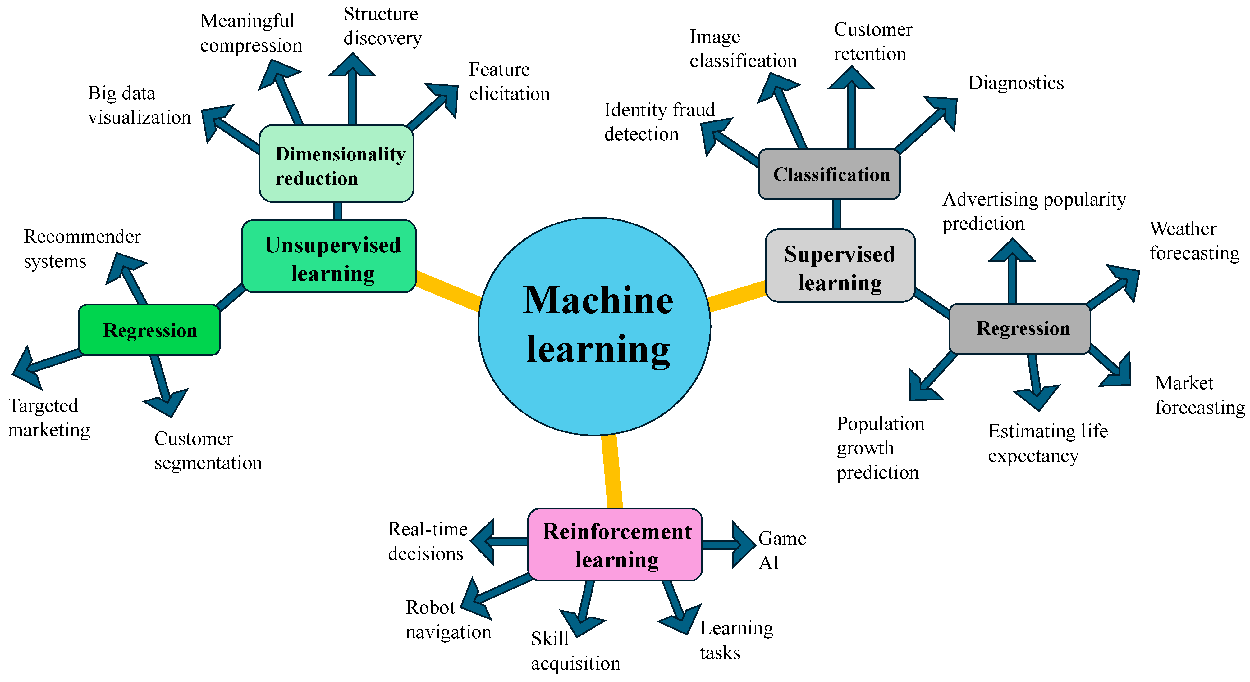
  163. Sarker, I.H. Machine Learning: Algorithms, Real-World Applications and Research Directions. SN Comput. Sci. 2021, 2, 160. [Google Scholar] [CrossRef]
  164. Gupta, V.; Mishra, V.K.; Singhal, P.; Kumar, A. An Overview of Supervised Machine Learning Algorithm. In Proceedings of the 2022 11th International Conference on System Modeling & Advancement in Research Trends (SMART), Moradabad, India, 16–17 December 2022; pp. 87–92. [Google Scholar] [CrossRef]
  165. Tchio, G.M.T.; Kenfack, J.; Kassegne, D.; Menga, F.-D.; Ouro-Djobo, S.S. A Comprehensive Review of Supervised Learning Algorithms for the Diagnosis of Photovoltaic Systems, Proposing a New Approach Using an Ensemble Learning Algorithm. Appl. Sci. 2024, 14, 2072. [Google Scholar] [CrossRef]
  166. Kaelbling, L.P.; Littman, M.L.; Moore, A.W. Reinforcement Learning: A Survey. J. Artif. Intell. Res. 1996, 4, 237–285. [Google Scholar] [CrossRef]
  167. Jin, Z.; Mei, S.; Chen, S.; Li, Y.; Zhang, C.; He, Y.; Yu, X.; Yu, C.; Yang, J.K.W.; Luk’yanchuk, B.; et al. Complex Inverse Design of Meta-optics by Segmented Hierarchical Evolutionary Algorithm. ACS Nano 2019, 13, 821–829. [Google Scholar] [CrossRef]
  168. Machine Learning and Evolutionary Algorithm Studies of Graphene Metamaterials for Optimized Plasmon-Induced Transparency. Available online: https://opg.optica.org/oe/fulltext.cfm?uri=oe-28-13-18899&id=432535 (accessed on 1 July 2024).
  169. Candeias, J.; de Araújo, D.R.; Miranda, P.; Bastos-Filho, C.J. Memetic evolutionary algorithms to design optical networks with a local search that improves diversity. Expert Syst. Appl. 2023, 232, 120805. [Google Scholar] [CrossRef]
  170. Phase-Controlled Metasurface Design via Optimized Genetic Algorithm. Available online: https://www.degruyter.com/document/doi/10.1515/nanoph-2020-0132/html (accessed on 1 July 2024).
  171. An, S.; Zheng, B.; Shalaginov, M.Y.; Tang, H.; Li, H.; Zhou, L.; Ding, J.; Agarwal, A.M.; Rivero-Baleine, C.; Kang, M.; et al. Deep learning modeling approach for metasurfaces with high degrees of freedom. Opt. Express 2020, 28, 31932–31942. [Google Scholar] [CrossRef] [PubMed]
  172. Lin, A. A Meta-Learning Reinforcement Training Method for Machine Learning Image-to-Image Optical Proximity Correction. Engineering Archive. Available online: https://engrxiv.org/preprint/view/3197/version/4499 (accessed on 1 July 2024).
  173. Zhang, D.; Qin, F.; Zhang, Q.; Liu, Z.; Wei, G.; Xiao, J.J. Segmented Bayesian optimization of meta-gratings for sub-wavelength light focusing. J. Opt. Soc. Am. B 2020, 37, 181–187. [Google Scholar] [CrossRef]
  174. Sun, M.; Kovanis, V.; Lončar, M.; Lin, Z. Bayesian optimization of Fisher Information in nonlinear multiresonant quantum photonics gyroscopes. Nanophotonics 2024, 13, 2401–2416. [Google Scholar] [CrossRef]
  175. Abu, M.; Zahri, N.A.H.; Amir, A.; Ismail, M.I.; Yaakub, A.; Fukumoto, F.; Suzuki, Y. Analysis of the Effectiveness of Metaheuristic Methods on Bayesian Optimization in the Classification of Visual Field Defects. Diagnostics 2023, 13, 1946. [Google Scholar] [CrossRef]
  176. Tunio, M.H.; Li, J.P.; Zeng, X.; Akhtar, F.; Shah, S.A.; Ahmed, A.; Yang, Y.; Bin Heyat, B. Meta-knowledge guided Bayesian optimization framework for robust crop yield estimation. J. King Saud Univ.-Comput. Inf. Sci. 2024, 36, 101895. [Google Scholar] [CrossRef]
  177. Schneider, P.-I.; Santiago, X.G.; Soltwisch, V.; Hammerschmidt, M.; Burger, S.; Rockstuhl, C. Benchmarking Five Global Optimization Approaches for Nano-optical Shape Optimization and Parameter Reconstruction. ACS Photonics 2019, 6, 2726–2733. [Google Scholar] [CrossRef]
  178. Ji, W.; Chang, J.; Xu, H.-X.; Gao, J.R.; Gröblacher, S.; Urbach, H.P.; Adam, A.J.L. Recent advances in metasurface design and quantum optics applications with machine learning, physics-informed neural networks, and topology optimization methods. Light Sci. Appl. 2023, 12, 169. [Google Scholar] [CrossRef]
  179. Elsawy, M.M.R.; Lanteri, S.; Duvigneau, R.; Brière, G.; Mohamed, M.S.; Genevet, P. Global optimization of metasurface designs using statistical learning methods. Sci. Rep. 2019, 9, 17918. [Google Scholar] [CrossRef]
  180. Hosna, A.; Merry, E.; Gyalmo, J.; Alom, Z.; Aung, Z.; Azim, M.A. Transfer learning: A friendly introduction. J. Big Data 2022, 9, 102. [Google Scholar] [CrossRef]
  181. Weiss, K.; Khoshgoftaar, T.M.; Wang, D.D. A survey of transfer learning. J. Big Data 2016, 3, 1345–1459. [Google Scholar] [CrossRef]
  182. Xu, D.; Luo, Y.; Luo, J.; Pu, M.; Zhang, Y.; Ha, Y.; Luo, X. Efficient design of a dielectric metasurface with transfer learning and genetic algorithm. Opt. Mater. Express 2021, 11, 1852–1862. [Google Scholar] [CrossRef]
  183. Huisman, M.; Plaat, A.; van Rijn, J.N. Understanding transfer learning and gradient-based meta-learning techniques. Mach. Learn. 2023, 113, 4113–4132. [Google Scholar] [CrossRef]
  184. Peng, R.; Ren, S.; Malof, J.; Padilla, W.J. Transfer learning for metamaterial design and simulation. Nanophotonics 2024, 13, 2323–2334. [Google Scholar] [CrossRef]
  185. Lv, J.; Zhang, R.; Gu, Q.; Uddin, H.; Jiang, X.; Qi, J.; Si, G.; Ou, Q. Metasurfaces and their intelligent advances. Mater. Des. 2023, 237, 112610. [Google Scholar] [CrossRef]
  186. Jia, Y.; Qian, C.; Fan, Z.; Cai, T.; Li, E.-P.; Chen, H. A knowledge-inherited learning for intelligent metasurface design and assembly. Light Sci. Appl. 2023, 12, 82. [Google Scholar] [CrossRef]
  187. Fan, Z.; Qian, C.; Jia, Y.; Chen, M.; Zhang, J.; Cui, X.; Li, E.-P.; Zheng, B.; Cai, T.; Chen, H. Transfer-Learning-Assisted Inverse Metasurface Design for 30% Data Savings. Phys. Rev. Appl. 2022, 18, 024022. [Google Scholar] [CrossRef]
  188. Cockerham, A.; Horton, C.; Kuebler, S.M.; Touma, J. Using AI-Assisted Inverse Design for Metalens Performance Optimization. In Proceedings of the 2023 IEEE Research and Applications of Photonics in Defense Conference (RAPID), Miramar Beach, FL, USA, 11–13 September 2023; pp. 1–2. [Google Scholar] [CrossRef]
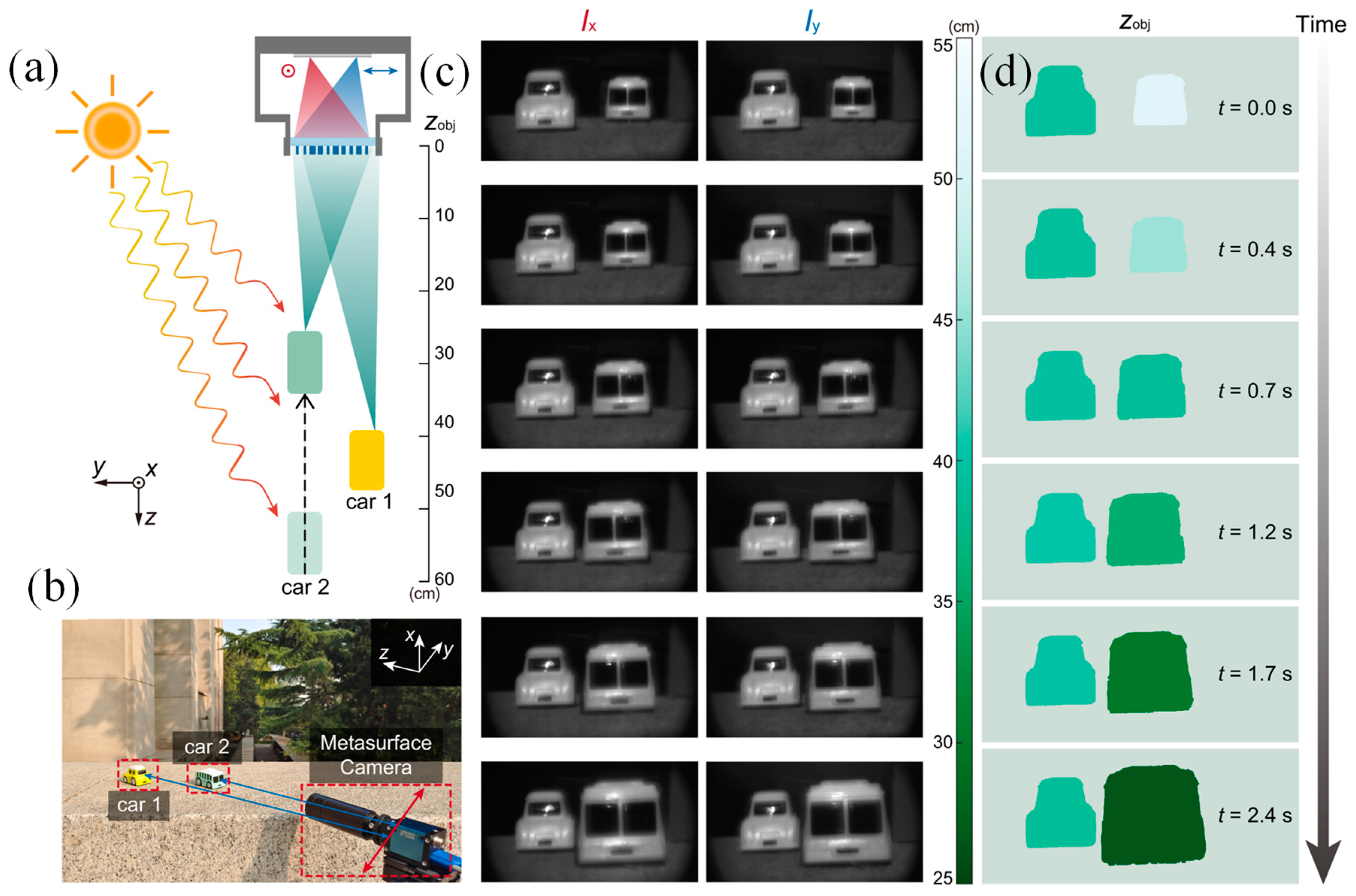
  189. Shen, Z.; Zhao, F.; Jin, C.; Wang, S.; Cao, L.; Yang, Y. Monocular metasurface camera for passive single-shot 4D imaging. Nat. Commun. 2023, 14, 1035. [Google Scholar] [CrossRef]
  190. Zhang, Y.; Wu, Y.; Huang, C.; Zhou, Z.-W.; Li, M.; Zhang, Z.; Chen, J. Deep-learning enhanced high-quality imaging in metalens-integrated camera. Opt. Lett. 2024, 49, 2853–2856. [Google Scholar] [CrossRef]
  191. Colburn, S.; Zhan, A.; Majumdar, A. Metasurface optics for full-color computational imaging. Sci. Adv. 2018, 4, eaar2114. [Google Scholar] [CrossRef]
  192. Yang, J.; Cui, K.; Cai, X.; Xiong, J.; Zhu, H.; Rao, S.; Xu, S.; Huang, Y.; Liu, F.; Feng, X.; et al. Ultraspectral Imaging Based on Metasurfaces with Freeform Shaped Meta-Atoms. Laser Photonics Rev. 2022, 16, 2100663. [Google Scholar] [CrossRef]
  193. Hsu, W.-L.; Huang, C.-F.; Tan, C.-C.; Liu, N.Y.-C.; Chu, C.H.; Huang, P.-S.; Wu, P.C.; Yiin, S.J.; Tanaka, T.; Weng, C.-J.; et al. High-Resolution Metalens Imaging with Sequential Artificial Intelligence Models. Nano Lett. 2023, 23, 11614–11620. [Google Scholar] [CrossRef] [PubMed]
  194. Wang, N.; Yan, W.; Qu, Y.; Ma, S.; Li, S.Z.; Qiu, M. Intelligent designs in nanophotonics: From optimization towards inverse creation. PhotoniX 2021, 2, 22. [Google Scholar] [CrossRef]
  195. Alagappan, G.; Ong, J.R.; Yang, Z.; Ang, T.Y.L.; Zhao, W.; Jiang, Y.; Zhang, W.; Png, C.E. Leveraging AI in Photonics and Beyond. Photonics 2022, 9, 75. [Google Scholar] [CrossRef]
  196. Liu, X.; Chen, M.K.; Tsai, D.P. Photonic Meta-Neurons. Laser Photonics Rev. 2024, 18, 2300456. [Google Scholar] [CrossRef]
  197. Wright, L.G.; Onodera, T.; Stein, M.M.; Wang, T.; Schachter, D.T.; Hu, Z. Deep physical neural networks trained with backpropagation. Nature 2022, 601, 549–555. [Google Scholar] [CrossRef]
  198. Zhelyeznyakov, M.; Fröch, J.; Wirth-Singh, A.; Noh, J.; Rho, J.; Brunton, S.; Majumdar, A. Large area optimization of meta-lens via data-free machine learning. Commun. Eng. 2023, 2, 60. [Google Scholar] [CrossRef]
  199. Khonina, S.; Kazanskiy, N.; Efimov, A.; Nikonorov, A.; Oseledets, I.; Skidanov, R.; Butt, M. A perspective on the artificial intelligence’s transformative role in advancing diffractive optics. iScience 2024, 27, 110270. [Google Scholar] [CrossRef]
  200. Optical Transformers|OpenReview. Available online: https://openreview.net/forum?id=Xxw0edFFQC (accessed on 18 July 2024).
Figure 1. Schematic illustration of (a) bulky refractive lens [72], (b) diffractive lens [72], (c) metalens [72].
Technologies 12 00143 g001
Figure 3. Types of ML: USL, SL and reinforcement learning.
Technologies 12 00143 g003
Figure 4. (a,b) Graphical illustration and photograph of the outdoor scene used for the dynamic imaging experiment under sunlight. In this setup, Car 2 moves towards the MS camera at a non-uniform speed of approximately 10 cm/s, while Car 1 remains stationary [189]; (c) the decoded all-in-focus polarization image pairs lx and ly of the scene for selected video frames [189]; (d) the retrieved depth maps for those frames from the recorded video [189].
Technologies 12 00143 g004
Figure 5. Images were captured under white light illumination of various subjects, including color-printed RGB (a) and ROYGBIV (b) text, a rainbow pattern (c), and a landscape scene (d) featuring a blue sky, green leaves, and multicolored flowers. The original, appropriately cropped object patterns used for imaging are displayed in the left column [191].
Technologies 12 00143 g005
Figure 6. The proposed ultraspectral imager is illustrated as follows [192]: (a) The imager is composed of three layers: an MS layer, a microlens layer, and an image sensor layer. SEM images of three such patterns are displayed on the right; (b) an optical micrograph shows the fabricated array of 20 × 20 different MS units, each measuring 17.58 µm × 17.58 µm and covering 3 × 3 pixels of a CMOS image sensor [192]; (c) this section displays the transmission spectra and effective indices of the Bloch modes for four MS units with freeform-shaped meta-atoms, highlighting their distinctive spectral characteristics [192]; (d) the generation process of the freeform-shaped patterns is detailed here: (i) a fine grid is generated; (ii) grid values are randomly assigned; (iii,iv) a blurring filter and thresholding function are applied in the first binarization process; (v,vi) a second binarization process further refines the patterns, smoothing edges and eliminating small features for feasible fabrication [192].
Technologies 12 00143 g006
Figure 7. (a) Representation of the VR near-eye projection system featuring an RGB-achromatic MO eyepiece paired with a laser-lit micro-LCD; (b) photograph of the optical setup corresponding to the red dashed line in (a) [6]. The micro-LCD is positioned on a motorized stage in front of the flat MOs [6]; (c) binary VR image displaying the Harvard logo in red, with a scale bar of 100 µm [6]; (d) zoomed-in aspect of the dashed area in (c), demonstrating that the MOs resolves individual pixels of the micro-LCD; (e,f) binary VR images of the MIT logo in green and blue, respectively [6]; (g,h) grayscale VR images of a building and a statue on the Harvard campus in red; (i,j) grayscale VR images of a Boston building and a lighthouse in green and blue, respectively [6].
Technologies 12 00143 g007
Table 1. Transformative role of AI in MOs.
BenefitDescriptionAI Techniques Involved
Design optimizationAI can optimize the design parameters of meta-optical components to achieve desired properties, such as minimizing aberrations or enhancing resolution.Machine learning (ML), Genetic algorithms (GAs) [38]
Inverse designAI algorithms can assist in the inverse design process, where desired optical responses are specified, and the system computes the necessary meta-structure to achieve these responses.Deep learning (DL), Neural networks [42]
Performance predictionAI can predict the performance of meta-optical devices under various conditions, reducing the need for extensive simulations and experimental trials.Predictive modeling, Regression analysis [43]
Material discoveryAI can help discover new materials with specific properties suitable for MOs applications by analyzing large datasets of material properties.Data mining, Bayesian optimization (BO) [44]
Fabrication process optimizationAI can optimize the fabrication processes of meta-optical components, improving yield and reducing defects.Reinforcement learning (RL), Process control algorithms [45]
Real-time adaptive opticsAI can enable real-time adjustments and corrections in adaptive optical systems, improving image quality and system performance in dynamic environments.Real-time data processing, Adaptive algorithms [46]
Pattern recognition and classificationAI can enhance pattern recognition and classification in imaging systems, improving the accuracy of optical sensing and imaging applications.Computer vision, convolutional neural networks [47]
Enhanced sensingAI can enhance the capabilities of meta-optical sensors by improving signal processing and noise reduction, leading to more accurate and reliable measurements.Signal processing, Noise reduction techniques [48]
Automated data analysisAI can automate the analysis of large datasets generated by meta-optical systems, extracting meaningful insights and reducing the need for manual analysis.Big data analytics, Automated feature extraction [49]
Virtual prototypingAI can create virtual prototypes of meta-optical devices, allowing for extensive testing and optimization before physical prototypes are built.Simulation, Virtual reality techniques [50]
Performance predictionAI can predict the performance of meta-optical devices under various conditions, reducing the need for extensive simulations and experimental trials.Predictive modeling, Regression analysis [51]
Table 2. Specifications of refractive lens, diffractive lens and metalens.
CharacteristicRefractive LensDiffractive LensMetalens
Working mechanismBending of light rays through refractionDiffraction and interferenceManipulation of light using nanostructures
MaterialTypically glass or plasticTypically plastic or glass with microstructuresDielectrics or metals with nanoscale structures
ThicknessGenerally thick, especially for high powerCan be very thinUltra-thin (sub-wavelength scale)
WeightRelatively heavyLighter compared to refractive lensesExtremely lightweight
AberrationsSusceptible to CAHigh CA but can be designed to minimize itCan be engineered to correct aberrations, including chromatic
Manufacturing ComplexityModerate to highHigh due to precise microstructure fabricationVery high due to nanoscale fabrication requirements
Focal Length VariationFixed for a given lens shapeFixed for a given structureCan be dynamically varied using external stimuli (e.g., voltage)
ApplicationsCommon in cameras, eyeglasses, microscopesUsed in diffractive optical elements (DOE), holographyAdvanced imaging systems, compact optical devices, AR
EfficiencyHighModerate (efficiency can decrease with diffraction orders)High efficiency can be achieved, but depends on design and material
ScalabilityScalable, but size affects weight and thicknessScalable with microfabrication techniquesHighly scalable with advanced nanofabrication techniques
Wavelength
Dependency
Less wavelength dependent (broadband)Strong wavelength dependenceCan be designed for specific wavelengths or broadband operation
Table 4. Characteristic table comparing various techniques in the field of AI and ML.
TechniqueDefinitionKey CharacteristicsApplications
MLAlgorithms that learn patterns from dataSL, USL, and semi-supervised learning. Focus on predictive accuracy. Requires labeled data for SLImage and speech recognition, predictive analytics, natural language processing
DLSubset of ML using NNsHierarchical learning architecture. Automated feature extraction. State-of-the-art performance in many domains. Requires large amounts of data and computational resourcesComputer vision, natural language processing, robotics
EAsOptimization techniques inspired by natural selectionPopulation-based optimization. Uses genetic operators (mutation, crossover). Suitable for complex, nonlinear problemsEngineering design, financial modeling, game-playing strategies
RLLearning through interaction with an environmentAgent learns by trial and error. Maximizes cumulative reward. Markov Decision Processes (MDPs) are often used as a frameworkGame playing (e.g., AlphaGo), robotics, Autonomous driving
BOOptimization technique based on BOUses prior information and observations to guide the search. Efficient for expensive, black-box functions. Balances exploration and exploitationHyperparameter tuning, experimental design, robotics motion planning
TLLeveraging knowledge from one domain for anotherTransfers knowledge learned from one task to improve learning in another task. Reduces the need for large amounts of labeled data in new domainsImage classification, natural language understanding, medical diagnosis
Disclaimer/Publisher’s Note: The statements, opinions and data contained in all publications are solely those of the individual author(s) and contributor(s) and not of MDPI and/or the editor(s). MDPI and/or the editor(s) disclaim responsibility for any injury to people or property resulting from any ideas, methods, instructions or products referred to in the content.

