Abstract
The optimization of DC-DC converters is crucial for enhancing their performance and efficiency in various applications. This study focuses on the sensitivity analysis of DC-DC converters to parametric variations, which plays a key role in designing robust and efficient systems. The methodology involves developing a simulation model that describes the behavior of converters under different conditions and analyzing the effects of parameter variations through simulation tools. Sensitivity analysis of DC-DC converters involves understanding the sources of harmonics, modeling the converter, analyzing the harmonic content, and implementing mitigation techniques. By combining theoretical analysis with practical design modifications, engineers can optimize DC-DC converters for improved performance, efficiency, and compliance with electromagnetic compatibility standards. Examples of harmonic analysis of the main types of DC-DC converters—Buck, Boost, and Buck-Boost—are discussed in the manuscript. Based on a study of the influence of harmonics in the operating modes, ratios have been derived to be applied during design. In this respect, the research presented is useful for designers and for use in power electronics education.
1. Introduction
Due to their ability to convert DC voltage from one level to another with maximum efficiency, DC-DC converters have a wide range of applications in various fields. Some of the main areas of use and specific examples of the application of DC-DC converters:
1. Electronics and communications: their main application is in the implementation of these components: chargers to convert the input voltage from the adapter to the voltage required to charge the battery; an internal power supply to manage various voltages for the processor, memory, and other components; and power modules in laptops and tablets, where they can maintain stable power for various systems and components, and optimize power consumption, thus extending battery life.
2. Industrial applications: in automation and control systems, they are used to provide a stable power supply for programmable logic controllers and other control devices, power various sensors and actuators in industrial systems, power robot components and automated systems, and to provide precise voltage control for various types of motors.
3. Renewable energy: in solar panels, they are used for the implementation of Maximum Power Point Tracking (MPPT), which are used to maximize and optimize the output power of solar panels, and for charge controllers that regulate the charging of batteries in solar systems; in wind generators, they are used to adjust the output voltage of the generators to ensure compatibility with the power grid or energy storage elements.
4. Automotive industry: they are used in inverters and converters for electric and hybrid vehicles, which are used to convert the voltage between the battery and the electric motor; on-board chargers that manage the charging of batteries from external sources; to power sensors and electronics, providing a stable voltage for various electronic systems in the car; and to support LED lighting and other lighting systems.
5. Medical equipment: they power various portable devices such as electrocardiographs, blood pressure monitors, and others, and provide reliable power for insulin pumps and other support devices; they also power stationary medical systems, such as MRI and CT scanners and other equipment that needs to provide a stable power supply for sensitive consumers.
6. Communication systems. they are used in power modules for routers and other communication devices and in mobile base stations for power management.
7. Aerospace technologies: they are used for the energy management of satellites and spacecrafts, where they provide reliable and efficient voltage conversions in solar panels and batteries; they are also in power management systems that regulate power for various systems and devices in spacecrafts.
DC-DC converters are indispensable in ensuring the quality of life of modern society, finding application in all fields of technology, because all devices need a power supply. In this sense, they provide reliable and efficient voltage conversion, which is critical for the proper operation of many devices and systems.
Power electronics sensitivity analysis is a process of evaluating the influence of various parameters and conditions on the operation of these devices. This analysis is important for the design and optimization of electronic systems to ensure their reliability and efficiency. The main steps and aspects related to this analysis are as follows:
1. Identification of critical parameters, which is carried out by determining the parameters that have the greatest influence on the operation of power electronic devices. These can be electrical parameters (voltage, current, power), temperature conditions, mechanical stresses, etc.
2. Development of a mathematical or simulation model that describes the behavior of the device. This includes the use of software such as SPICE, MATLAB/Simulink, and others.
3. Analysis of variations, which is realized by conducting simulations or experiments with variations of the selected parameters. This may include Monte Carlo simulations, parametric analyses, impact with variable frequency sources, etc.
4. Evaluation of the responses of the devices to the applied stressors. This includes analysis of parameters such as power output, efficiency, temperature profiles, and structural integrity.
5. Identification of critical conditions by determining the conditions under which the device exhibits the greatest sensitivity. This helps in optimization and design improvement.
The most commonly used tools for this type of analysis are SPICE Simulators (allow detailed analyses of electrical circuits and components); Monte Carlo simulations (used for statistical analysis of variations and their influence); Finite Element (FEM) analyses (used to analyze thermal and mechanical effects; and MATLAB/Simulink (offers flexibility for modeling simulations of complex systems).
In the present work, an analysis of the sensitivity of basic circuits of DC-DC converters will be presented by injecting harmonics into one of the nodes of the circuit and evaluating the impact of these harmonics on the others. In this sense, the analysis of the sensitivity of power electronic devices by injection of harmonics is a method of assessing the stability of these devices without the presence of a controller (a control circuit for regulating the output). This analysis is important for understanding the behavior of devices in real operating conditions, where they are subjected to various disturbances with a wide frequency spectrum, and for guaranteeing their performance.
2. Literature Review
The design of DC-DC converters includes many methods and techniques that ensure efficient and stable operation of the device. These methods cover various aspects such as topology selection, control, filtering and thermal management. Currently, applied methods for designing DC-DC converters include the following basic steps [1,2,3]:
1. Topology selection. For example, the main topologies that are discussed in the manuscript are: Buck converter, which is used to step down the voltage; Boost converter, which is applied when it is necessary to increase the output voltage relative to the input; a Buck-Boost converter that can both step down and step up the output voltage relative to the input. The main components of all three considered circuits are the same: transistor (MOSFET), diode/transistor, inductance, and capacitor. Of course, galvanically separated topologies such as Cuk, Sepik and Zeta are also used, which contain two transistors, two diodes, two inductors, and two capacitors, and allow both voltage scaling and voltage scaling with minimal current ripple and tension.
2. Simulation and modeling. Through the means of mathematical modeling, the behavior of the converter is described using a system of differential equations regarding the state variables. A simulation and analysis model is then created on this basis. The most commonly used simulation tools for this purpose are: LTspice, PSpice, MATLAB/Simulink, Python, and, with their help, time and frequency analyses are able to be carried out. As a result, an evaluation of the performance of the converters under different conditions is obtained.
3. Synthesis of control. For this purpose, pulse-width modulation (PWM) is most often used, controlling the width of the pulses to control the semiconductor switches (transistors) to adjust the output voltage. This is an easy to implement and effective method. Typical methods for controlling DC-DC converters: Current Mode Control, which is based on measuring and regulating the current through the inductor and, as a result, improves the stability and dynamics of the converter, and Voltage Mode Control, in which the output voltage is regulated and stabilized by comparison with a set reference value. This is a simpler method but usually requires additional compensation to achieve stability.
4. Filtering. LC filters are used, which are a combination of an inductance and a capacitor to suppress the high-frequency ripples of the currents and voltages in the circuit. A basic method of filtering in DC-DC converters uses a combination of two capacitors and one inductance for enhanced filtering -(π-filters). In this way, high frequency noise is reduced, and the quality of the output signal is improved.
5. Thermal management. Different types of heatsinks and fans are applied to effectively dissipate the heat generated by powerful components such as MOSFETs and diodes and, with their help, this keeps the operating temperature within acceptable limits. In addition, thermally conductive pastes and pads further improve thermal conductivity between components and cooling radiators, thus reducing thermal resistance.
6. EMI/EMC management. By using metal shields to reduce electromagnetic interference, both the converter itself and the surrounding electronic devices are protected. The inclusion of input and output filters to reduce EMI ensures compliance with electromagnetic compatibility (EMC) standards [4].
An example design process for a DC-DC converter from 12 V to 5 V is as follows: Topology selection: Select a Buck converter to step down the voltage from 12 V to 5 V; Simulation: Use LTspice to simulate the circuit and verify stability and performance. Control: Select a PWM controller to adjust the output voltage. Filtering: Enable an LC filter to suppress ripple in the output signal. Thermal Management: Mount a heatsink on the MOSFET to dissipate the heat generated. EMI/EMC management: Add an input and output filter to comply with electromagnetic compatibility standards.
The design of DC-DC converters requires the integration of multiple methods and techniques to achieve optimal performance, efficiency and reliability of the final device. In this sense, the design of DC-DC converters can be performed using various methods, each of which has its own advantages and disadvantages. The main methods of analysis are analytical, simulation, empirical, numerical, and modular. Table 1 compares the different analysis methods.

Table 1.
Comparative analysis of different methods for designing DC-DC converters.
The choice of design method for DC-DC converters depends on the specific project requirements, available resources, and desired accuracy. Often, the best approach is a combination of several methods, which gives a balanced solution, combining the advantages of each of them.
The design of DC-DC converters requires careful analysis of the harmonic components of the signal to ensure efficiency and minimize interference. Harmonic analysis helps to evaluate the unwanted frequencies generated by the converter and takes measures to suppress them. The following steps and techniques are used in the harmonic analysis of DC-DC converters:
1. Understanding the types of DC-DC converters, regarding their topology.
2. Modeling the converter with differential equations that describe the behavior of the circuit. Using simulation tools such as SPICE to analyze time and frequency characteristics.
3. Analysis of harmonics with Fourier analysis. Decomposing the signal into its constituent sinusoidal components. Spectrum Analysis: Using a spectrum analyzer to measure the harmonic components in the output signal.
4. Suppression of harmonics by filtering. Use of passive or active filters to suppress unwanted harmonic frequencies. PWM technique: Modification of pulse-width modulation to reduce harmonic distortions. EMI (Electromagnetic Interference): Using methods to suppress EMI, such as shielding and improving PCB (printed circuit board) design.
5. Measurements and optimization. Using an oscilloscope to measure voltages and currents in real time. Vector network analyzer: Measuring the frequency response of a converter. Parameter Optimization: Tuning converter parameters to minimize harmonic distortion and improve efficiency.
Harmonic analysis is a critical step in the design of DC-DC converters that ensures high efficiency and minimal interference. Through careful analysis and optimization, stable and efficient operation of the converter can be achieved.
By contrast, harmonic analysis is a widely used tool for studying stability in power electronics. The integration of decentralized power generation systems poses new challenges to the stability and power quality of modern power grids [5]. The stochastic nature of energy production and the associated power fluctuations cause harmonic instability to be introduced in the form of resonances or unusual harmonics over a wide frequency range. Harmonic stability is shown to be a variety of small-signal stability problems that contain waveform distortions at frequencies above and below the fundamental frequency of the system, and the role of harmonic stability analysis in ensuring the operability of large power transmission systems is argued. In this context, the influence of low-power electronic loads as one of the main sources of harmonic currents in distribution electrical networks is considered in [6]. A model of a typical low-power nonlinear electronic load is presented and its applicability to current harmonic calculations is demonstrated. Harmonic resonance and instability issues are of paramount importance in the development and integration of HVDC systems. In [7], the stability of a modular multilevel converter (MMC) was investigated by means of harmonic analysis. For this purpose, an impedance model of the MMC was used, and measures to improve the dynamics of the device were also proposed on this basis. Considering the impedance characteristics of DC transmission lines, the harmonic stability for the DC system is analyzed over a wide frequency range and a modified DC attenuation control is proposed based on this. In [8], a multi-harmonic model of single-inductor-double-output (SIDO) Buck DC-DC converters is presented to study the phenomenon of multiple harmonic oscillations and analyze the harmonics in different frequency domains. With the proposed model, multiple load-dependent harmonic oscillations have been identified and the distribution of the odd and even components of each harmonic has been obtained. A harmonic interaction index is introduced to estimate the degree of asymmetric waveform distortion in two adjacent half-waves. In this regard, the limits of the harmonic behavior of the system in the circuit parameter spaces are given to aid in optimal system design. In [9], a DC impedance model of a modular multilevel converter (MMC) is developed by the harmonic transfer function method, which takes into account the internal dynamics and operation of the controller. The internal dynamics are modulated based on the capacitor–voltage fluctuation and multi-harmonic response characteristics, and the control synthesis is performed with DC voltage control; phase current control based on positive–negative sequence separation; circulating current management; and others. As a result, the proposed impedance model provides information not only on the harmonic stability of the MMC, but also on the influence of the control synthesis on the system stability. Harmonic analysis is a powerful tool for the analysis and design of power converter topologies such as modular multilevel converters with passive circulating current filters (MMC-PCCF) [10]. Through proposed DC impedance models of MMC-PCCFs in different control modes, it is shown that more resonance points exist in these devices, leading to higher risks of harmonic instability. For a comprehensive study of system stability, a design-oriented harmonic stability analysis method is proposed. It is based on the sensitivity of the resistance and the sensitivity of the phase difference to the frequency, and the results obtained improve the stability of the system. In [11], a problem related to the harmonic analysis of a Buck converter with application in a system with Hall sensors was studied. A mathematical model of a step-down converter and its control system is presented and, based on Lyapunov’s theorem for ensuring the stability of the system, a new approach for determining the unmodeled dynamics of Hall sensors is proposed. From the research carried out, it can be concluded that the harmonic analysis and its inclusion in the design of power electronic converters to reduce losses in the converter and increase its efficiency are of great importance. In [12], a literature study of various types of multilevel converters for battery charging applications is presented. In the article, classic and innovative topologies for high-level application and strategies for implementing modulation for optimal distribution of energy flows during charge and discharge of batteries are discussed. In [13], a Zeta DC-DC converter is presented, for which a combined modeling and analysis approach is proposed, which includes the harmonic balance of the proposed scheme, as well as the small parameter equivalent method. Also, a comparison is made between classical methods for designing DC converters and the proposed new approach. From the simulation results, it is observed that the computer simulation time is significantly reduced and the changes of the state space ripples can be described more easily. In [14], a study of the influence of harmonic disturbances in the power system is performed. The main purpose of this study is to present and investigate the need to add additional filters to reduce the influence of harmonic components in the power system. In [15], a study of modular multilevel converters using harmonic state-space is presented. Modeling of small-signal converters was implemented and stability analysis was performed. From the results presented, it can be observed that the use of state space is a significant advantage in the design of different converter topologies.
From the analysis of the existing papers dedicated to the application of harmonic analysis in power electronics, the conclusion follows that it is widely used for the analysis and design of complex topologies and systems, but, at the same time, its application in relation to the classical topologies of DC-DC converters is highly limited. In this respect, the aim of the present work is to draw conclusions and recommendations related to their design based on models and the results of the harmonic analysis of the schemes of Buck, Boost, and Buck-Boost DC-DC converters.
3. Materials and Methods
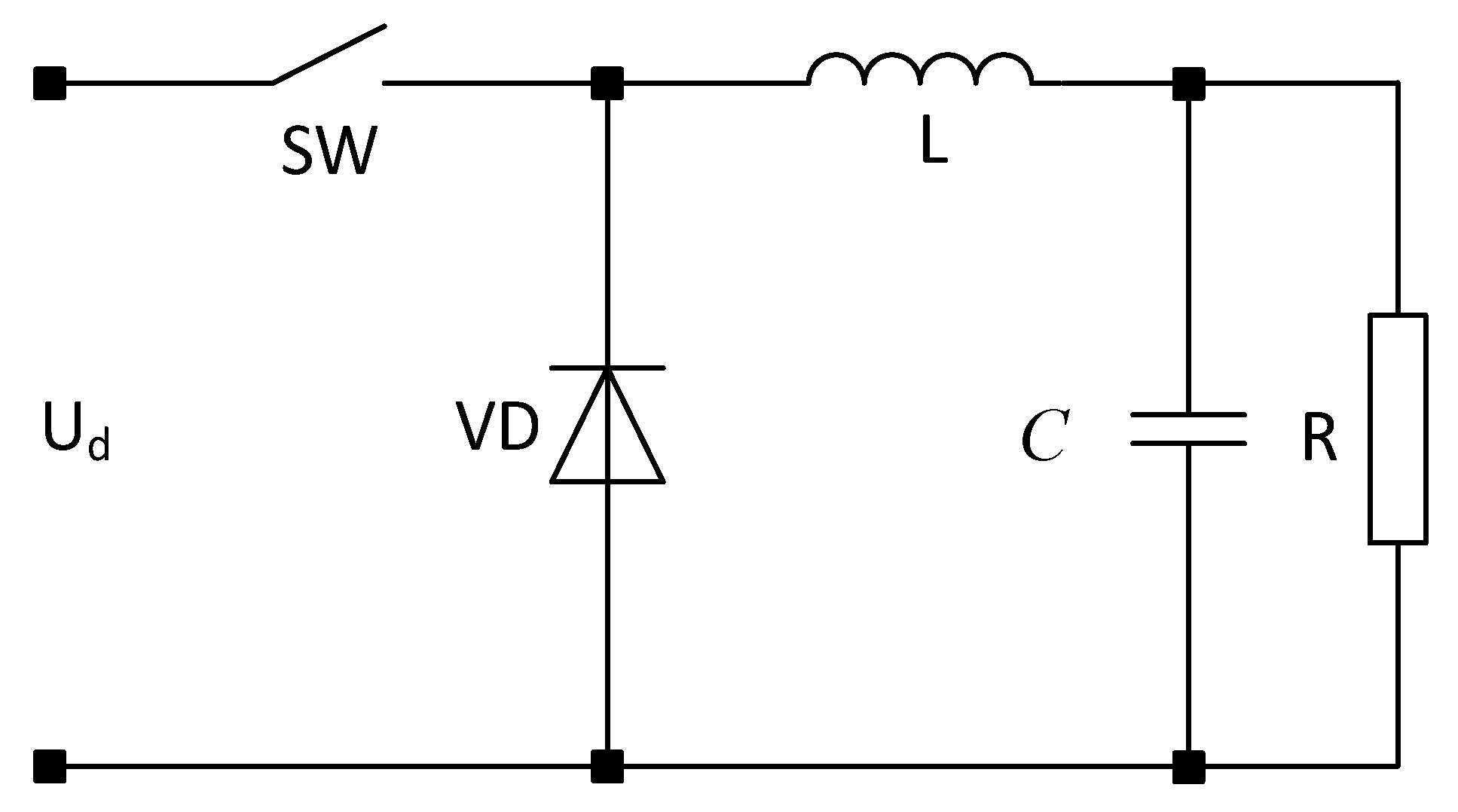
Based on the literature review on different types of DC-DC converters, a Buck converter is represented in Figure 1. It is used when it is necessary to lower the output voltage compared to the input voltage.

Figure 1.
Scheme of Buck DC-DC converter.
Descriptions of the operation modes of the Buck DC-DC converter use the following equations [16,17,18]:
The ratio between the input and output voltages can be represented after solving Equation (1):
where the following designations are used:
- Ud is the input voltage.
- Uo is the output voltage.
- UL is the voltage of the inductor L.
- D is the duty cycle.
- T is the period.
- ton is the period when the switch is on.
Based on the presented equations for the principle of operation of the converter, a state space is used, which is a multidimensional matrix with the coefficients that do not change during the calculations in the time domain. In this sense, the matrix A is a multidimensional matrix which is composed by the coefficients which do not have amendment during all the calculation in the time domain. The matrix B is the input vector matrix which defines the disturbing influences in the system. The designations used are presented in the mathematical model in MATLAB/Simulink:
where
- L1 is the input inductance.
- L2 is the internal inductance of the diode.
- C1 is the internal capacitance of the transistor.
- C2 is the capacitance of the output filter capacitor.
- C3 is the internal capacitance of the load.
- LL is the internal inductance of the load.
- R1 is the resistance of the load.
- r1 is the internal resistance of the inductance L1
- r2 is the internal resistance of the inductance L2
- C is filter capacitance.
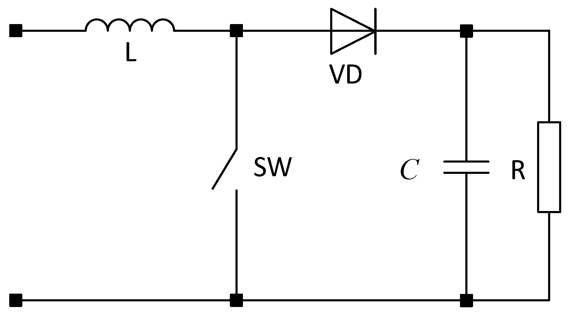
Another example of a DC-DC converter used in applications where we need to have a higher output voltage relative to the input is the boost converter. In its design, the same circuit elements are used, but the connection point of the transistor is different. The scheme is presented in Figure 2.
Figure 2.
Scheme of Boost DC-DC converter.
A Boost DC-DC converter is also called an inverting converter because the power source outputs power with the transistor off. The basic operation modes can be described by the following equations [10,19,20]:
After transformations in Equation (4), the following dependence for the ratio between input and output voltage can be derived:
Similarly, in the Boost DC-DC converter, a state space is used to describe the principle of operation of the circuit in matrix form. Similar notations are used.
In the present article, research has also been carried out on the inverting Buck-Boost DC-DC converter. Its circuit is shown in Figure 3. It is called inverting because the output voltage is of the opposite polarity to the input voltage.
Figure 3.
Scheme of Buck-Boost DC-DC converter.
Like the other presented converters, the principle of operation can be described by the following equations [21,22]:
After solving Equation (6), we can obtain the following ratio of input to output voltage:
The same designations are used for the other DC-DC converters. Specific to this converter is that, at different values of the duty cycle, the converter can operate in buck or boost mode. This is subject to the following duty cycle constraints:
Similar methodology for Buck-Boost DC-DC converter is used and the differential equation is presented in a matrix form.
4. Results
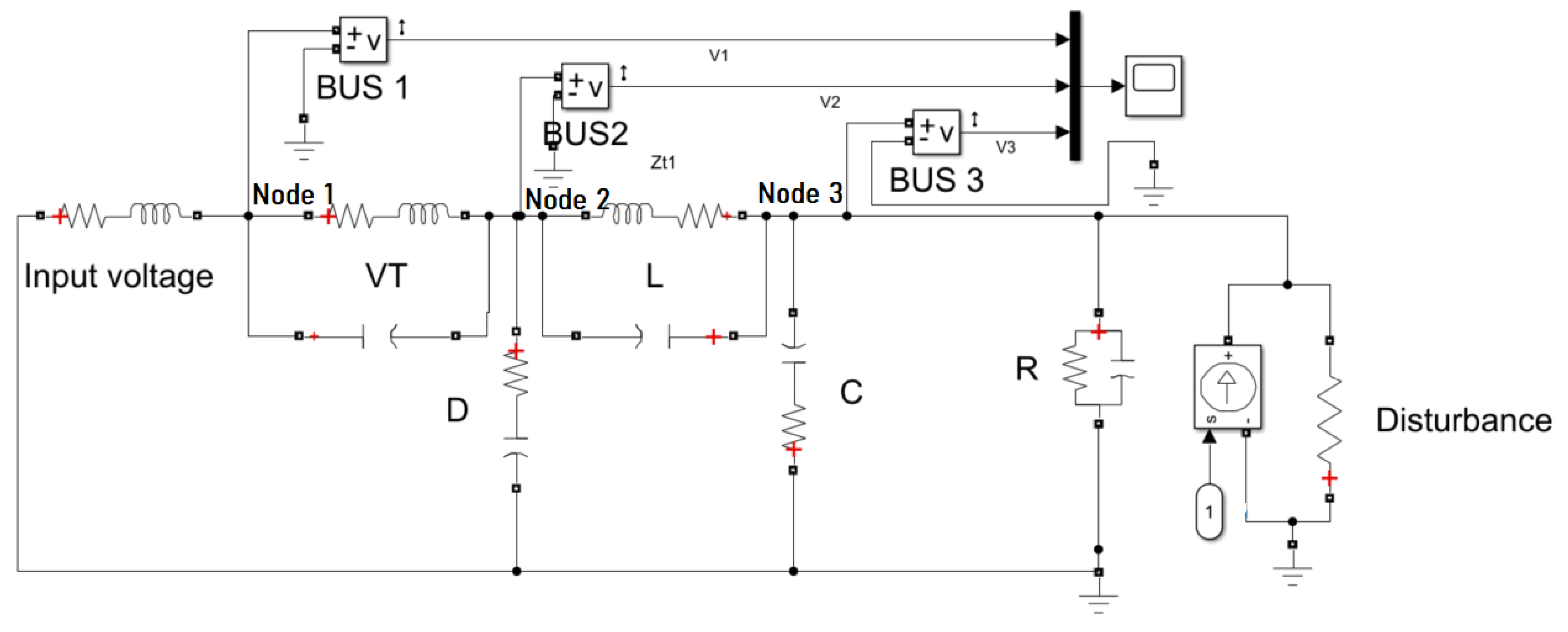
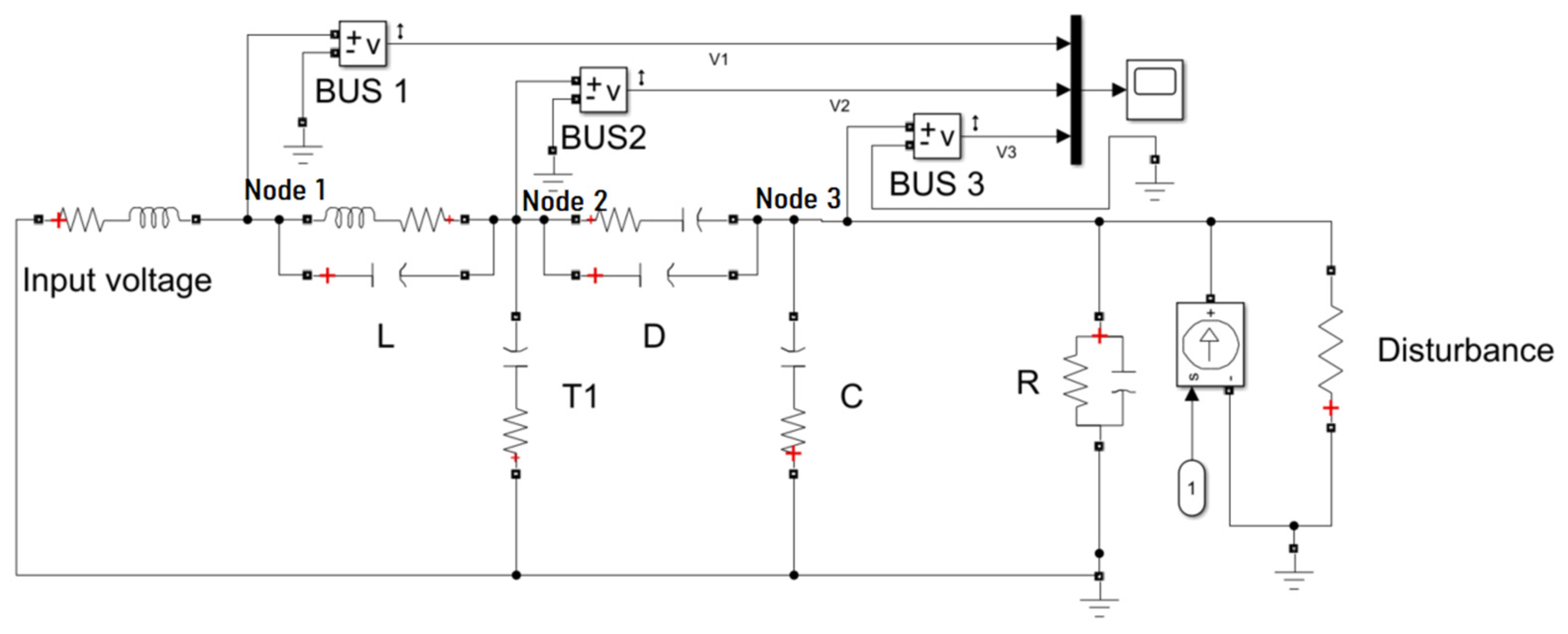
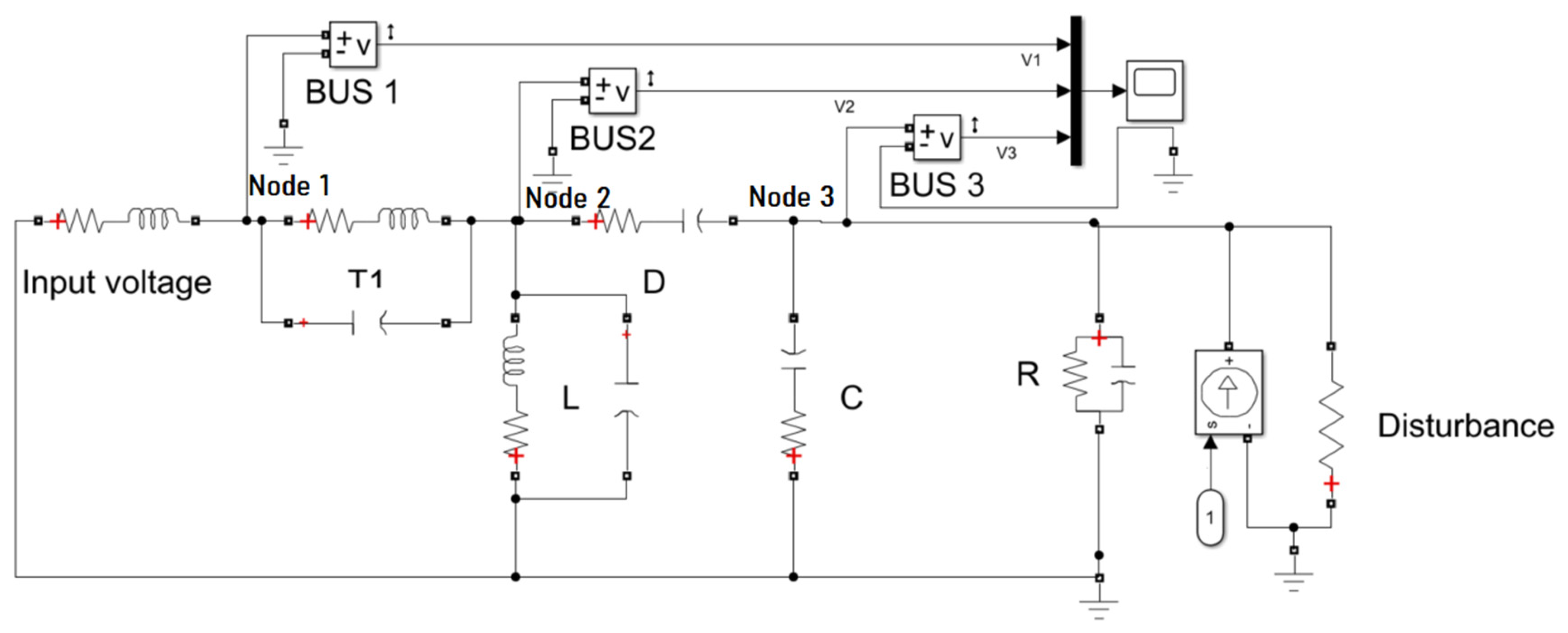
In this paper, several studies of DC-DC converters are realized. The simulation models were realized in MATLAB/Simulink. The initial values of the schematic elements were determined by standard methodology [23,24,25,26]. The input voltage was 24 V. The input DC voltage source was presented with the RL series circuit with a relatively low value of the inductance and the resistance. The transistor T1 was presented when the switch mode was in the time interval Ton. For better calculation process, a capacitor with a very small capacitance value was added in parallel to the transistor and the inductance L. In parallel with them, the diode was connected, which, in this time interval, does not conduct, to the output capacitor. Each of the circuit elements used was presented as an equivalent circuit using resistance and capacitor or resistance and inductance, depending on the nature of the specific element. Three voltmeters were connected to the “Scope” block, with the help of which the influence of injection of 1 per unit (p.u.) disturbing effect in Node 3. Bus 1 was observed on the scheme implemented in MATLAB/Simulink, similar to the other two nodes, bus 2 and bus 3. Only the perturbation injection at Node three can be observed in Figure 4. To perform the remaining simulation studies, respectively, the disturbance must be moved and injected first into Node 2, then into Node 1.

Figure 4.
Simulation scheme of Buck DC-DC converter in MATLAB/Simulink.
The purpose of this research is to determine the operating frequency at which it is possible for a resonance process to occur in the different types of DC-DC converters.
Figure 4 shows the simulation scheme of the Buck DC-DC converter. The model is presented with a replacement schematic that includes a simplified model of the circuit elements. The type of elements are specified in the schematic, including the internal resistance and capacitance of the components. This modeling approach is chosen to provide a more detailed explanation of the operation of the converter.
In order to study the influence of the injected harmonics on the other nodes of the circuit, it is necessary to use a suitable simulation model. In this respect, the parameters of the simulation model were chosen in order to obtain an idealized source with which to conduct the simulation studies, taking into account the non-idealities of the circuit elements and ensuring a stable and convergent numerical solution in the simulations.
The used parameters of the schematic elements are presented in Table 2. The real elements, such as input voltage source, diode, transistor, capacitor, and inductance, are presented with their equivalent scheme. The value of the capacitors connected in parallel to all elements are significantly low C = 1 × 10⁻¹² F. This capacitor was added for better convergence during the simulation. The value of all the elements was similar for all the converters.
Table 2.
Parameters of the mathematical model of Buck DC-DC converter.
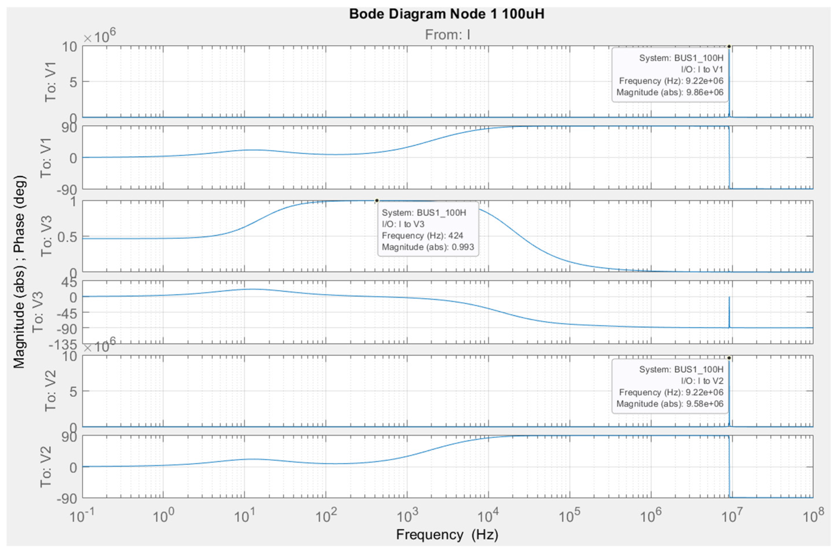
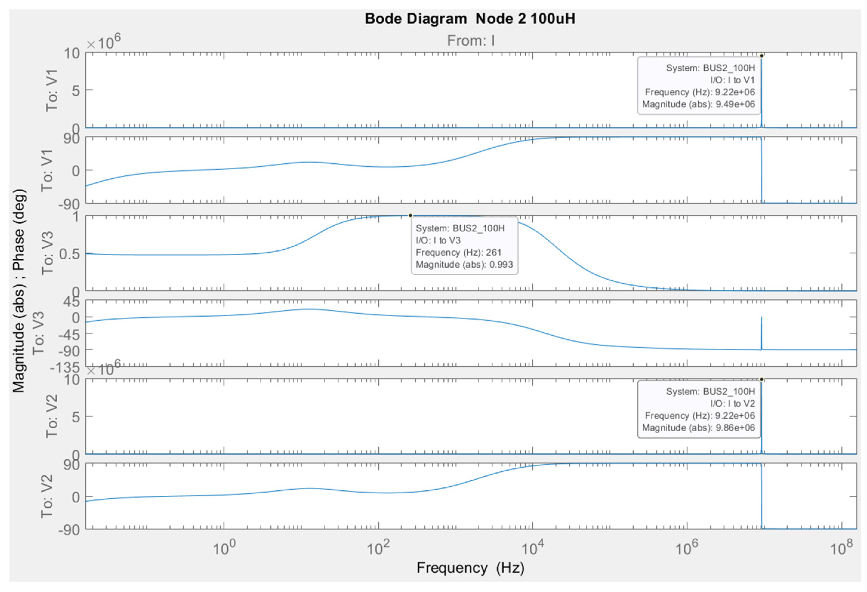
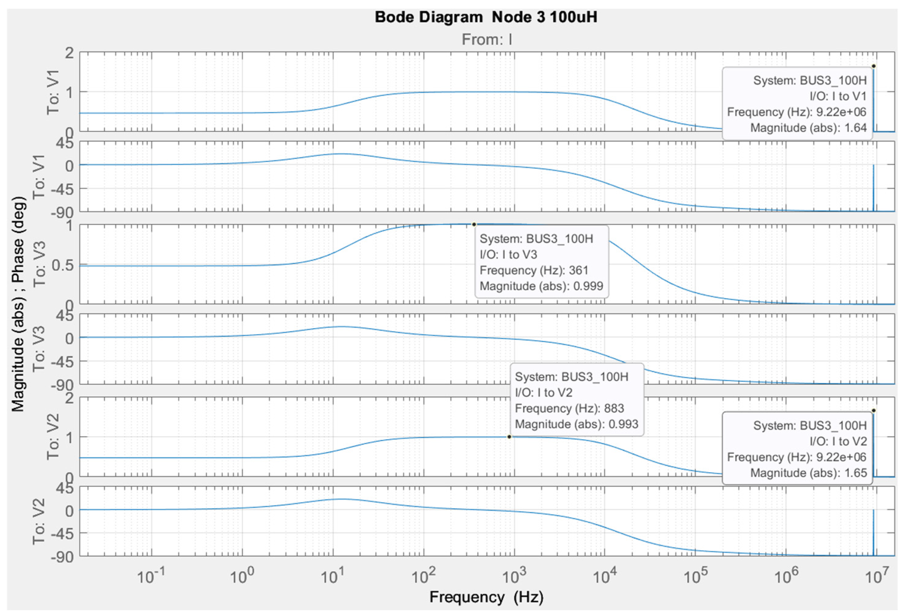
The following figures present the results of the simulation studies. Phase and magnitude curves of the studied scheme are presented. Several studies have been conducted at different inductance values. The switching frequency for all the studied converters was f = 100 kHz, duty cycle is D = 50%, the value of the load was R = 12 Ω. The initial value of the inductance was L = 100 µH. The value of the capacitance of the output capacitor was not changed and it was C = 5 µF for all the studies. The values of the internal inductance and resistance were standard and provided by the manufacturers. These are the same value for all the simulation studies. After that, several studies were performed to increase the value of inductance by 5, 10, and 15 times, while implementing a unit disturbance in each of the nodes of the circuit. From the simulation studies presented, the occurrence of resonance can be observed.
Figure 5 shows the change in phase and magnitude when implementing a unit disturbance in Node 1. The value of the inductance is L = 100 µH.
Figure 5.
Bode diagram for studying a Buck DC-DC converter, regarding Node 1 when L = 100 µH.
The graphs show the following: The magnitude responses of the system are almost constant up to a frequency of about 1 × 10⁶ Hz, after which we observe a slight decrease, indicating frequency limitations of the system. The phase responses show a significant phase drop at 4 Hz in the graphs for V1 and V2, which may signal resonance or phase changes at this frequency. Regarding V3, the phase remains almost unchanged, indicating phase stability of the system at most operating frequencies.
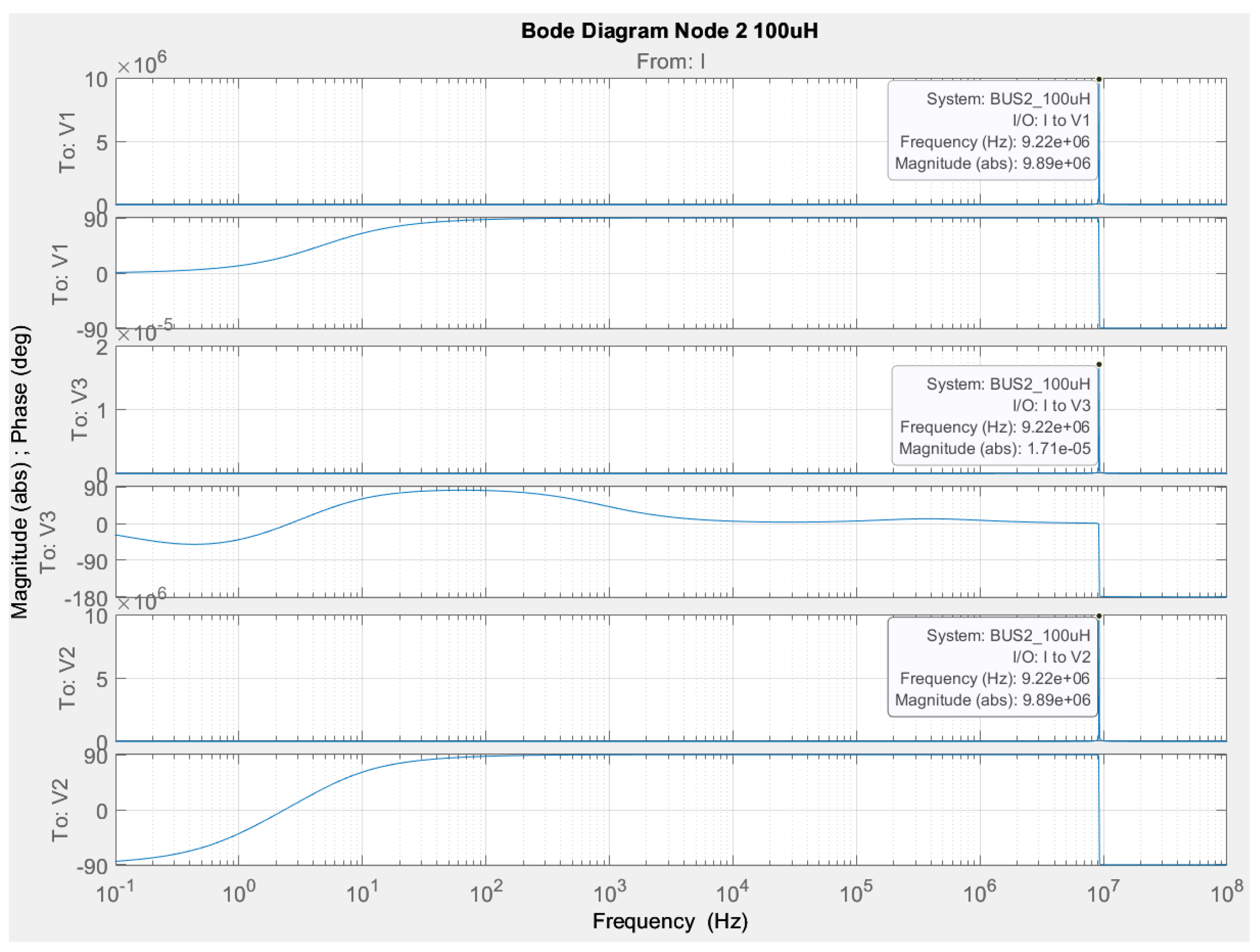
Figure 6 presents the simulation results of the implementation of a disruptive influence unit at Node 2. The inductance value is again L = 100 µH. The Bode plot shows six plots that represent the magnitude and phase responses of the system at different points. The magnitude responses show relative stability of the system with little or no change in amplitude up to very high frequencies (10 × 106 Hz), indicating good frequency response of the system. However, the phase responses show significant changes, reaching approximately −90 degrees, which may indicate the presence of resonance or phase transitions in the frequency range under study.
Figure 6.
Bode diagram for studying a Buck DC-DC converter, regarding Node 2 when L = 100 µH.
Figure 7 shows similar studies for Node 3. The plots show the following: The magnitude responses are relatively stable over the entire frequency range, with little or no change up to high frequencies, indicating that the system effectively maintains its amplitude response. The phase responses show more variation. The most notable feature is for V3, where there is a significant phase drop at a frequency of around 361 Hz. This sharp drop to −90 degrees could signal critical phase changes or potential resonance problems in this frequency range.
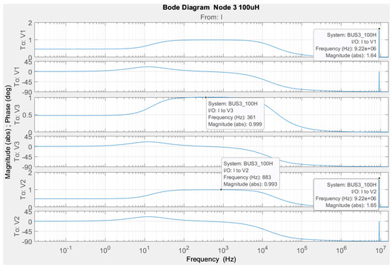
Figure 7.
Bode diagram for studying a Buck DC-DC converter, regarding Node 3 when L = 100 µH.
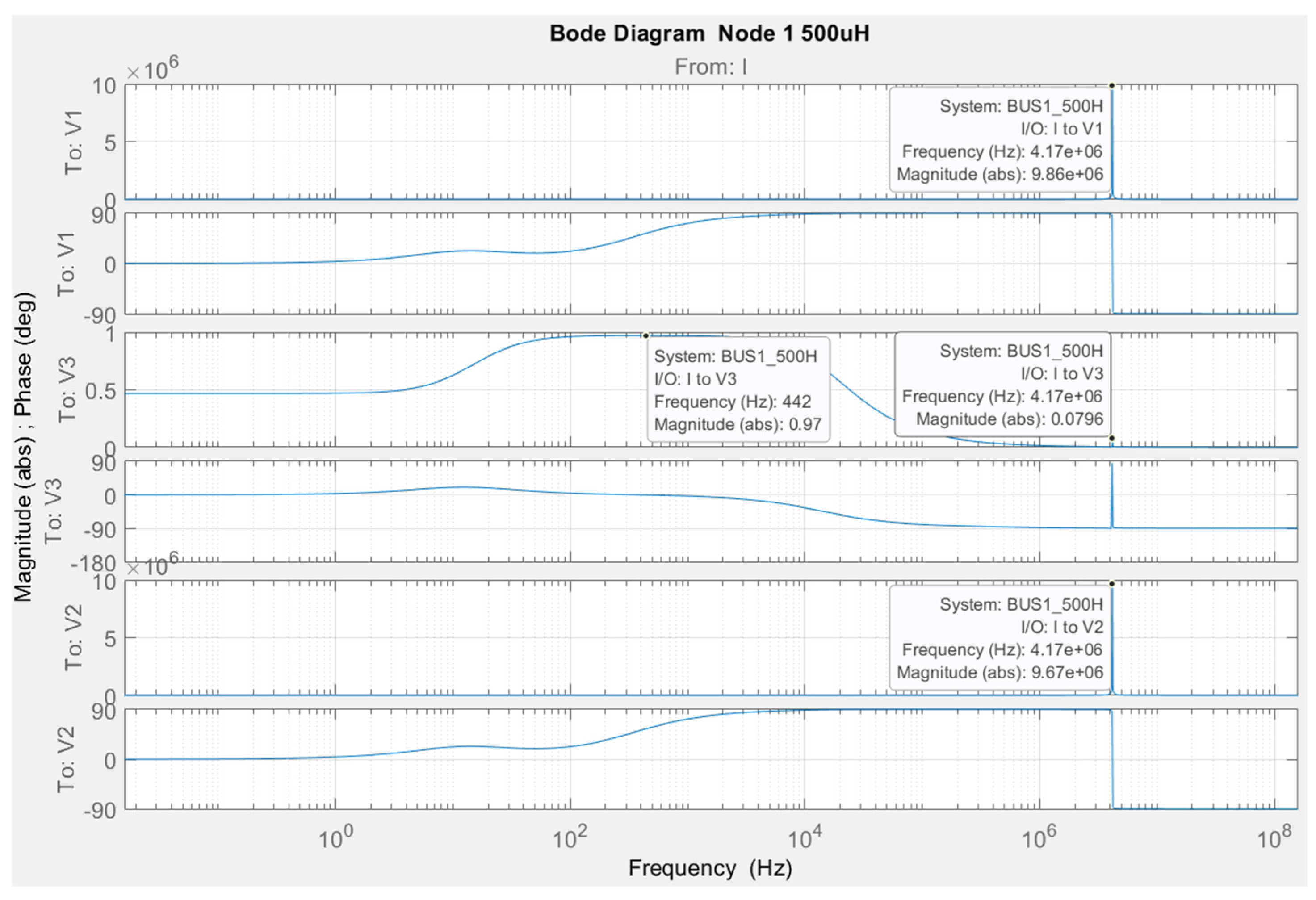
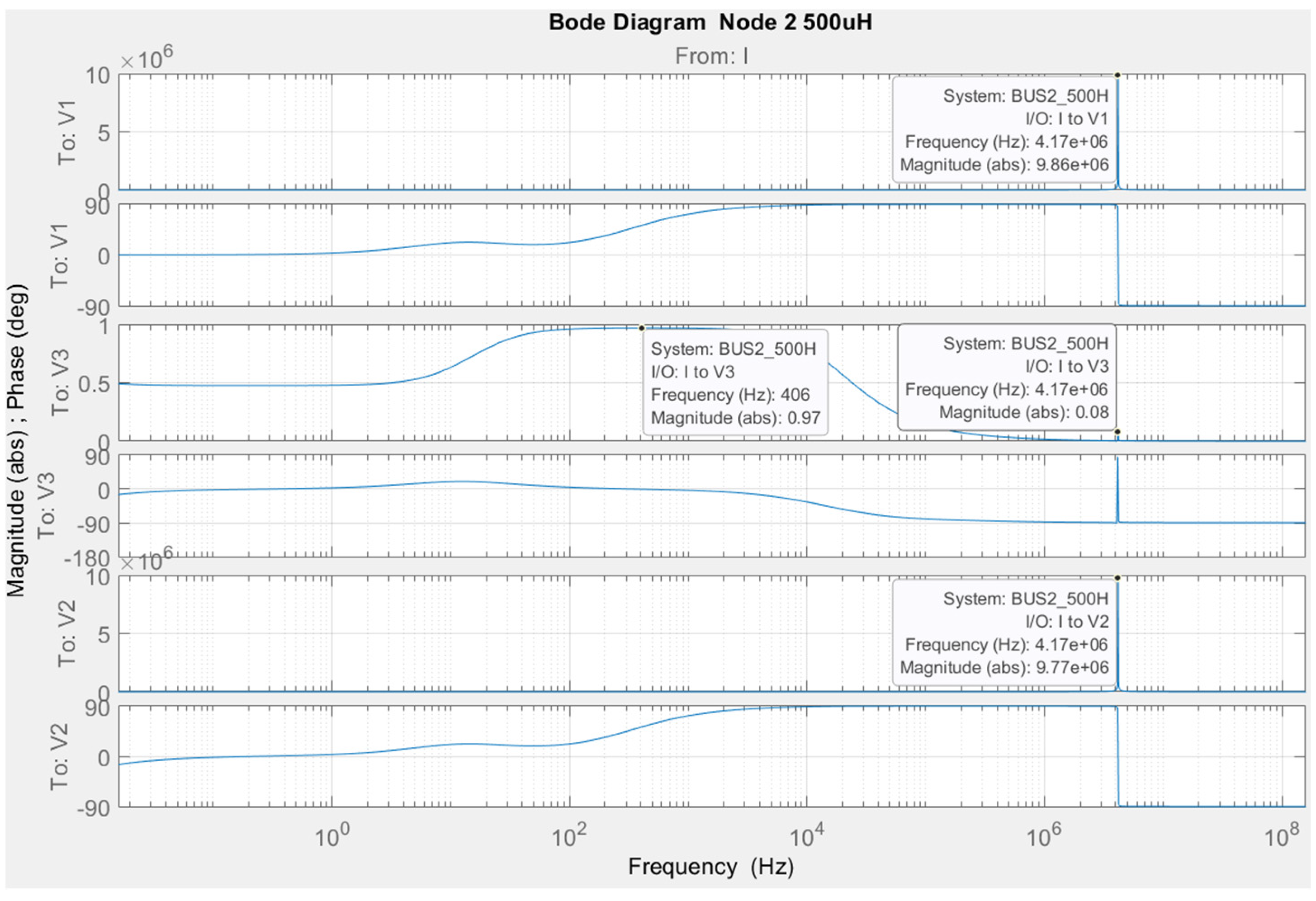
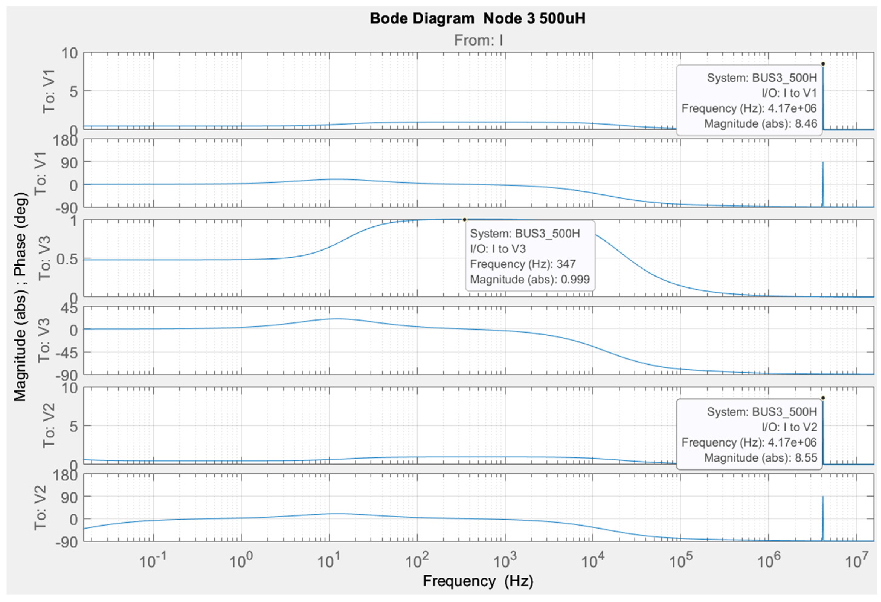
Simulation studies were also carried out when changing the filter inductance with a value five times higher than the initial one. Figure 8 shows the change in phase and magnitude when a disturbing effect is applied in Node 1. Similar studies were also carried out when a disturbing effect was implemented in Node 2 (Figure 9) and Node 3 (Figure 10).

Figure 8.
Bode diagram for studying a Buck DC-DC converter, regarding Node 1 when L = 500 µH.
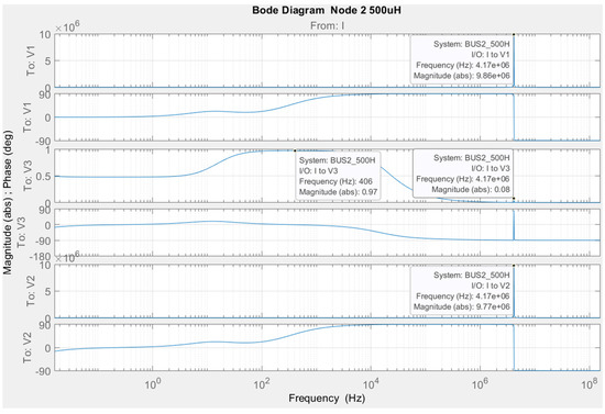
Figure 9.
Bode diagram for studying a Buck DC-DC converter, regarding Node 2 when L = 500 µH.
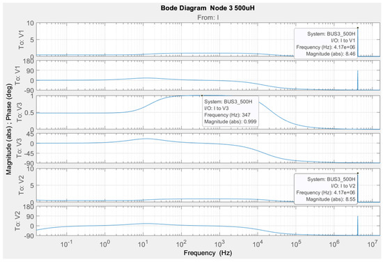
Figure 10.
Bode diagram for studying a Buck DC-DC converter, regarding Node 3 when L = 500 µH.
The Bode plot presented here shows six plots showing the magnitude and phase responses of the system at different frequencies, with the main conclusions being: The magnitude responses of the system are extremely stable over the entire frequency range up to about 1 × 10⁶ Hz, indicating that the system maintains its efficiency at different frequencies without significant changes in amplitude. The phase responses are variable, especially noticeable at about 442 Hz (relative to V3), where the phase drops sharply to −60 degrees, indicating potential resonance effects or phase instabilities at this frequency. In the other plots, the phase remains more stable, with small deviations.
The figure shows similar relationships as in previous studies, with the magnitude responses of the system being stable over most of the frequency range, with slight amplitude changes at high frequencies. This indicates that the system effectively maintains its functionality at different frequencies. The phase responses show some interesting changes. Again regarding V3, the phase drops sharply at around 406 Hz, reaching a significantly low level, which may indicate potential resonance or phase stability problems at this frequency.
The Bode plot presented in Figure 10 shows the magnitude and phase responses of the system at different frequencies, observing the following: The magnitude responses show high stability of the system with constant values up to very high frequencies, except for T0 V3, where a sharp drop is observed at 347 Hz, indicating a filter or resonance effect. The phase responses are mostly stable, except in cases where the magnitude responses show sharp changes. In such cases, the phases also show significant changes, highlighting the interaction between magnitude and phase at specific frequency characteristics.
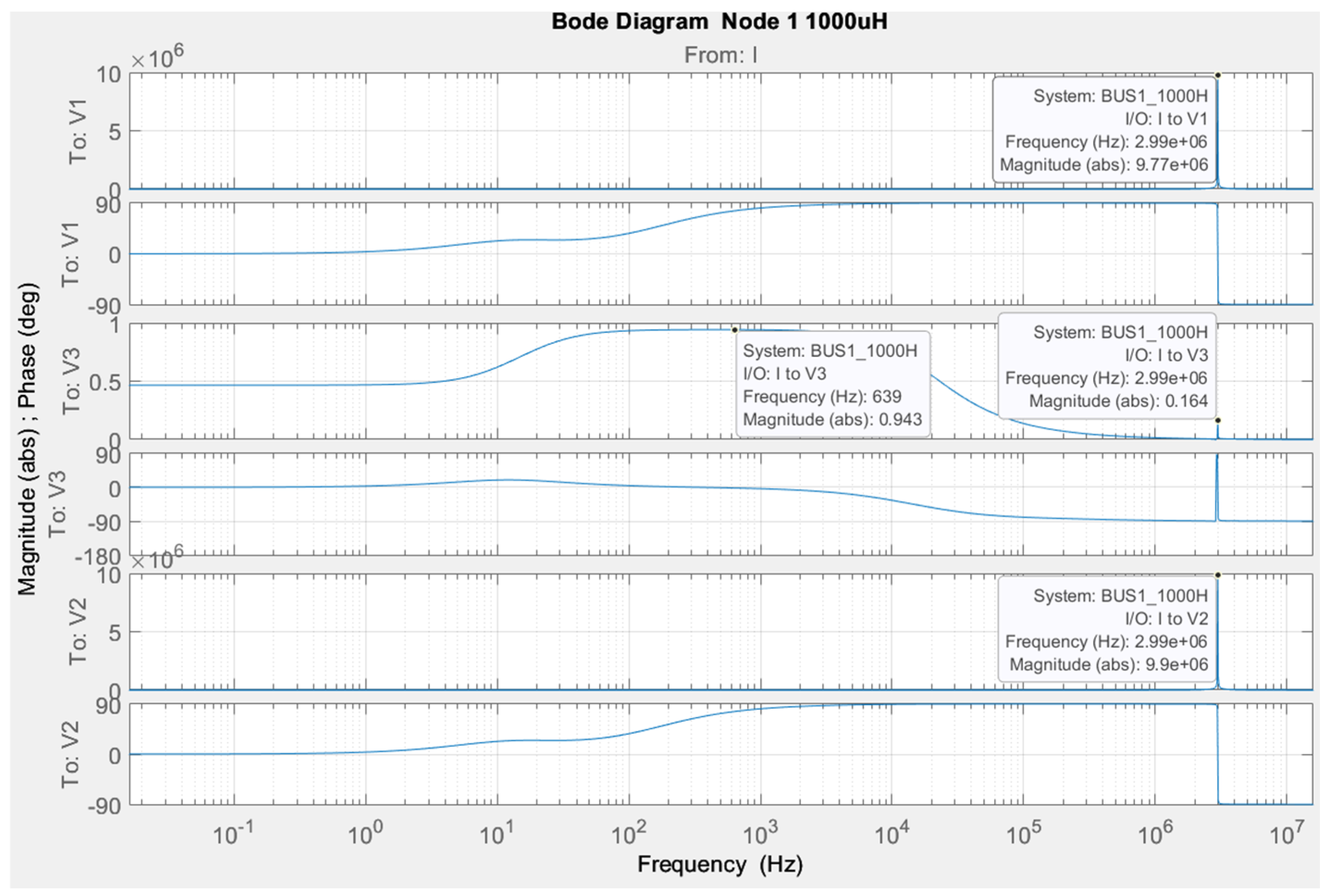
Figure 11, Figure 12 and Figure 13 present the simulation studies of the Buck DC-DC converter with filter inductance value L = 1000 µH.
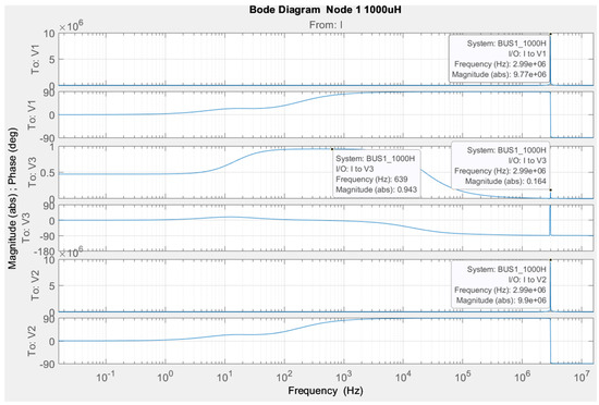
Figure 11.
Bode diagram for studying a Buck DC-DC converter, regarding Node 1 when L = 1 mH.
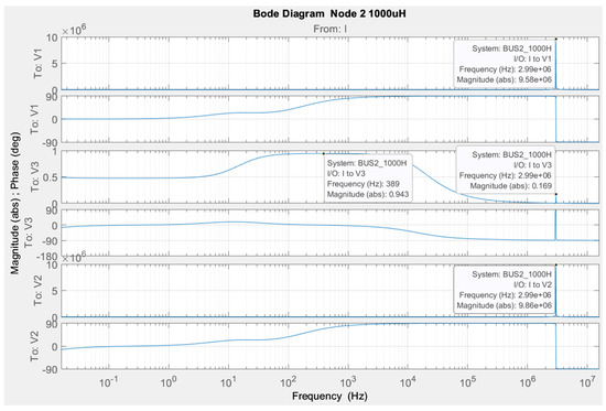
Figure 12.
Bode diagram for studying a Buck DC-DC converter, regarding Node 2 when L = 1 mH.

Figure 13.
Bode diagram for studying a Buck DC-DC converter, regarding Node 3 when L = 1 mH.
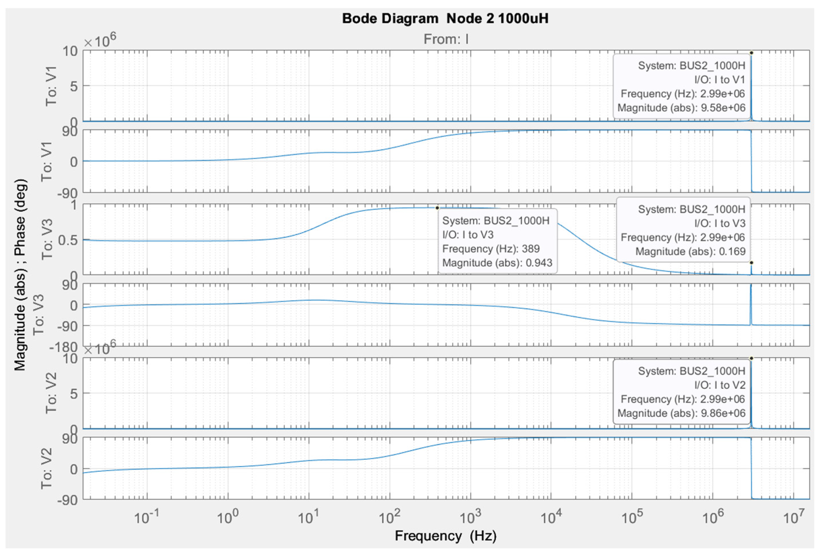
Figure 11 shows a Bode plot for a DC-DC converter with a filter inductance value of 1000 μH (Node 2). Each plot represents the response of the system under study for different points (V1, V3, V2) versus an injected input current (I) at different frequencies. Resonant frequencies and corresponding amplitudes are noted, illustrating the frequency response of the system. Typical frequencies are around 3 MHz, where the amplitude of the response is at a maximum level.
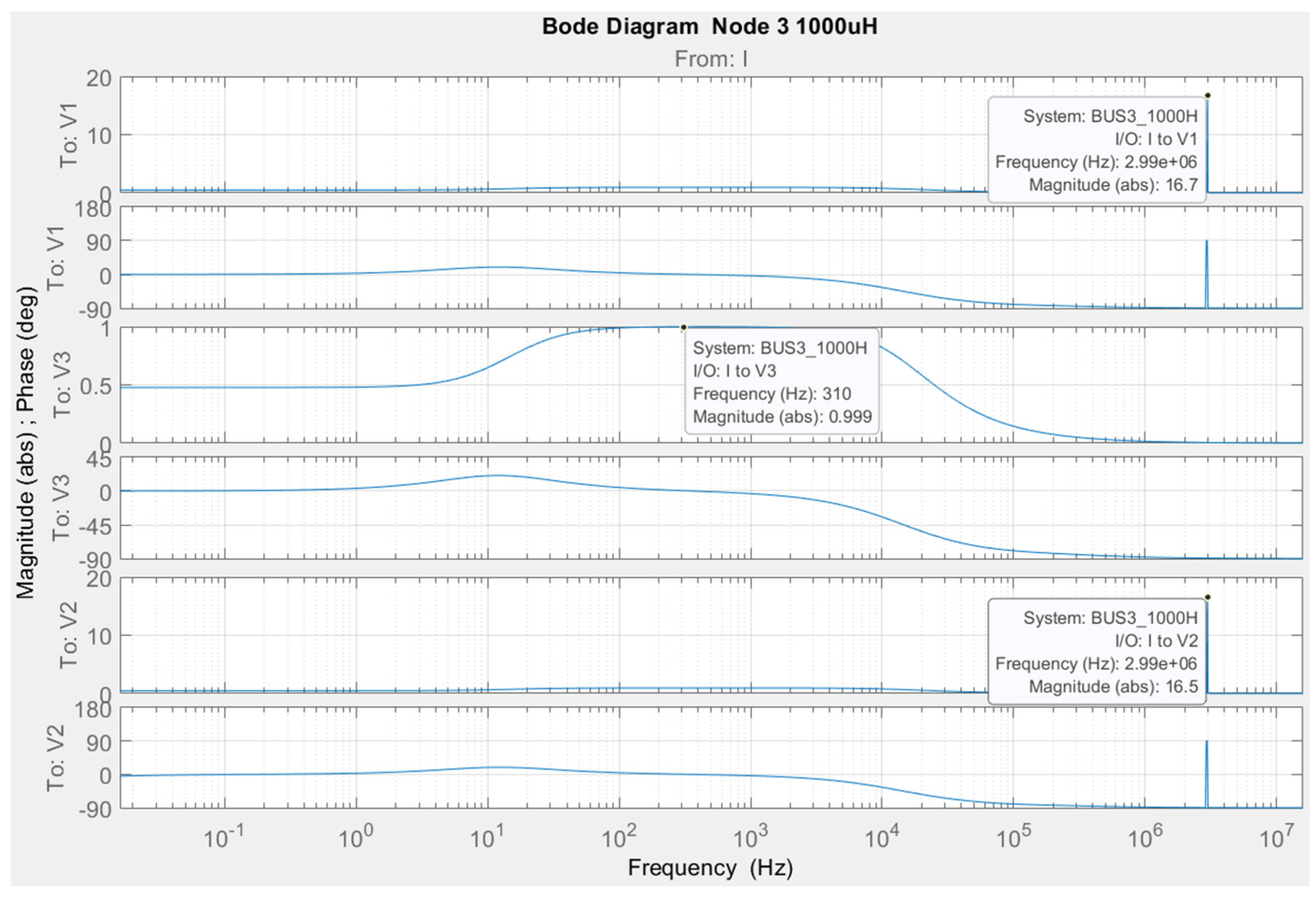
Figure 12 is a Bode plot for Node 3, at the same inductance value of 1000 μH. The plot shows the frequency response of the system in amplitude and frequency versus input current (I) at different points (V1, V3, V2). Key resonant frequencies are noted, the most notable being around 3 MHz, where significant amplitude values are observed, especially for V1 (16.7) and V2 (16.5), suggesting signal amplification in this frequency range.
Figure 13 is a Bode plot for Node 3 with an inductance of 1000 μH. The plots illustrate the frequency response of the system versus the input current (I) at various points (V1, V3, V2). Characteristic frequencies are noted, with significant amplitude values observed for V1 (16.7) and V2 (16.5) around 3 MHz. The phase response shows changes with frequency, which is important for analyzing the dynamic behavior of the system.
Figure 14, Figure 15 and Figure 16 present the simulation studies of the Buck DC-DC converter with filter inductance value L = 1500 µH.
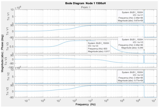
Figure 14.
Bode diagram for studying a Buck DC-DC converter, regarding Node 1 when L = 1.5 mH.
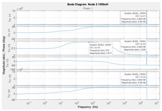
Figure 15.
Bode diagram for studying a Buck DC-DC converter, regarding Node 2 when L = 1.5 mH.
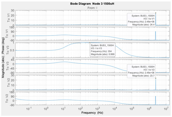
Figure 16.
Bode diagram for studying a Buck DC-DC converter, regarding Node 3 when L = 1.5 mH.
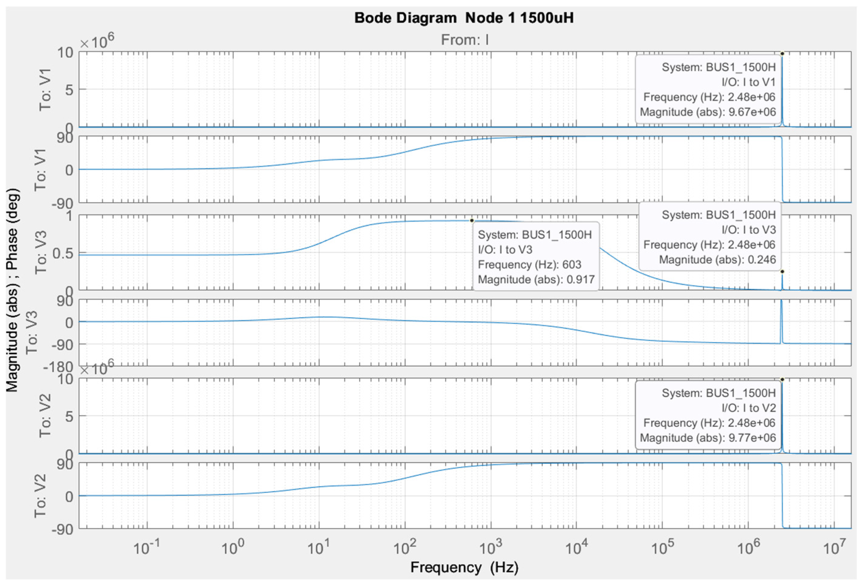
Figure 14 presents a Bode plot for Node 1 with a filter inductance value of 1500 μH. The plots show the amplitude and phase response versus frequency for different points (V1, V3, V2) at an input current (I). Key frequencies are noted, such as around 2.48 MHz, where the amplitudes of V1 and V2 reach high values (~9.67 × 10⁶ and ~9.77 × 10⁶), which may indicate resonance phenomena. At lower frequencies, for example, at 603 Hz for V3, the amplitude is significantly smaller (0.917), indicating different dynamics in this range.
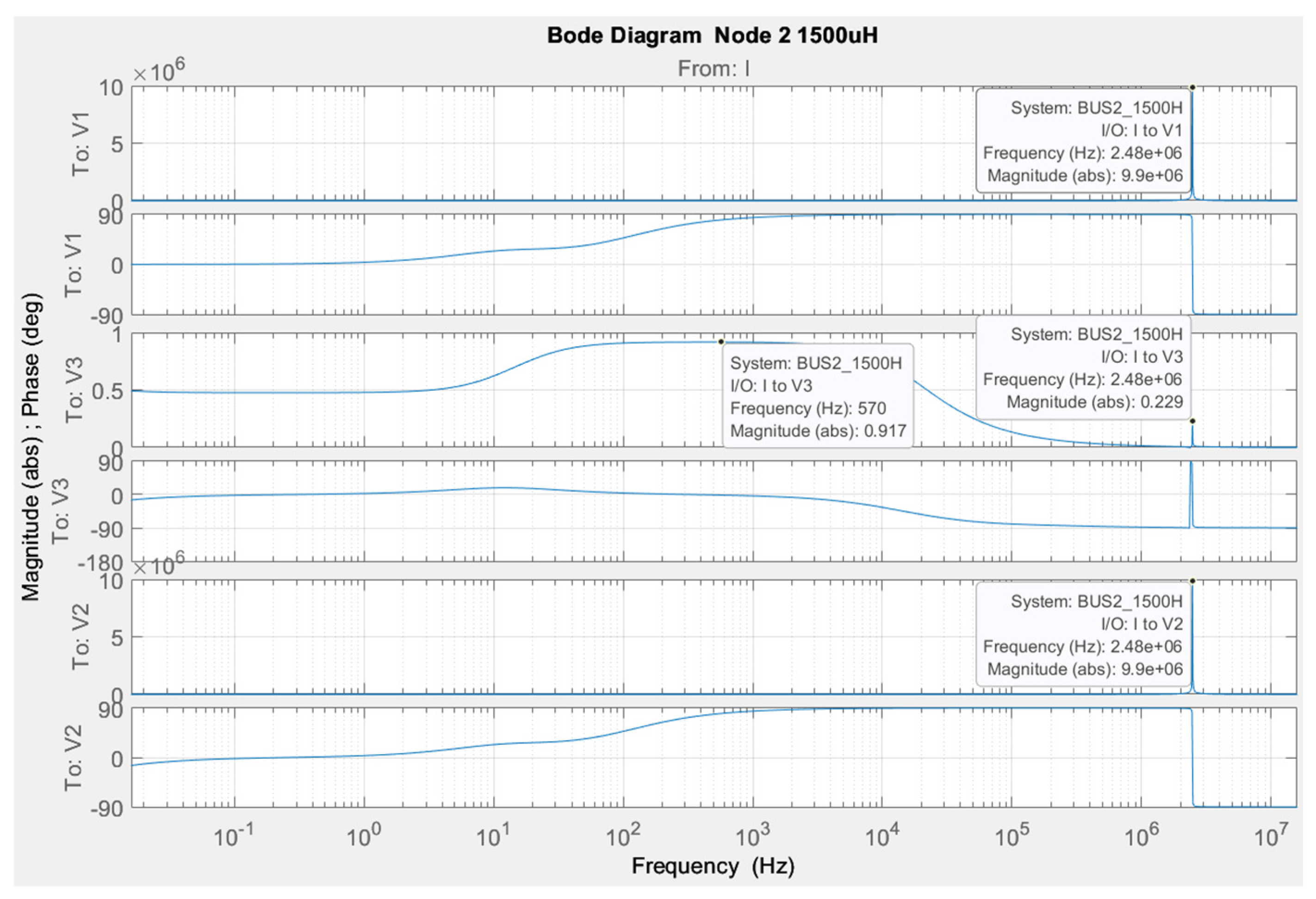
Figure 15 presents a Bode plot for Node 2 with a filter inductance of 1500 μH. It shows the amplitude and phase response as a function of frequency for different points (V1, V3, V2) at an input current (I). A significant gain is observed around 2.48 MHz, where the amplitude for V1 and V2 reaches approximately 9.9 × 10⁶, which probably indicates a resonant peak. At lower frequencies, for example, 570 Hz for V3, the amplitude is 0.917 and the phase undergoes changes, reflecting the dynamics of the system in this range.
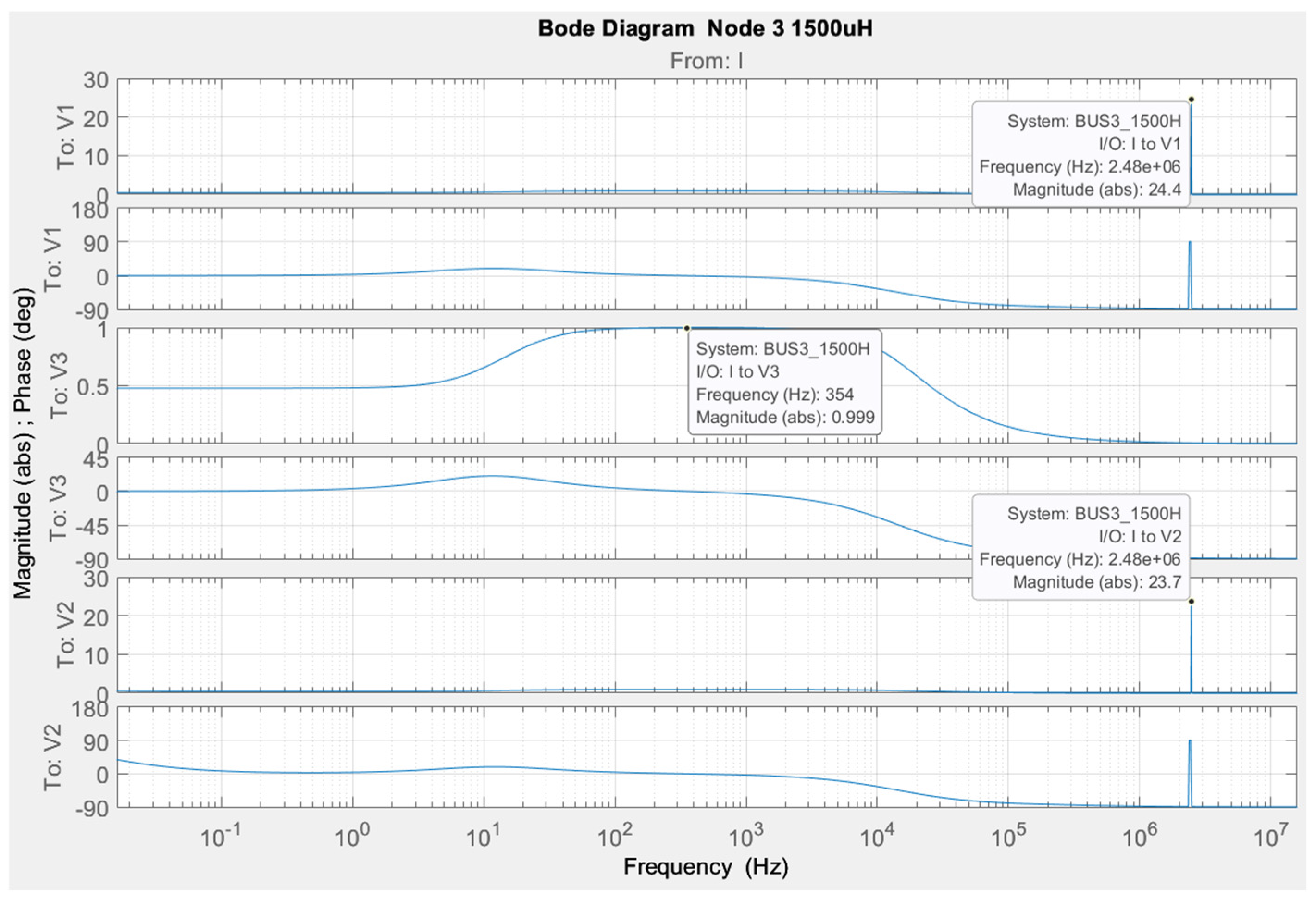
Figure 16 presents a Bode plot for Node 3 with the same inductance value of 1500 μH. The plots show the amplitude and phase response versus frequency for different points (V1, V3, V2) at an input current (I). A significant resonant peak is observed around 2.48 MHz, where the amplitudes for V1 and V2 reach 24.4 and 23.7, respectively, suggesting strong amplification in this frequency range. At lower frequencies, such as 354 Hz for V3, the amplitude is 0.999 and the phase response shows a smooth transition, which is important for understanding the dynamics of the system.
From the presented simulation results for the Buck DC-DC converter, characteristic peaks expressing the frequency response of the respective nodes are visible. A dependence is observed at Node three, where, regardless of the implemented perturbation, the amplitude curve does not change. Also, a characteristic plateau is observed with a wide frequency range from 10 Hz to 1 × 10⁵ Hz.
The response of the three nodes is isolated at one characteristic frequency, changing only the magnitude, but not the frequency range. For example, it can be seen that, as the inductance value increases, the response of Node 1 also increases when a disturbance is injected into Node 3. Also, at Node 1, a characteristic frequency plateau is observed in a range similar to Node 3, but with a smaller amplitude. The only noticeable increase in frequency response is around 1 × 10⁷ Hz.
When implementing a disturbance in Node 3, the response of Node 2 overlaps with Node 1. This is due to the principle of operation of the circuit, due to the series-connected inductance to the load.
Similar studies for the Boost DC-DC converter with the same values of load resistance R = 12 Ω, output capacitance with value C = 5 µF, and change in filter inductance with initial value of L = 100 µH and increase by 5, 10, and 15 times.
The simulation circuit of the Boost DC-DC converter is presented in Figure 17. A similar modeling approach was used, and a substitute circuit of the converter was used.
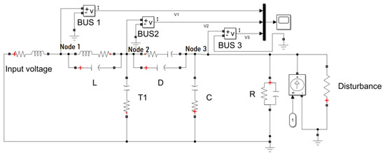
Figure 17.
Simulation scheme in Boost DC-DC converter in MATLAB/Simulink.
Figure 18, Figure 19 and Figure 20 show the simulation results when injecting a relative disturbance unit. Magnitude and the phase in each node are presented sequentially from top to bottom. These results were conducted with an inductance value of L = 100 µH.
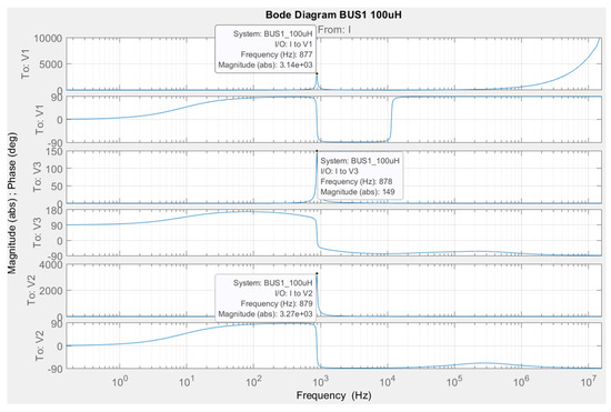
Figure 18.
Bode diagram for studying a Boost DC-DC converter, regarding Bus 1 when L = 100 µH.
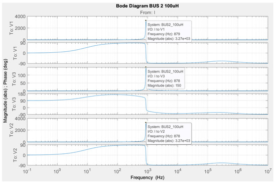
Figure 19.
Bode diagram for studying a Boost DC-DC converter, regarding Bus 2 when L = 100 µH.
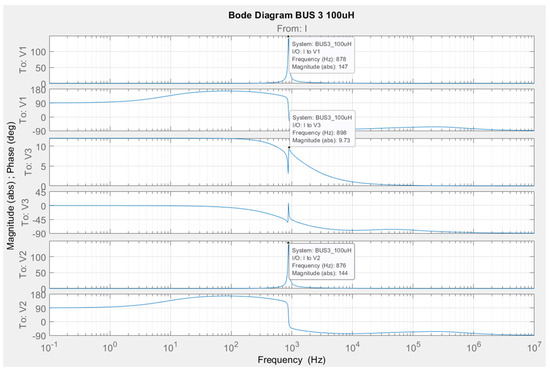
Figure 20.
Bode diagram for studying a Boost DC-DC converter, regarding Bus 3 when L = 100 µH.
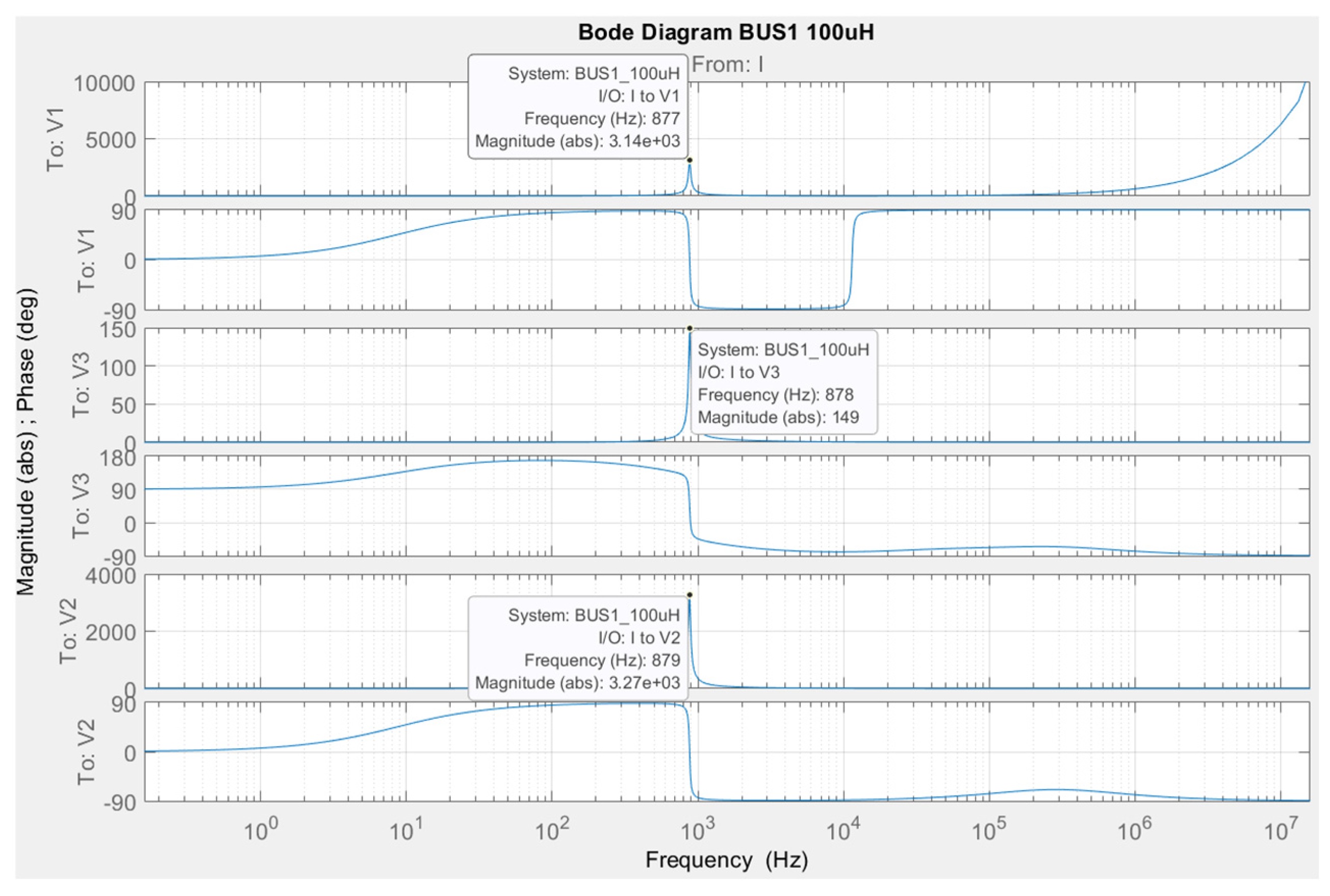
Figure 18 is a Bode plot for a Boost DC-DC converter, with BUS1 having a filter inductance value of 100 μH. The plots show the amplitude and phase response versus frequency for different points (V1, V3, V2) at an input current (I). A distinct resonance peak is observed around 877–879 Hz, where the amplitudes for V1 and V2 reach high values (3146 and 3270 respectively), while for V3 the amplitude is significantly lower (149). This resonance frequency shows the frequency response of the system and its behavior at different input frequencies.
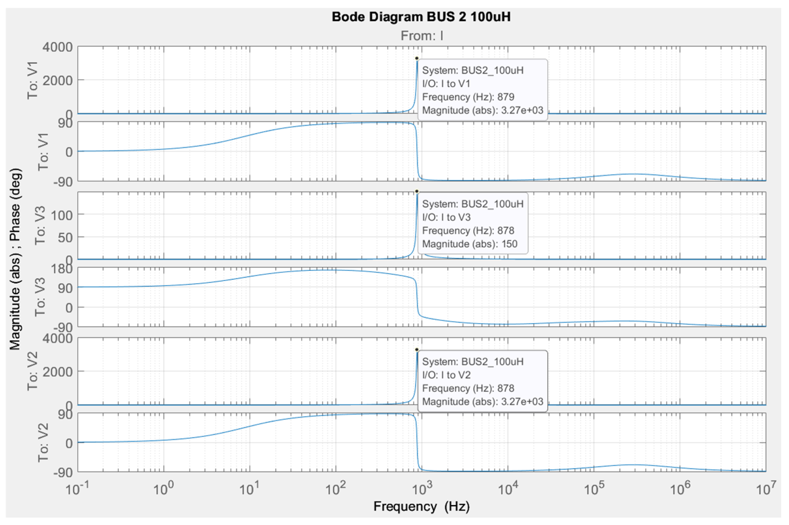
Figure 19 presents a Bode plot for the same DC-DC converter, regarding BUS2 at a filter inductance of 100 μH. The plots show the amplitude and phase response versus frequency for different points (V1, V3, V2) at an input current (I). A clear resonance peak is observed around 878–879 Hz, where the amplitudes for V1 and V2 reach 3270, while for V3 the value is significantly lower (150). This indicates that the system exhibits a strong frequency response in this range, which is important for understanding its dynamics and potential resonance effects.
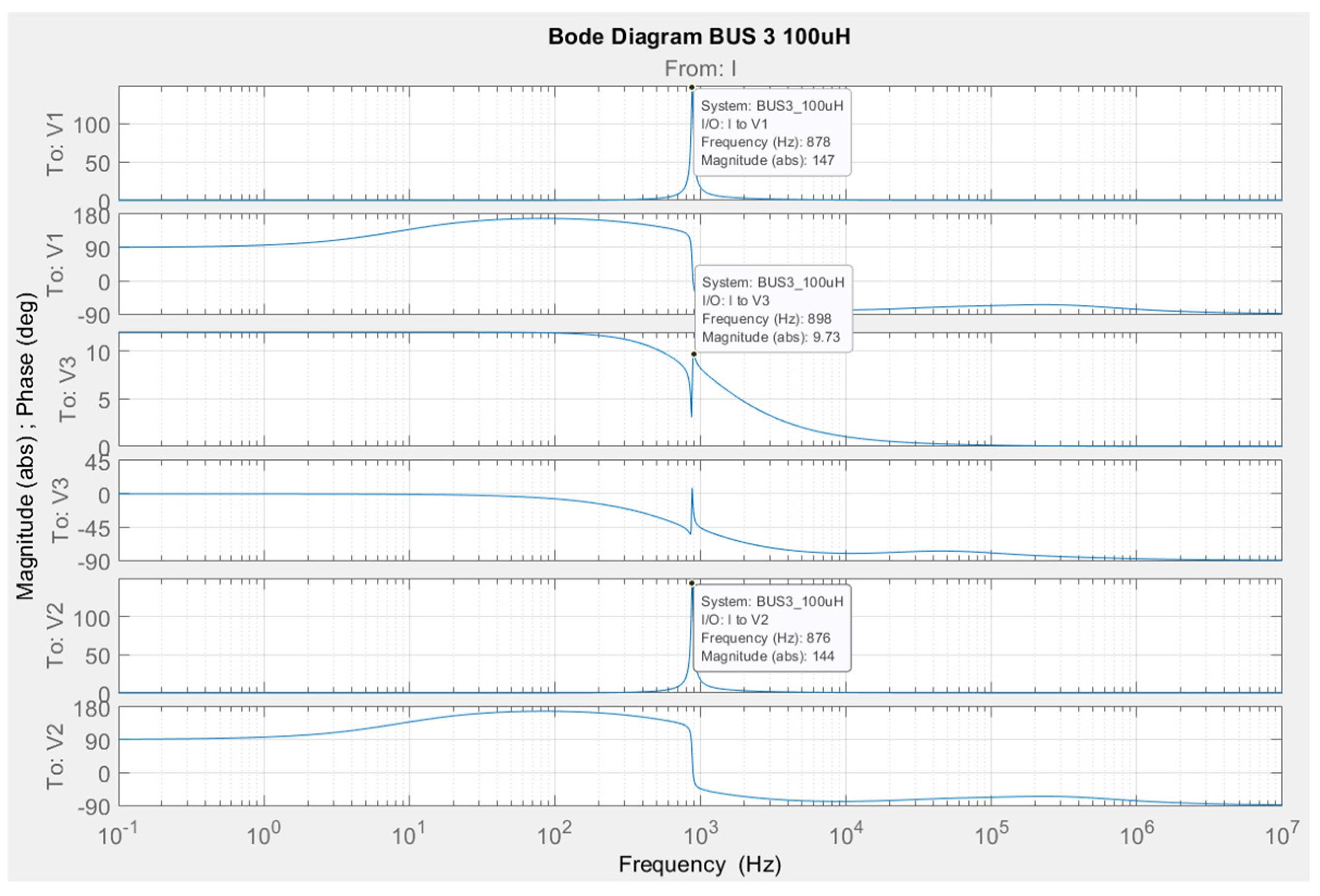
Figure 20 is a Bode plot for BUS3 with an inductance of 100 μH. The plots illustrate the amplitude and phase response versus frequency for different points (V1, V3, V2) at an input current (I). Resonance peaks are observed around 876–878 Hz, where the amplitudes for V1 and V2 reach 147 and 144, respectively, while for V3 the value is significantly lower (9.73 at 898 Hz). This indicates that the system exhibits a specific frequency response, with different nodes having different sensitivities in this range.
Figure 21, Figure 22 and Figure 23 show simulation results for the value of the inductance L = 500 µH.
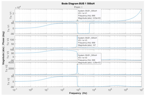
Figure 21.
Bode diagram for studying a Boost DC-DC converter, regarding Bus 1 when L = 500 µH.
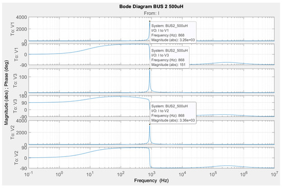
Figure 22.
Bode diagram for studying a Boost DC-DC converter, regarding Bus 2 when L = 500 µH.
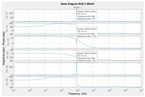
Figure 23.
Bode diagram for studying a Boost DC-DC converter, regarding Bus 3 when L = 500 µH.
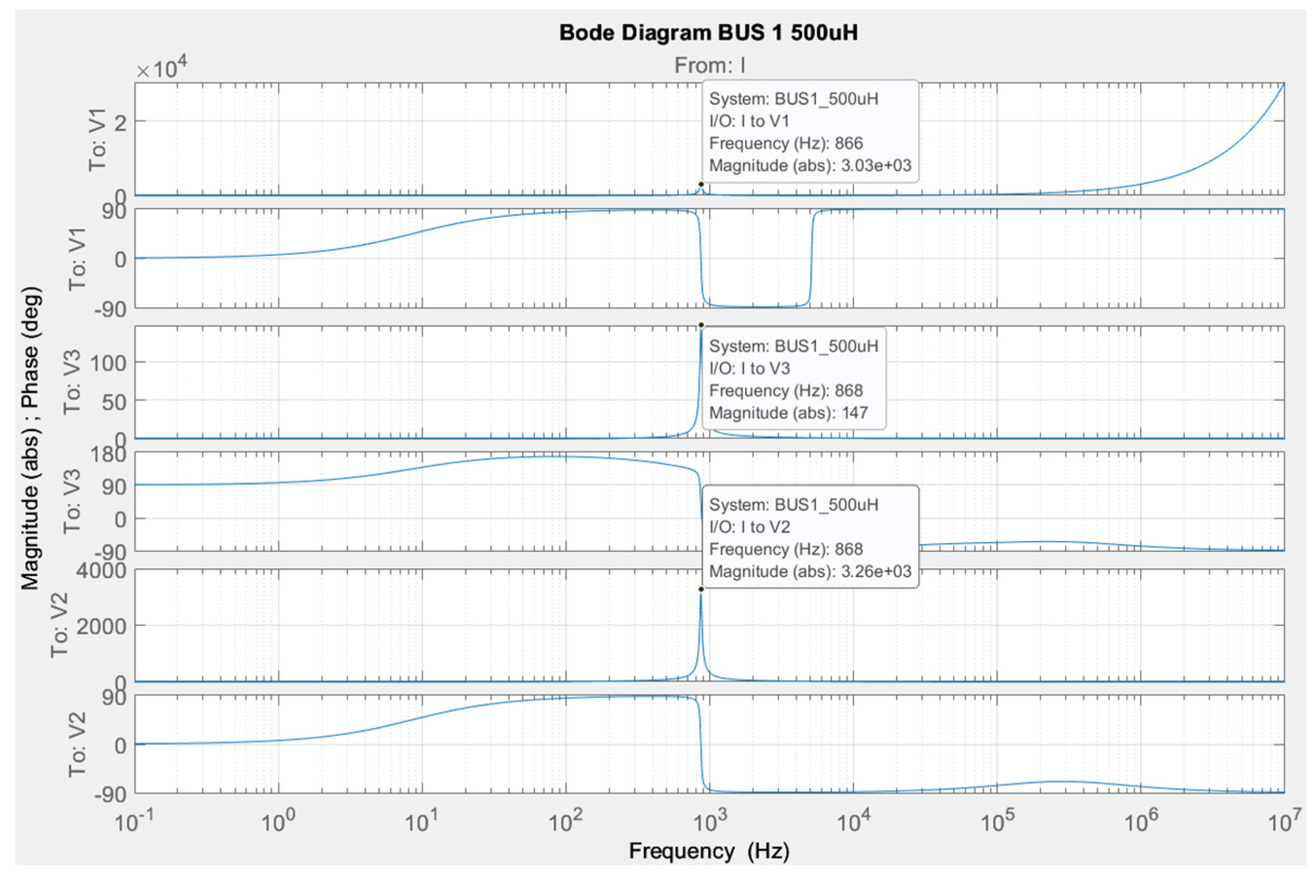
Figure 21 is a Bode plot for a Boost DC-DC converter, with respect to BUS1 at a filter inductance value of 500 μH. The plots show the amplitude and phase response versus frequency for different points (V1, V3, V2) at an input current (I). Distinct resonance peaks are observed around 866–868 Hz, where the amplitudes for V1 and V2 reach 3.03 × 10³ and 3.26 × 10³, respectively, while for V3 the value is significantly lower (147). This indicates that the system has a strong frequency response in this range, which may be essential for its behavior under different input signals.
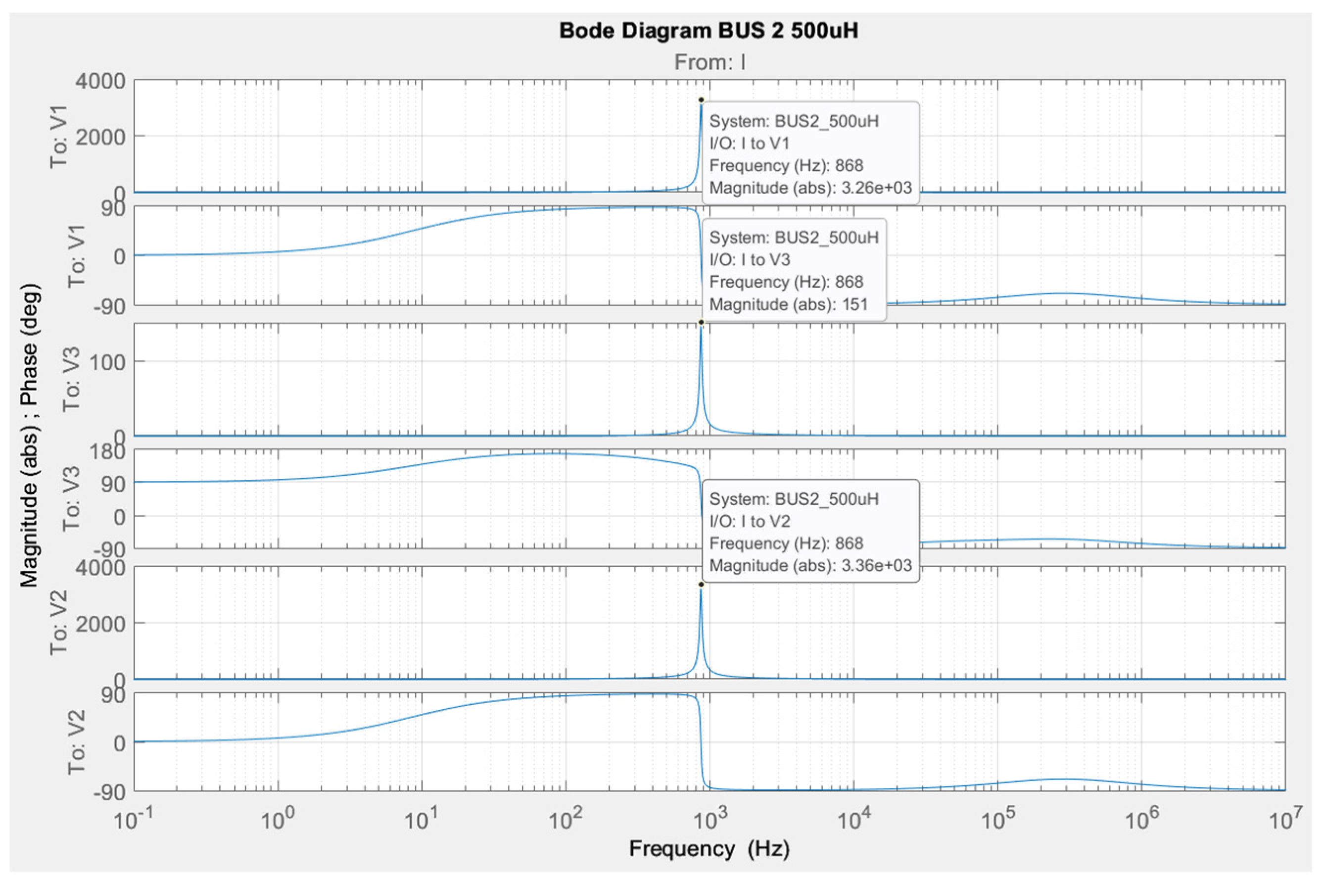
Figure 22 presents a Bode plot for the same DC-DC converter with respect to BUS2 at a filter inductance value of 500 μH. The plots show the amplitude and phase response versus frequency for different points (V1, V3, V2) at an input current (I). Resonance peaks are observed around 868 Hz, where the amplitudes for V1 and V2 reach 3.26 × 10³ and 3.36 × 10³, respectively, while for V3 the value is significantly lower (151). This indicates that the system has a distinct frequency response in this range, with V1 and V2 demonstrating the strongest gain.
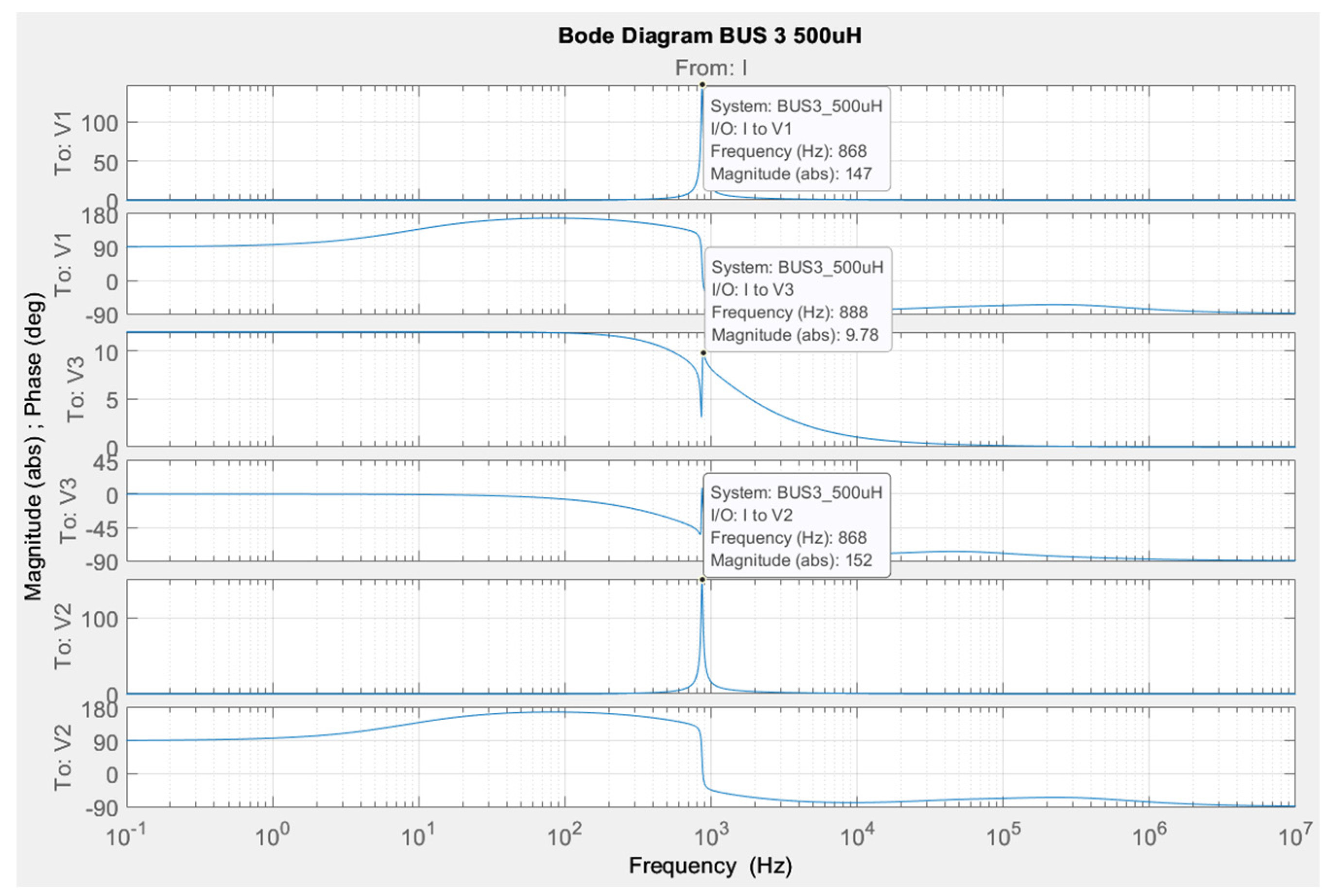
Figure 23 is a Bode plot for BUS3 with an inductance value of 500 μH. The plots illustrate the amplitude and phase response versus frequency for different points (V1, V3, V2) at an input current (I). Resonance peaks are observed around 868 Hz for V1 and V2, with amplitudes of 147 and 152, respectively, while for V3 the peak is at 888 Hz with an amplitude of 9.78. This shows that the system exhibits different frequency sensitivity depending on the measurement point, with V1 and V2 demonstrating the strongest response in the main resonance range.
Figure 24, Figure 25 and Figure 26 show a simulation results for the value of the inductance L = 1000 µH.
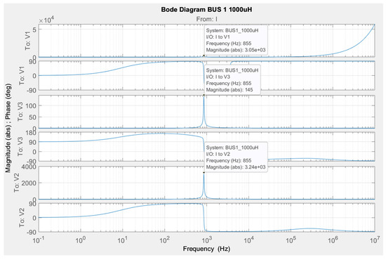
Figure 24.
Bode diagram for studying a Boost DC-DC converter, regarding Bus 1 when L = 1 mH.
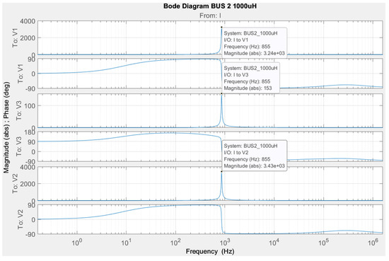
Figure 25.
Bode diagram for studying a Boost DC-DC converter, regarding Bus 2 when L = 1 mH.
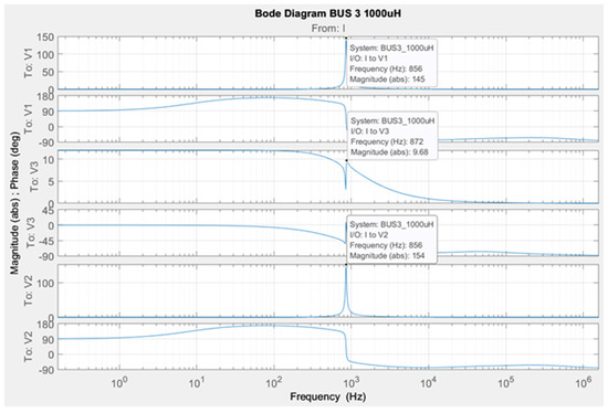
Figure 26.
Bode diagram for studying a Boost DC-DC converter, regarding Bus 3 when L = 1 mH.
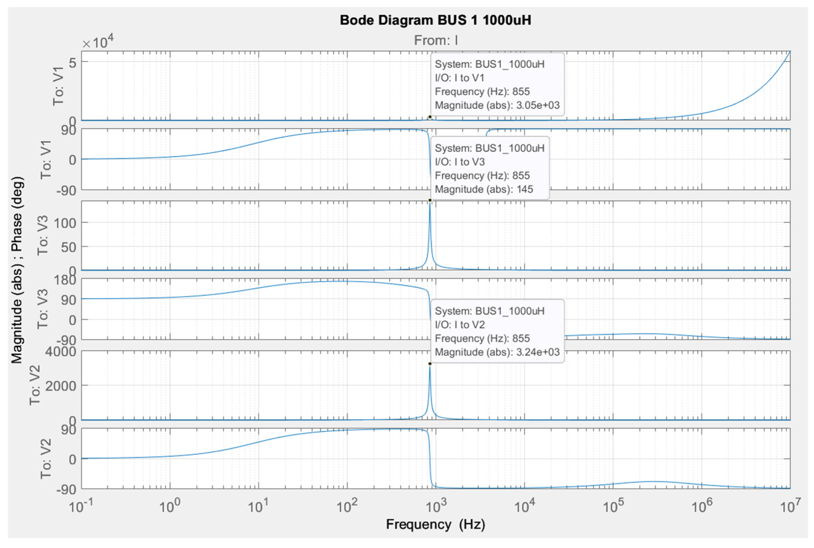
Figure 24 is a Bode plot for Boost DC-DC on BUS1 with a filter inductance value of 1000 μH. The plots show the amplitude and phase response versus frequency for different points (V1, V3, V2) at input current (I). A distinct resonance peak is observed around 855 Hz, where the amplitudes for V1 and V2 reach 3.05 × 10³ and 3.24 × 10³, respectively, while for V3 the value is significantly lower (145). This indicates that the system has a strong frequency response in this range, which is important for analyzing its resonance characteristics and its behavior at different input frequencies.
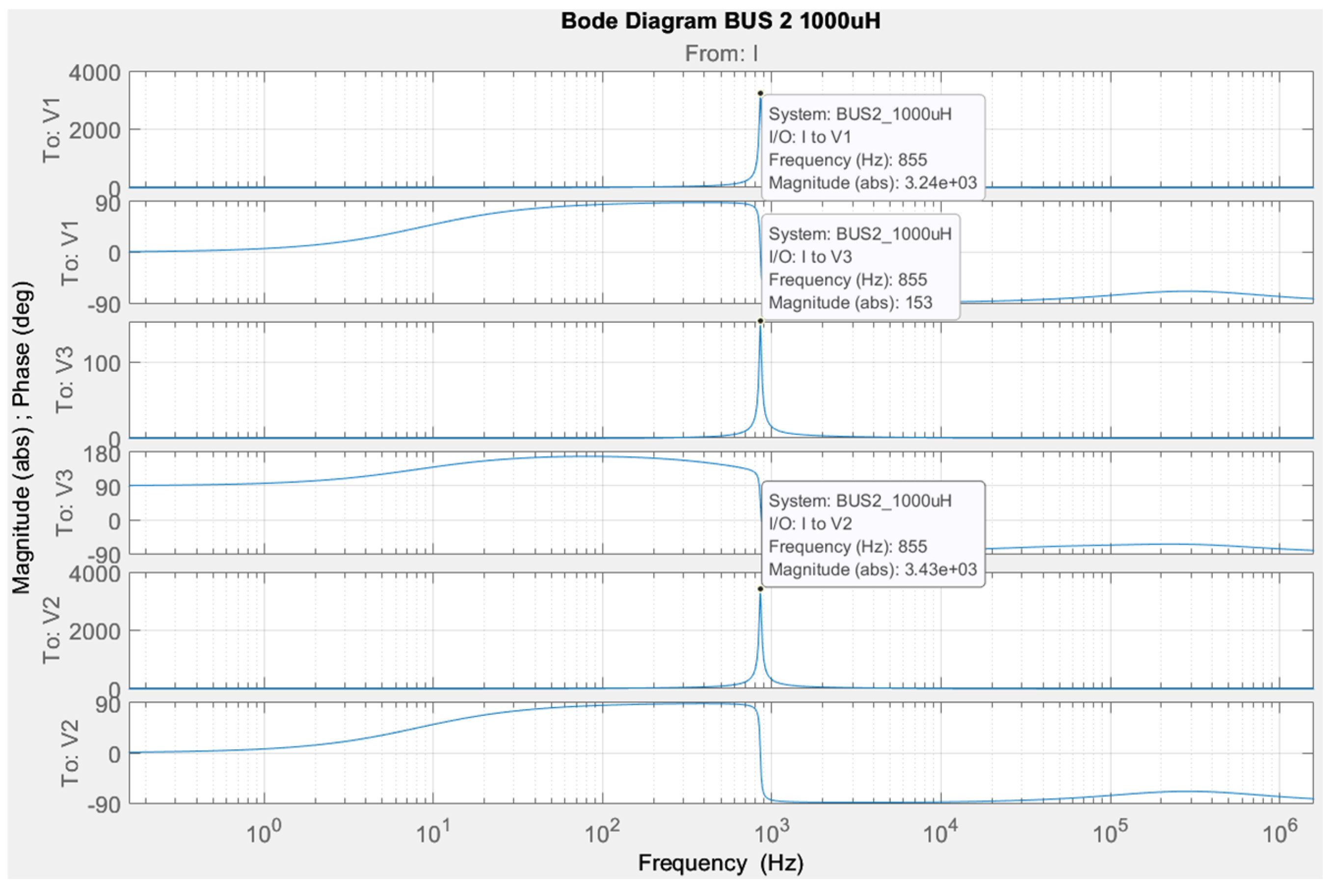
Figure 25 is a Bode plot for Boost DC-DC, regarding BUS2 at an inductance value of 1000 μH. The plots show the amplitude and phase response versus frequency for different points (V1, V3, V2) at an input current (I). A distinct resonant peak is observed around 855 Hz, where the amplitudes for V1 and V2 reach 3.24 × 10³ and 3.43 × 10³, respectively, while for V3 the value is significantly lower (153). This indicates that the system has a clear resonant response in this frequency range, with V1 and V2 demonstrating the highest gain.
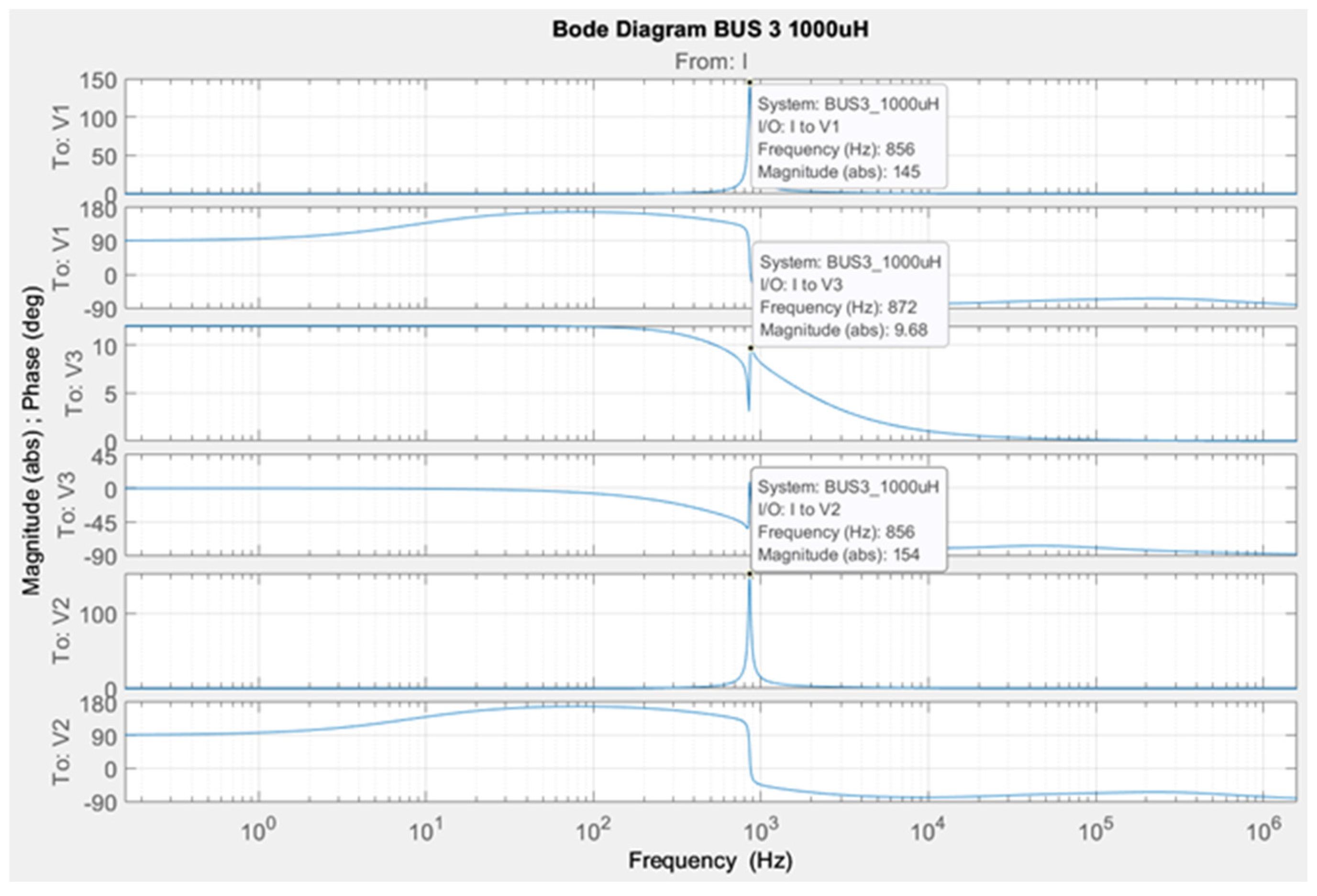
Figure 26 is a Bode plot for BUS3 for a filter inductance of 1000 μH. The plots show the amplitude and phase response versus frequency for different points (V1, V3, V2) at an input current (I). Resonance peaks are observed around 856 Hz for V1 and V2 with amplitudes of 145 and 154 respectively, while for V3 the peak is at 872 Hz with amplitude 9.68. This shows that the system exhibits different frequency sensitivity depending on the measurement point, with V1 and V2 demonstrating the strongest response in the main resonance range.
Figure 27, Figure 28 and Figure 29 show simulation results for the value of the inductance L = 1500 µH.
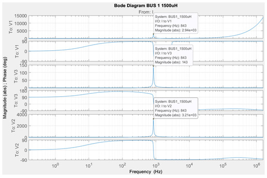
Figure 27.
Bode diagram for studying a Boost DC-DC converter, regarding Bus 1 when L = 1500 µH.
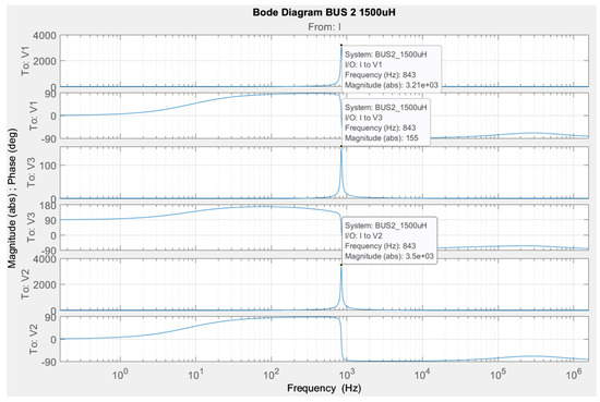
Figure 28.
Bode diagram for studying a Boost DC-DC converter, regarding Bus 2 when L = 1500 µH.
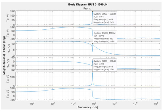
Figure 29.
Bode diagram for studying a Boost DC-DC converter, regarding Bus 3 when L = 1500 µH.
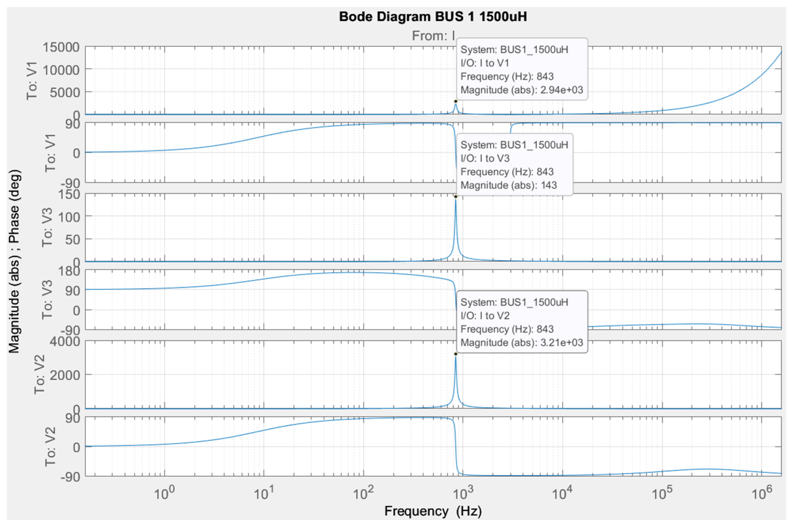
Figure 27 is a Bode plot for a Boost DC-DC converter, with respect to BUS1 at a filter inductance value of 1500 μH. The plots show the amplitude and phase response versus frequency for different points (V1, V3, V2) at an input current (I). A distinct resonant peak is observed around 843 Hz, where the amplitudes for V1 and V2 reach 2.94 × 10³ and 3.21 × 10³, respectively, while for V3 the value is significantly lower (143). This indicates that the system has a clear resonant response in this frequency range, with V1 and V2 demonstrating the highest gain.
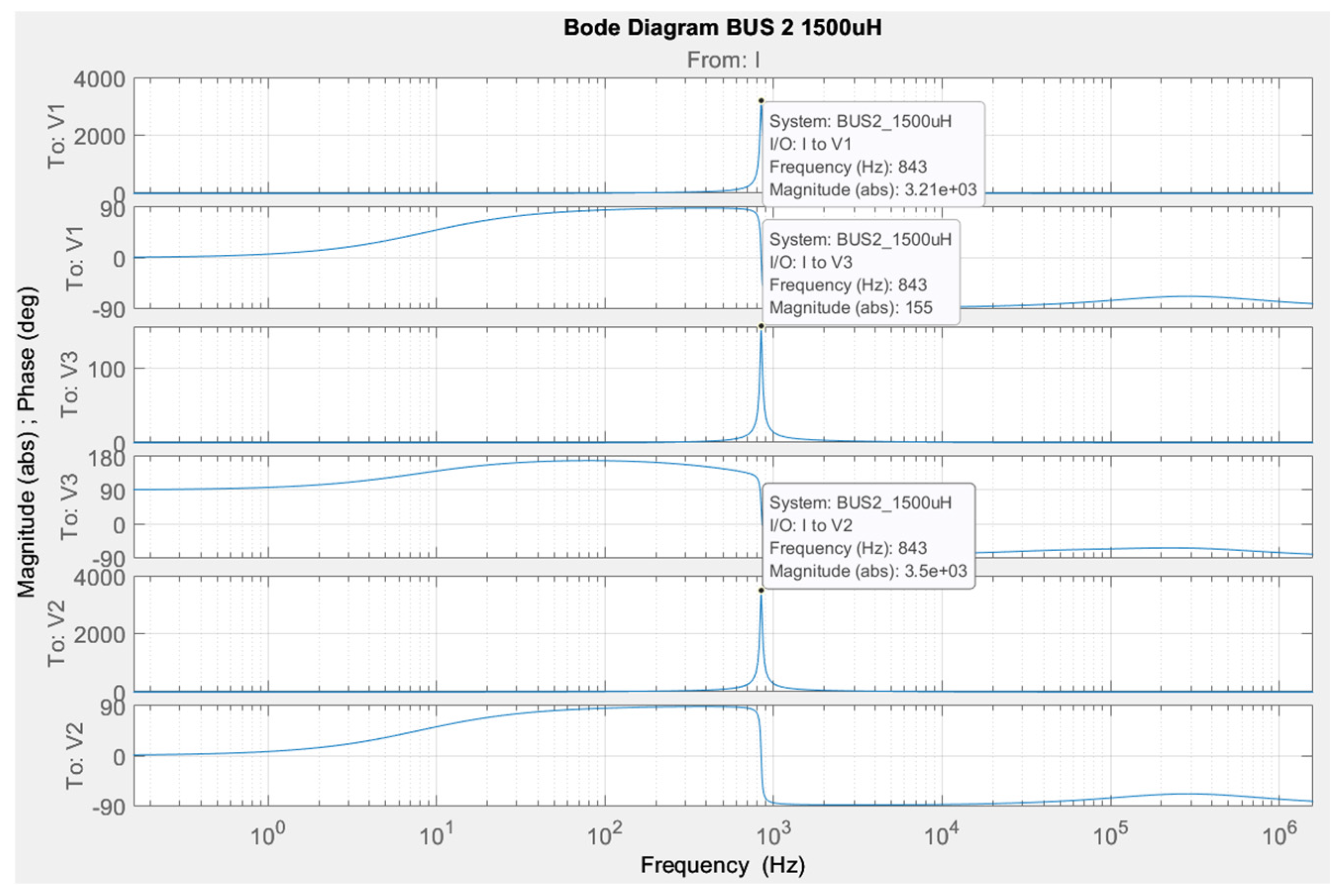
Figure 28 is a Bode plot for a Boost DC-DC converter, with respect to BUS2 at an inductance of 1500 μH. The plots show the amplitude and phase response versus frequency for different points (V1, V3, V2) at an input current (I). A distinct resonant peak is observed around 843 Hz, where the amplitudes for V1 and V2 reach 3.21 × 10³ and 3.5 × 10³, respectively, while for V3 the value is significantly lower (155). This indicates that the system exhibits a pronounced resonant response in this frequency range, with V1 and V2 demonstrating the highest gain.
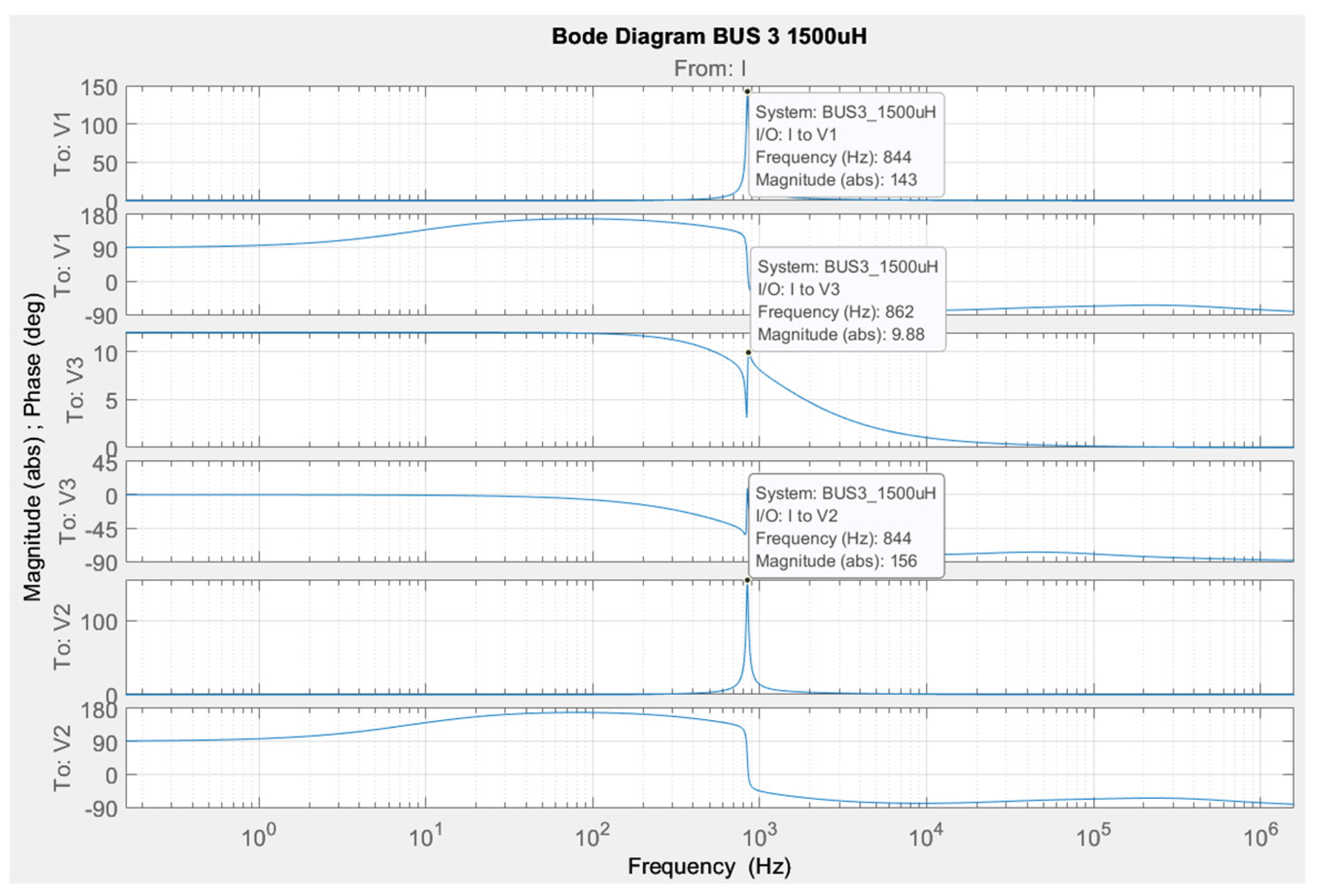
Figure 29 is a Bode plot for the same DC-DC converter, for BUS3 with a filter inductance of 1500 μH. The plots show the amplitude and phase response versus frequency for different points (V1, V3, V2) at an input current (I). A resonant peak is observed around 844 Hz for V1 and V2, with amplitudes of 143 and 156, respectively, while for V3 the peak is at 862 Hz with an amplitude of 9.88. This shows that the system has different frequency sensitivity depending on the measured point, with V1 and V2 demonstrating the strongest gain in the fundamental resonant range.
From the presented simulation results, it is observed that, when a disturbance is injected into Node 3, the response of Nodes 1 and 2 is not affected by the change in the inductance value. The impact of Node 1 also does not affect the response of the other three nodes to changes in inductance. The impact of Node 2 significantly affects the phase variation of Node 3.
Similar studies have been conducted with the Buck-Boost converter. Its replacement scheme is presented in Figure 30. The parameters used for the load and the output capacitance are the same. The model is realized in MATLAB/Simulink. The purpose of studying the Boost-Buck rebase converter is to determine the frequency range in which resonance could occur in the circuit, when a disturbance is injected into each of the nodes of the circuit. Simulation studies are presented in four cases when the value of the inductance is changed. The initial value is L = 100 µH, and then it is increased by 5, 10, and 15 times.
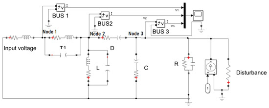
Figure 30.
Simulation scheme of Buck-Boost DC-DC converter in MATLAB/Simulink.
Figure 31, Figure 32 and Figure 33 show simulation results for the value of the inductance L = 100 µH.
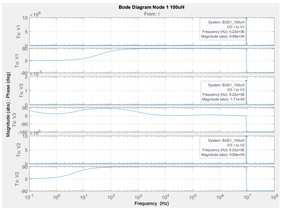
Figure 31.
Bode diagram for studying a Buck-Boost DC-DC converter, regarding Node 1 when L = 100 µH.
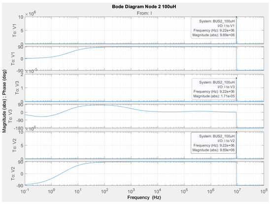
Figure 32.
Bode diagram for studying a Buck-Boost DC-DC converter, regarding Node 2 when L = 100 µH.
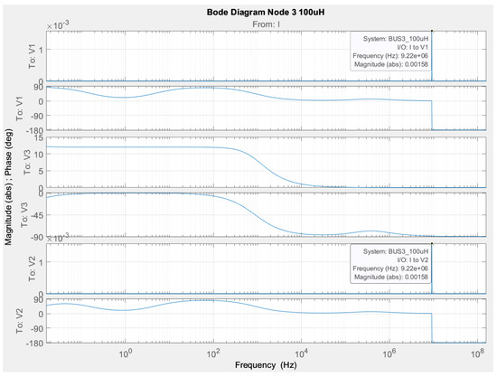
Figure 33.
Bode diagram for studying a Buck-Boost DC-DC converter, regarding Node 1 when L = 100 µH.
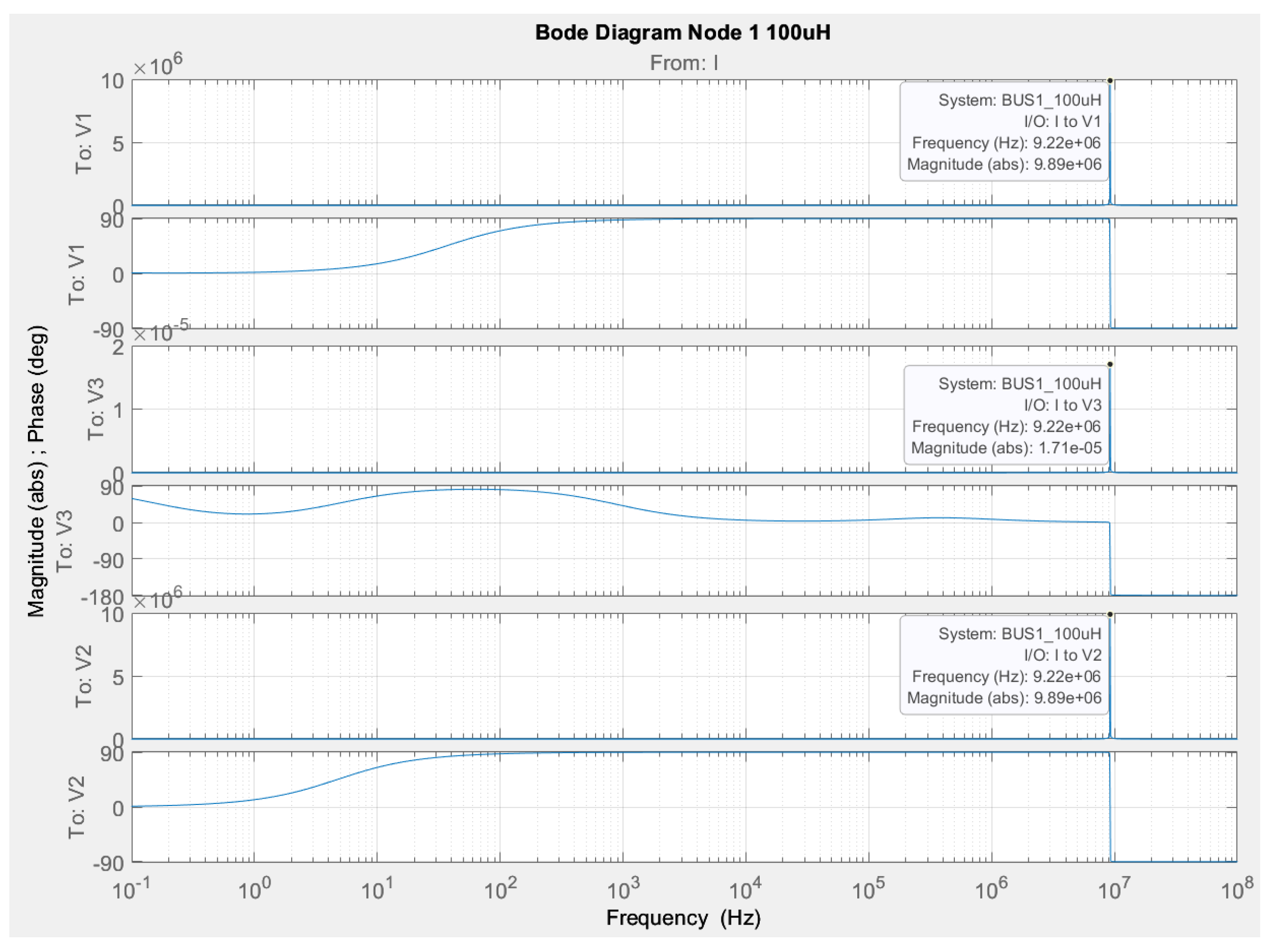
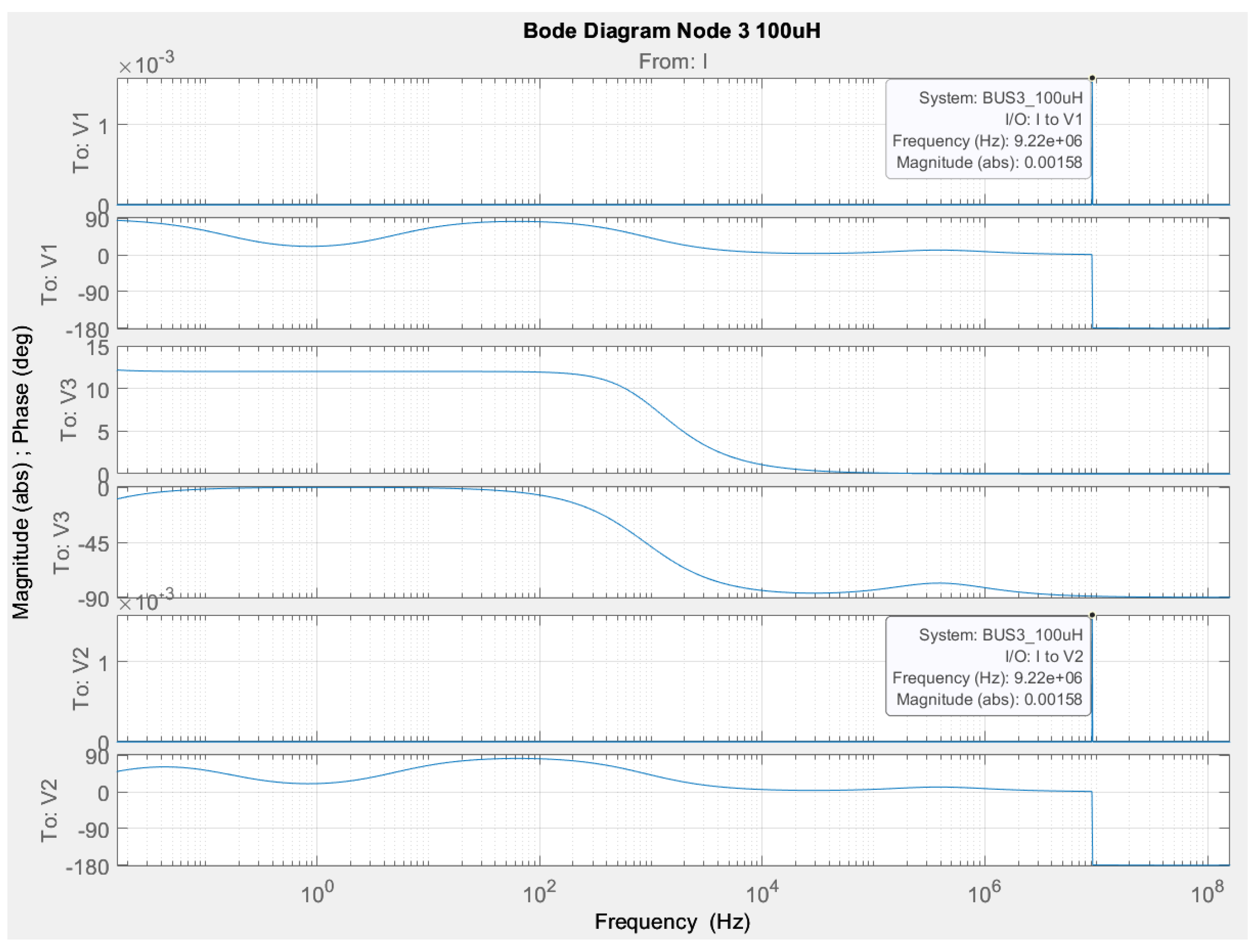
Figure 31 is a Bode plot of a Buck-Boost DC-DC converter, about Node 1 with a filter inductance value of 100 μH. The plots show the amplitude and phase response versus frequency for different points (V1, V3, V2) at an input current (I). A resonant peak is observed around 9.22 MHz, where the amplitudes for V1 and V2 reach high values (8.98 × 10⁶), while for V3 the value is significantly lower (1.71 × 10⁻⁵). This shows that the system exhibits a strong frequency response in this range, with V1 and V2 demonstrating the highest gain, which is important for the analysis of its dynamic characteristics and applications.
Figure 32 is a Bode plot of a Buck-Boost DC-DC converter, about Node 2 with a filter inductance of 100 μH. The plots show the amplitude and phase response versus frequency for different points (V1, V3, V2) at an input current (I). A resonant peak is observed around 9.22 MHz, where the amplitudes for V1 and V2 reach high values (8.98 × 10⁶), while for V3 the value is significantly lower (1.71 × 10⁻⁵). This shows that the system exhibits a strong frequency response in this range, with V1 and V2 demonstrating the highest gain.
Figure 33 is a Bode plot for the same converter, regarding Node 3 at a filter inductance of 100 μH. The plots show the amplitude and phase response versus frequency for different points (V1, V3, V2) at an input current (I). A frequency response is observed around 9.22 MHz, but the amplitudes for V1 and V2 are significantly lower (0.00158), suggesting that this node does not exhibit the same resonant effect as in the previous cases. The phase response shows a smooth transition depending on the frequency.
Figure 34, Figure 35 and Figure 36 show simulation results for the value of the inductance L = 500 µH.
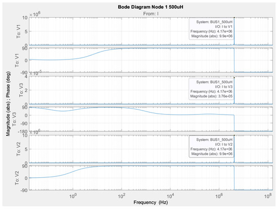
Figure 34.
Bode diagram for studying a Buck-Boost DC-DC converter, regarding Node 1 when L = 500 µH.
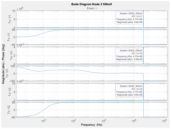
Figure 35.
Bode diagram for studying a Buck-Boost DC-DC converter, regarding Node 2 when L = 500 µH.
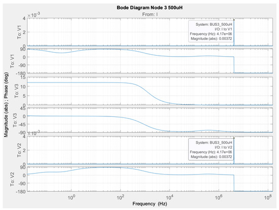
Figure 36.
Bode diagram for studying a Buck-Boost DC-DC converter, regarding Node 3 when L = 500 µH.
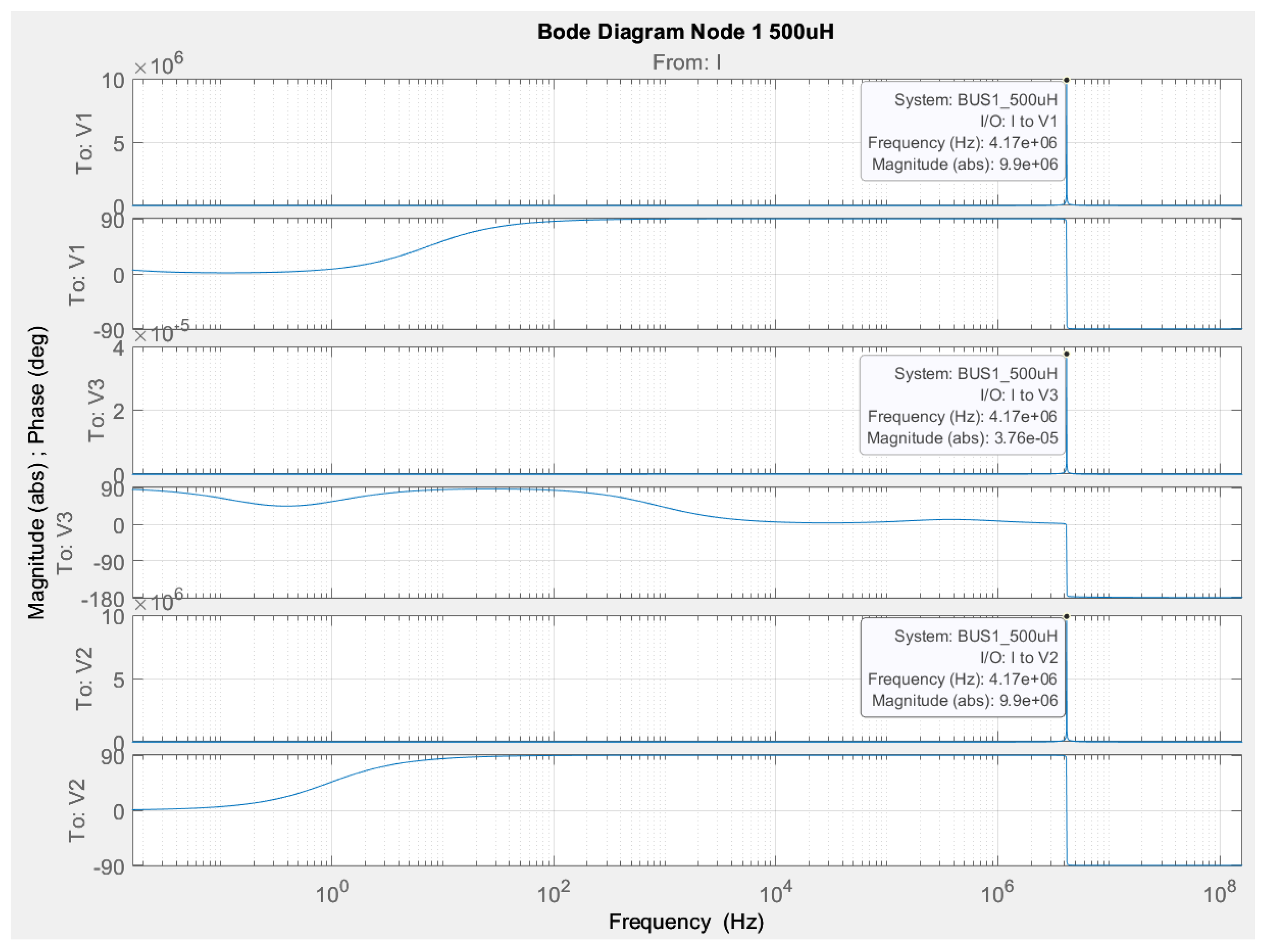
Figure 34 is a Bode plot for Node 1 with an inductance of 500 μH. The plots show the amplitude and phase response versus frequency for different points (V1, V3, V2) at an input current (I). A resonant peak is observed around 4.17 MHz, where the amplitudes for V1 and V2 reach high values (9.9 × 10⁶), while for V3 the value is significantly lower (3.76 × 10⁻⁵). This indicates that the system exhibits a strong frequency response in this range, with V1 and V2 demonstrating the highest gain.
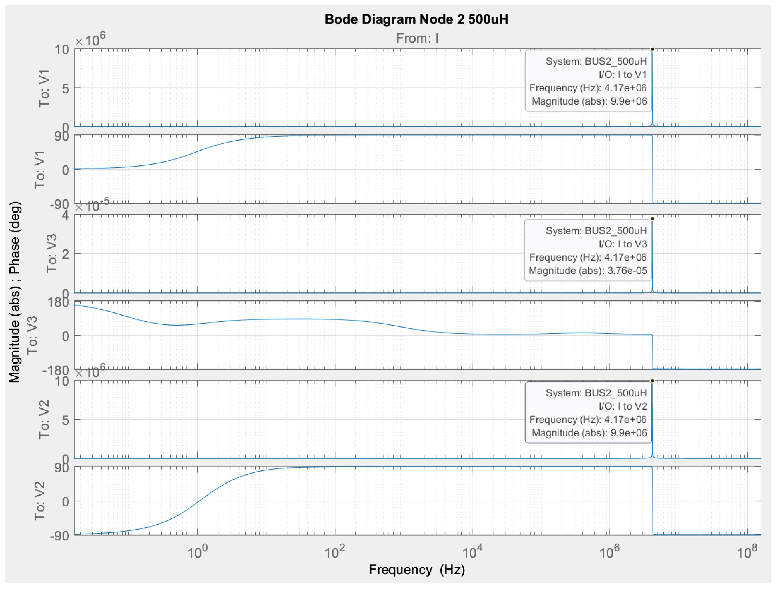
Figure 35 is a Bode plot for Node 2 with an inductance of 500 μH. The plots show the amplitude and phase response versus frequency for different points (V1, V3, V2) at an input current (I). A resonant peak is observed around 4.17 MHz, where the amplitudes for V1 and V2 reach high values (9.9 × 10⁶), while for V3 the value is significantly lower (3.76 × 10⁻⁵). This indicates that the system exhibits a strong frequency response in this range, with V1 and V2 demonstrating the highest gain.
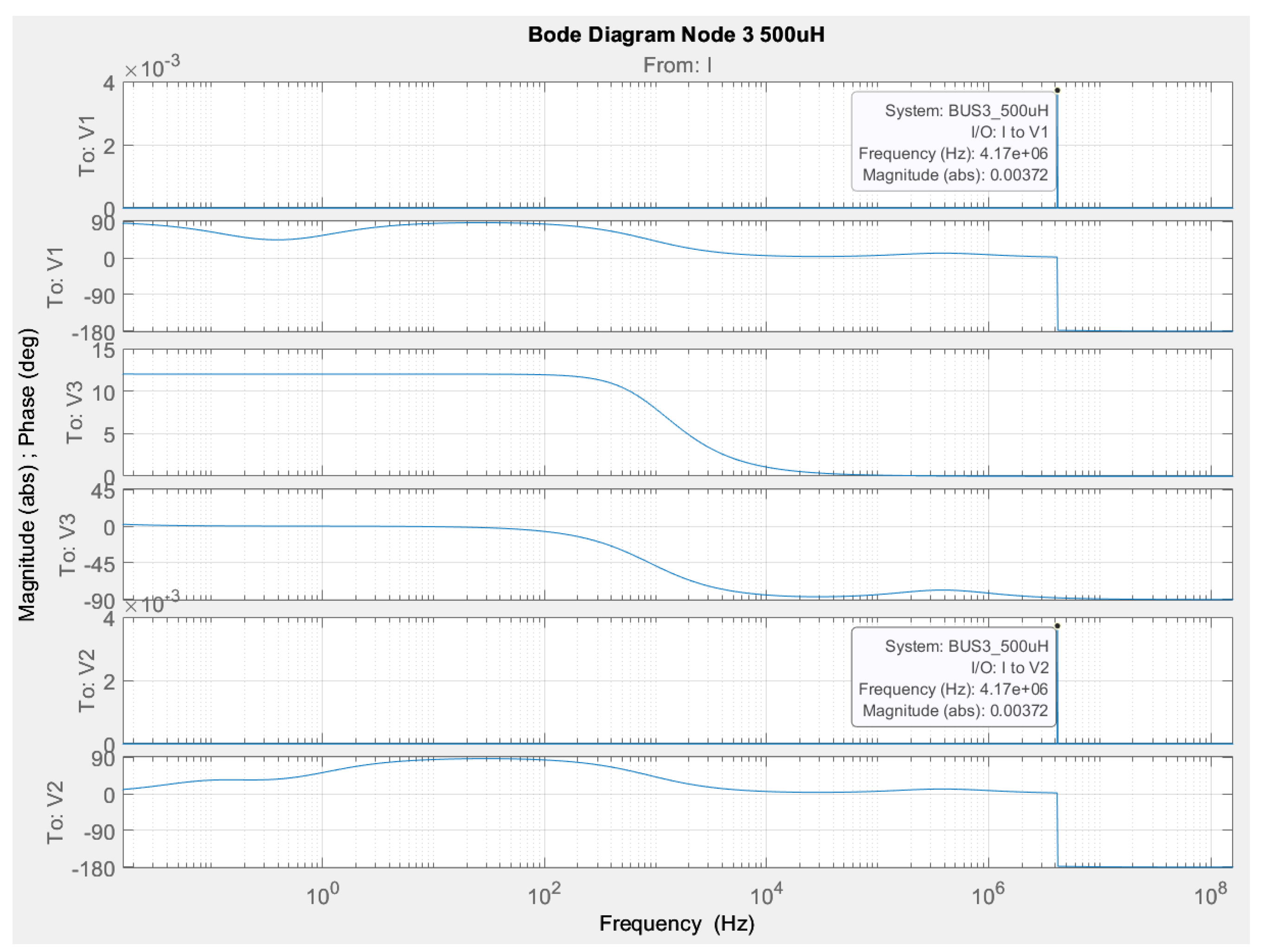
Figure 36 is a Bode plot for Node 3 with an inductance of 500 μH. The plots show the amplitude and phase response versus frequency for different points (V1, V3, V2) at an input current (I). A frequency response is observed around 4.17 MHz, but the amplitudes for V1 and V2 are significantly lower (0.00372), suggesting that this node does not exhibit the same resonant effect as in the previous cases. The phase response shows a smooth transition depending on frequency.
Figure 37, Figure 38 and Figure 39 show simulation results for the value of the inductance L = 1000 µH.
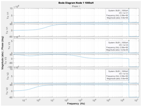
Figure 37.
Bode diagram for studying a Buck-Boost DC-DC converter, regarding Node 1 when L = 1000 µH.
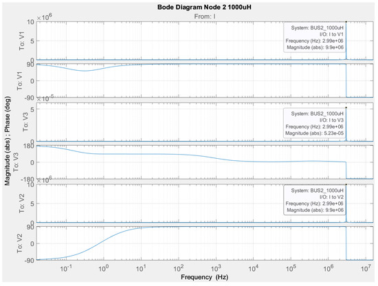
Figure 38.
Bode diagram for studying a Buck-Boost DC-DC converter, regarding Node 2 when L = 1000 µH.
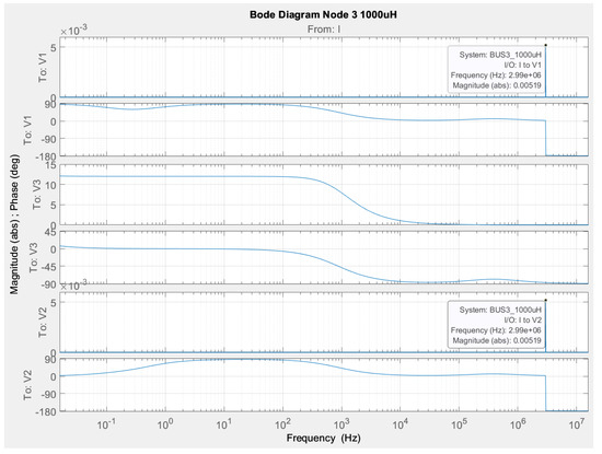
Figure 39.
Bode diagram for studying a Buck-Boost DC-DC converter, regarding Node 3 when L = 1000 µH.
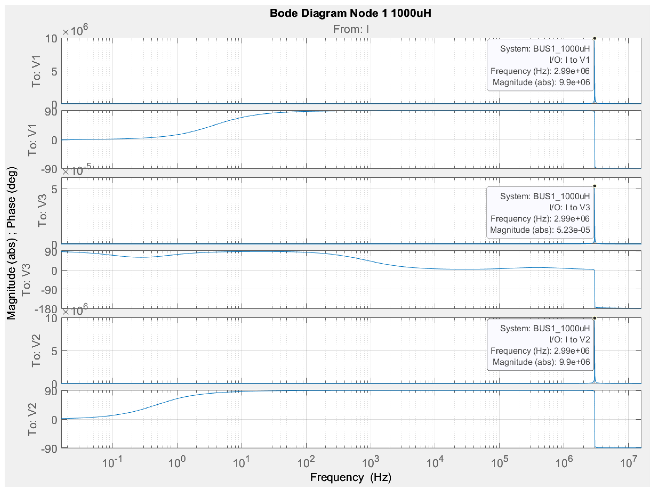
Figure 37 is a Bode plot for the same DC-DC converter, about Node 1 at an inductance value of 1000 μH. The plots show the amplitude and phase response versus frequency for different points (V1, V3, V2) at an input current (I). A resonant peak is observed around 2.99 MHz, where the amplitudes for V1 and V2 reach high values (9.9 × 10⁶), while for V3 the value is significantly lower (5.23 × 10⁻⁵). This indicates that the system exhibits a strong frequency response in this range, with V1 and V2 demonstrating the highest gain.
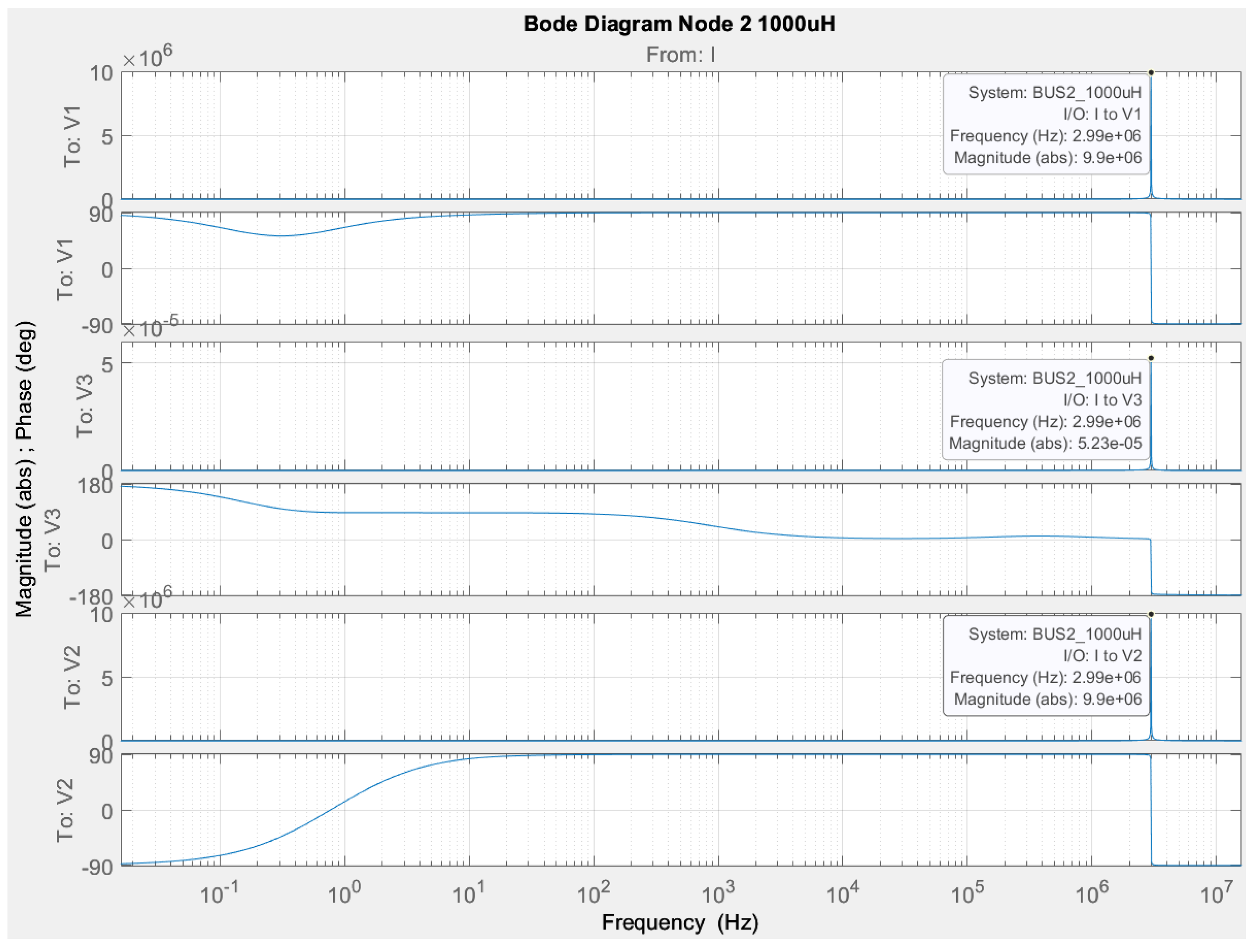
Figure 38 is a Bode plot for Node 2 with an inductance of 1000 μH. The plots show the amplitude and phase response versus frequency for different points (V1, V3, V2) at an input current (I). A resonant peak is observed at around 2.99 MHz, where the amplitudes for V1 and V2 reach high values (9.9 × 10⁶), while for V3 the value is significantly lower (5.23 × 10⁻⁵). This indicates that the system has a strong frequency response in this range, with V1 and V2 demonstrating the highest gain.
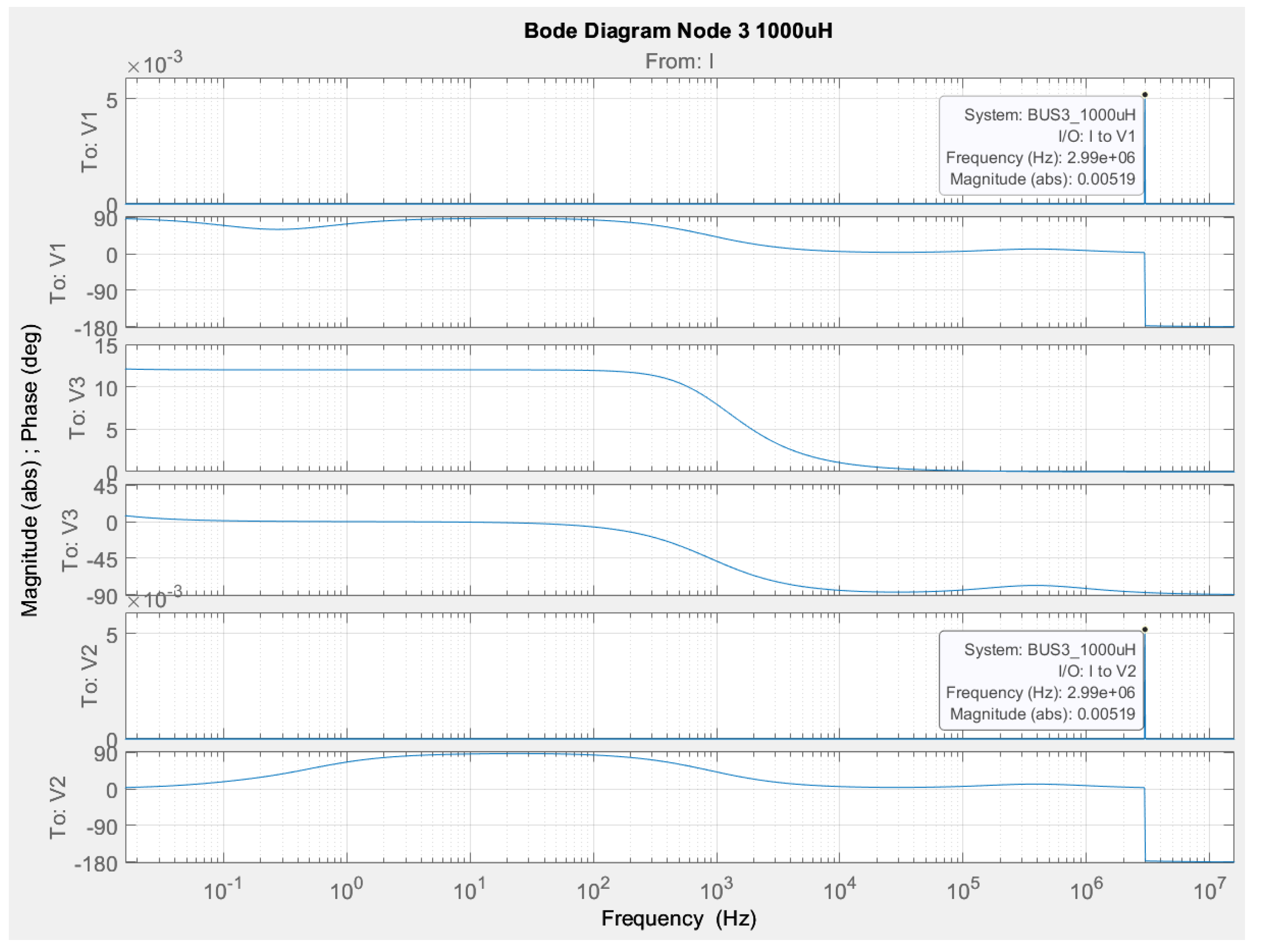
Figure 39 is a Bode plot for Node 3 with an inductance of 1000 μH. The plots show the amplitude and phase response versus frequency for different points (V1, V3, V2) at an input current (I). A frequency response is observed around 2.99 MHz, but the amplitudes for V1 and V2 are significantly lower (0.000519), suggesting that this node does not exhibit the same resonant effect as in the previous cases. The phase response shows a smooth transition depending on the frequency.
Figure 40, Figure 41 and Figure 42 show simulation results for the value of the inductance L = 1500 µH.
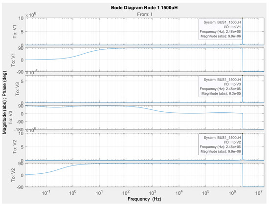
Figure 40.
Bode diagram for studying a Buck-Boost DC-DC converter, regarding Node 1 when L = 1500 µH.
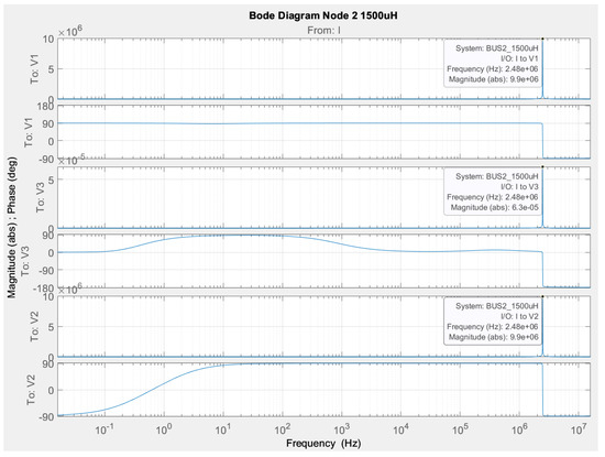
Figure 41.
Bode diagram for studying a Buck-Boost DC-DC converter, regarding Node 2 when L = 1500 µH.
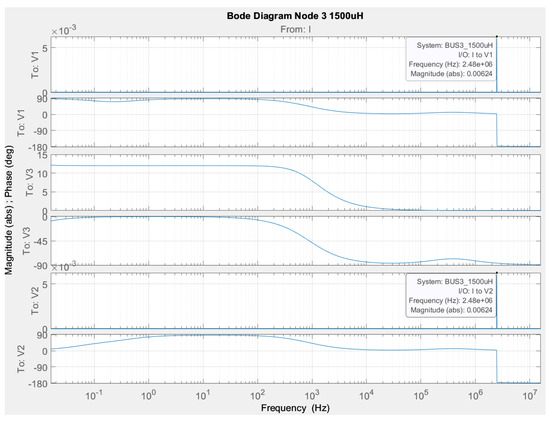
Figure 42.
Bode diagram for studying a Buck-Boost DC-DC converter, regarding Node 3 when L = 1500 µH.
Figure 40 is a Bode plot for the same DC-DC converter, regarding Node 1 with an inductance of 1500 μH. The plots show the amplitude and phase response versus frequency for different points (V1, V3, V2) at an input current (I). A resonant peak is observed around 2.48 MHz, where the amplitudes for V1 and V2 reach high values (9.9 × 10⁶), while for V3 the value is significantly lower (6.3 × 10⁻⁵). This indicates that the system exhibits a strong frequency response in this range, with V1 and V2 demonstrating the highest gain.
Figure 41 is a Bode plot for Node 2 with an inductance of 1500 μH. The plots show the amplitude and phase response versus frequency for different points (V1, V3, V2) at an input current (I). A resonant peak is observed around 2.48 MHz, where the amplitudes for V1 and V2 reach high values (9.9 × 10⁶), while for V3 the value is significantly lower (6.3 × 10⁻⁵). This indicates that the system exhibits a strong frequency response in this range, with V1 and V2 demonstrating the highest gain.
Figure 42 is a Bode plot for Node 3 with an inductance of 1500 μH. The plots show the amplitude and phase response versus frequency for different points (V1, V3, V2) at an input current (I). A frequency response is observed around 2.48 MHz, but the amplitudes for V1 and V2 are significantly lower (0.00624), suggesting that this node does not exhibit the same resonant effect as in the previous cases. The phase response shows a smooth transition depending on the frequency.
From the simulation studies presented for a Buck-Boost converter, characteristic resonance frequencies are observed that do not change in amplitude with increasing inductance value in each acting node. The only change is observed in the phases of the nodes. A characteristic plateau is observed in the response of Node 3 when a disturbance is injected into it, which decreases as frequencies of 1 × 10⁴ Hz are reached. This characteristic response is due to the parallel connected inductance and capacitance in the particular circuit [27].
5. Discussion
One of the advantages in the proposed study of DC-DC converters is that different optimization models can be applied to determine the optimal values of the inductance and the capacitor in the design, taking into account their parasitic components. Such an approach would help reduce losses in the circuit components that make up the converters.
After presenting simulation studies of the Buck, Boost and Buck-Boost converter, the following conclusions can be formulated regarding the optimal frequency range of operation with increasing value of filter inductance. For the Buck converter, it is clearly seen that the optimal frequency range of operation is in the range of 1 × 10⁴ Hz to 1 × 10⁷ Hz. As the value of the filter inductance increases, so does the influence of Node 3. These influences are noticeable due to the particular circuit solution where we observe series connection of the inductance and the load.
In the step-up converter, the presence of characteristic frequencies in the order of 1 × 10⁴ Hz and their absence in a higher frequency region in this converter is determined by a minimum threshold of the control frequency. From this conclusion, in the case of the Boost converter, it can be concluded that the optimal operating frequency should be greater than 1 × 10⁴ Hz. Also, it is noticeable that, in this specific case, the change in the filter inductance does not significantly affect the results.
A typical operating range of 1 × 10⁴ Hz to 1 × 10⁷ Hz can be observed for the Buck-Boost converter. This is a result of the circuit design of the converter, where the inductance is in parallel with the capacitance and the load. For loads with a higher power value, the influence of the filter inductance should be significantly reduced. This is due to the principle of operation of the scheme: when switch is off, the energy stored in the inductance is stored in the load and part of it is stored in the capacitor.
In [28], the stability of the devices in stand-alone and cascaded operation, based on the application of a discrete-time map model, was investigated sequentially. The mechanism for studying the instability of the converter is formed on the basis of a description of the variations of the parameters of the power circuits, and the limits of stability are determined. The results show that the obtained limits of stability of the circuit parameters of the device are different in stand-alone operation and in cascade mode, because the influence of the ripples on the input and output currents and voltages between the individual converters is observed. In this regard, the proposed stability research approach is very suitable for application in cascade power converters, and it is one of the directions for future research development.
6. Conclusions
The wide application of power electronic converters is one of the main reasons why many scientists are researching their working principle and improving their efficiency. From the presented literature review, it can be seen that electronic converters are necessary renewable sources of electricity, in the control of engines, in the construction of charging stations for electric vehicles, in the design of autonomous power networks, and also in the storage of electricity in various elements for storage, such as batteries and supercapacitors, etc. Of course, finding a power converter for a specific application requires choosing a specific topology and control method. Also, it is necessary to select an appropriate design methodology that meets the requirements. Solving an optimization task in the design could facilitate the selection of appropriate parameters of the components, increase the efficiency of the converter, reduce losses, and determine a specific frequency range of operation to reduce the occurrence of resonance processes.
In this paper, a simulation study of three specific DC-DC converters that can be used for different applications, depending on the input and output voltage requirements, was conducted. Three models implemented with substitution schemes for the circuit elements were presented. Mathematical models were implemented in MATLAB/Simulink. The influence of changing the filter inductance with different values was evaluated. A standard design methodology and similar parameters of the circuit elements were used in the different converters. The purpose of the realized study was to determine a suitable operating range depending on the operating frequency of the converter. The proposed research is suitable in the design of the different types of DC-DC converters. Consideration of the occurrence of resonance in the standard methodologies used can be helpful in selecting an appropriate converter operating frequency. Also, a significant influence was observed when varying the filter inductance and coupling and with the output capacitance of the particular circuit.
The study of various parameters in the design of power electronic converters is one way to determine optimal control, to increase efficiency, and to reduce losses. The application of different methodologies and new approaches would greatly aid in the realization of these goals. Examining the different DC-DC converters and the effect of resonance at certain input disturbances could also help in choosing the right converter for the different application. An interesting study that could be conducted in future developments is one that determines, in addition to the change in the filter inductance, how a simultaneous change in the value of the output capacitance would affect the selection of an appropriate duty cycle for the various converters.
Author Contributions
N.H., P.S. and G.V. were involved in the full process of producing this paper, including conceptualization, methodology, modeling, validation, visualization, and preparation of the manuscript. All authors have read and agreed to the published version of the manuscript.
Funding
This research was funded by Bulgarian National Scientific Fund, grant number KП-06-H57/7/16.11.2021, and the APC was funded by KП-06-H57/7/16.11.2021.
Institutional Review Board Statement
Not applicable.
Informed Consent Statement
Not applicable.
Data Availability Statement
Data are contained within the article.
Acknowledgments
This research was carried out within the framework of the project “Artificial Intelligence-Based modeling, design, control and operation of power electronic devices and sys-tems”, KП-06-H57/7/16.11.2021, Bulgarian National Scientific Fund.
Conflicts of Interest
The authors declare no conflicts of interest.
References
- Górecki, P.; Górecki, K. Methods of Fast Analysis of DC–DC Converters—A Review. Electronics 2021, 10, 2920. [Google Scholar] [CrossRef]
- Camail, P.; Allard, B.; Darnon, M.; Joubert, C.; Martin, C.; Trovão, J.P.F. Overview of DC/DC Converters for Concentrating Photovoltaics (CPVs). Energies 2023, 16, 7162. [Google Scholar] [CrossRef]
- Lopa, S.A.; Hossain, S.; Hasan, M.K.; Chakraborty, T.K. Design and simulation of DC-DC converters. Int. Res. J. Eng. Technol. (IRJET) 2016, 3, 63–70. [Google Scholar]
- Available online: https://standards.cencenelec.eu/dyn/www/f?p=205:105:0::::: (accessed on 27 October 2024).
- Wang, X.; Frede, B. Harmonic stability in power electronic-based power systems: Concept, modeling, and analysis. IEEE Trans. Smart Grid 2018, 10, 2858–2870. [Google Scholar] [CrossRef]
- Tokic, A.; Jukan, A.; Suljkanovic, V. Modelling of Low Power Electronic Loads in Harmonic Analysis. IFAC-PapersOnLine 2015, 48, 675–676. [Google Scholar] [CrossRef]
- Kou, L.; Peng, Y.; Ji, K.; Zhu, L.; Ji, F.; Liu, D. Harmonic Stability Analysis and Damping Strategy for DC system of MMC-HVDC Across Wide Frequency Range. In Proceedings of the 2021 International Conference on Power System Technology: Carbon Neutrality and New Type of Power System, POWERCON 2021, Haikou, China, 8–9 December 2021; pp. 1645–1651. [Google Scholar] [CrossRef]
- Zhang, H.; Jing, M.; Liu, W.; Dong, D. Multiple-Harmonic Modeling and Analysis of Single-Inductor Dual-Output Buck DC–DC Converters. IEEE J. Emerg. Sel. Top. Power Electron. 2020, 8, 3260–3271. [Google Scholar] [CrossRef]
- Ji, K.; Tang, G.; Yang, J.; Li, Y.; Liu, D. Harmonic Stability Analysis of MMC-Based DC System Using DC Impedance Model. IEEE J. Emerg. Sel. Top. Power Electron. 2020, 8, 1152–1163. [Google Scholar] [CrossRef]
- Li, P.; Wang, Y.; Li, X.; Yue, B.; Li, R.; Feng, B. DC Impedance Modeling and Design-Oriented Harmonic Stability Analysis of MMC-PCCF-Based HVDC System. IEEE Trans. Power Electron. 2022, 37, 4301–4319. [Google Scholar] [CrossRef]
- Wang, Y.; Duan, G.; Yu, J.; Yue, W.; Ning, J.; Liu, B. Harmonic Analysis of Sliding-Mode-Controlled Buck Converters Imposed by Unmodeled Dynamics of Hall Sensor. Energies 2023, 16, 6124. [Google Scholar] [CrossRef]
- Rauf, A.M.; Abdel-Monem, M.; Geury, T.; Hegazy, O. A Review on Multilevel Converters for Efficient Integration of Battery Systems in Stationary Applications. Energies 2023, 16, 4133. [Google Scholar] [CrossRef]
- Xie, L.; Wan, D. Modeling and Harmonic Analysis of a Fractional-Order Zeta Converter. Energies 2023, 16, 3969. [Google Scholar] [CrossRef]
- Park, B.; Lee, J.; Yoo, H.; Jang, G. Harmonic Mitigation Using Passive Harmonic Filters: Case Study in a Steel Mill Power System. Energies 2021, 14, 2278. [Google Scholar] [CrossRef]
- Mei, N.; Yin, S.; Wang, Y.; Li, Z.; Li, P.; Liu, Y.; Yue, B.; Li, Z. Small Signal Modeling and Stability Analysis of Modular Multilevel Converter Based on Harmonic State-Space Model. Energies 2020, 13, 1056. [Google Scholar] [CrossRef]
- Gsous, O.; Rizk, R.; Barbón, A.; Georgious, R. Review of DC-DC Partial Power Converter Configurations and Topologies. Energies 2024, 17, 1496. [Google Scholar] [CrossRef]
- Amar, N.; Ziv, A.; Strajnikov, P.; Kuperman, A.; Aharon, I. Topological Overview of Auxiliary Source Circuits for Grid-Tied Converters. Machines 2023, 11, 171. [Google Scholar] [CrossRef]
- Granata, S.; Di Benedetto, M.; Terlizzi, C.; Leuzzi, R.; Bifaretti, S.; Zanchetta, P. Power Electronics Converters for the Internet of Energy: A Review. Energies 2022, 15, 2604. [Google Scholar] [CrossRef]
- Aragon-Aviles, S.; Trivedi, A.; Williamson, S.S. Smart Power Electronics–Based Solutions to Interface Solar-Photovoltaics (PV), Smart Grid, and Electrified Transportation: State-of-the-Art and Future Prospects. Appl. Sci. 2020, 10, 4988. [Google Scholar] [CrossRef]
- Vyapari, S. Design Oriented Steady State Analysis of Series and Parallel Resonant Converters. In Proceedings of the 2022 IEEE International Conference on Industrial Technology (ICIT), Shanghai, China, 22–25 August 2022; pp. 1–6. [Google Scholar] [CrossRef]
- El Aroudi, A.; Giaouris, D.; Iu HH, C.; Hiskens, I.A. A Review on Stability Analysis Methods for Switching Mode Power Converters. IEEE J. Emerg. Sel. Top. Circuits Syst. 2015, 5, 302–315. [Google Scholar] [CrossRef]
- Moschopoulos, G. DC-DC Converter Topologies: Basic to Advanced; Wiley-IEEE Press: Hoboken, NJ, USA, 2023; ISBN 978-1-119-61242-1. [Google Scholar]
- Mahmud, T.; Gao, H. A Comprehensive Review on Matrix-Integrated Single-Stage Isolated MF/HF Converters. Electronics 2024, 13, 237. [Google Scholar] [CrossRef]
- Khan, M.U.; Murtaza, A.F.; Noman, A.M.; Sher, H.A.; Zafar, M. State-Space Modeling, Design, and Analysis of the DC-DC Converters for PV Application: A Review. Sustainability 2024, 16, 202. [Google Scholar] [CrossRef]
- Sah, B.; Kumar, G.V.E.S. A comparative study of different MPPT techniques using different dc-dc converters in a standalone PV system. In Proceedings of the 2016 IEEE Region 10 Conference (TENCON), Singapore, 22–25 November 2016; pp. 1690–1695. [Google Scholar]
- Zhang, W.; Tan, X.; Wang, K.; Li, T.; Chen, J. Design for boost DC-DC converter controller based on state-space average method. Integr. Ferroelectr. 2016, 172, 152–159. [Google Scholar] [CrossRef]
- Molina-Santana, E.; Gonzalez-Montañez, F.; Liceaga-Castro, J.U.; Jimenez-Mondragon, V.M.; Siller-Alcala, I. Modeling and Control of a DC-DC Buck–Boost Converter with Non-Linear Power Inductor Operating in Saturation Region Considering Electrical Losses. Mathematics 2023, 11, 4617. [Google Scholar] [CrossRef]
- Zhang, X.; Wang, T.; Bao, H.; Hu, Y.; Bao, B. Stability Effect of Load Converter on Source Converter in a Cascaded Buck Converter. IEEE Trans. Power Electron. 2023, 38, 604–618. [Google Scholar] [CrossRef]

Disclaimer/Publisher’s Note: The statements, opinions and data contained in all publications are solely those of the individual author(s) and contributor(s) and not of MDPI and/or the editor(s). MDPI and/or the editor(s) disclaim responsibility for any injury to people or property resulting from any ideas, methods, instructions or products referred to in the content. |
© 2025 by the authors. Licensee MDPI, Basel, Switzerland. This article is an open access article distributed under the terms and conditions of the Creative Commons Attribution (CC BY) license (https://creativecommons.org/licenses/by/4.0/).