Article

Highly Adaptive Reconfigurable Receiver Front-End for 5G and Satellite Applications

1
Communication and Space Systems Engineering Research Team, Manchester Metropolitan University, Manchester M1 5GD, UK
2
Department of Communication and Informatics Engineering, Al-Farqadein University College, Basrah 61004, Iraq
*
Author to whom correspondence should be addressed.
Technologies 2025, 13(4), 124; https://doi.org/10.3390/technologies13040124
Submission received: 18 February 2025 / Revised: 15 March 2025 / Accepted: 18 March 2025 / Published: 22 March 2025

Abstract

:
The deployment of fifth-generation (5G) and beyond-5G wireless communication systems necessitates advanced transceiver architectures to support high data rates, spectrum efficiency, and energy-efficient designs. This paper presents a highly adaptive reconfigurable receiver front-end (HARRF) designed for 5G and satellite applications, integrating a switchable low noise amplifier (LNA) and a single pole double throw (SPDT) switch. The HARRF architecture supports both X-band (8–12 GHz) and K/Ka-band (23–28 GHz) operations, enabling seamless adaptation between radar, satellite communication, and millimeter-wave (mmWave) 5G applications. The proposed receiver front-end employs a 0.15 μ m pseudomorphic high electron mobility transistor (pHEMT) process, optimised through a three-stage cascaded LNA topology. A switched-tuned matching network is utilised to achieve reconfigurability between X-band and K/Ka-band. Performance evaluations indicate that the X-band LNA achieves a gain of 23–27 dB with a noise figure below 7 dB, whereas the K/Ka-band LNA provides 23–27 dB gain with a noise figure ranging from 2.3–2.6 dB. The SPDT switch exhibits low insertion loss and high isolation, ensuring minimal signal degradation across operational bands. Network analysis and scattering parameter extractions were conducted using advanced design system (ADS) simulations, demonstrating superior return loss, power efficiency, and impedance matching. Comparative analysis with state-of-the-art designs shows that the proposed HARRF outperforms existing solutions in terms of reconfigurability, stability, and wideband operation. The results validate the feasibility of the proposed reconfigurable RF front-end in enabling efficient spectrum utilisation and energy-efficient transceiver systems for next-generation communication networks.

1. Introduction

The exponential growth in data-intensive applications, coupled with the drive towards fifth-generation (5G) and beyond-5G (B5G) communication systems, has placed renewed emphasis on developing reconfigurable front-end architectures that are capable of high data rates, enhanced spectral efficiency, and energy-saving functionalities [1,2,3]. In particular, 5G networks are expected to address an expanding user base as well as support diverse use cases ranging from Internet-of-Things (IoT) deployments to mission-critical applications such as autonomous vehicles, telemedicine, and high-throughput satellite communication links [4,5,6]. Beyond-5G research, moreover, points towards utilisation of wider bandwidths in the millimeter-wave (mmWave) frequency bands and beyond, further increasing design complexity and performance demands.
Non-Terrestrial Networks (NTNs) have become essential for global connection, closing the digital divide and providing dependable communication in rural and underserved areas [7]. The amalgamation of Non-Terrestrial Networks (NTNs) with terrestrial networks aims to ensure uninterrupted service and worldwide coverage, hence advancing the scope of wireless communication technologies [7]. This integration, however, presents considerable technological problems, especially with signal processing, adaptive resource allocation, and radio front-end architecture. Recent advancements in software-defined radio (SDR) architectures have been pivotal in overcoming these challenges by facilitating the flexible reconfiguration of transceivers to accommodate diverse channel conditions, network topologies, and regulatory constraints [8,9]. Moreover, SDR-based solutions provide real-time spectrum detection, dynamic frequency selection, and cognitive radio capabilities, thereby improving spectral efficiency and reducing interference.
Contemporary wireless systems increasingly require multi-band functionality, utilising many frequency bands to optimise coverage, capacity, and propagation attributes [10,11,12]. Lower frequency bands (under 6 GHz) offer broader coverage with less route losses, rendering them appropriate for broad-area connection. In contrast, mmWave bands (24–40 GHz and beyond) provide significantly elevated data speeds by using extensive, underexploited spectrum resources. The presence of several wireless protocols, including as 4G, 5G, Wi-Fi, and NTN connections, requires highly adaptable front-end designs that can rapidly transition across frequency bands while reducing hardware complexity, power consumption, and system overhead [6,13].
Reconfigurable receiver front-ends are of particular interest due to their ability to dynamically adjust key performance metrics such as gain, bandwidth, and noise figure based on real-time link requirements. Such adaptability is essential for heterogeneous networks supporting diverse applications, from massive Machine-Type Communications (mMTC) to ultra-reliable low-latency communication (URLLC) [14]. Reconfigurable architectures further enhance interference suppression and spectrum efficiency by incorporating advanced techniques such as adaptive beamforming, frequency-agile filters, and hybrid analogue-digital signal processing [5].
Within an RF receiver chain, the low noise amplifier (LNA) is a fundamental component that significantly influences system sensitivity and overall noise performance [15,16]. Achieving an ultra-low noise figure (NF) is particularly crucial in high-frequency bands such as mmWave, where high propagation losses and atmospheric absorption necessitate stringent link budget optimisations [12]. Complementing the LNA, RF switches play a critical role in routing signals across different frequency bands and enabling transmit-receive path reconfiguration. Single-pole double-throw (SPDT) switches are commonly employed due to their ability to provide low insertion loss, high isolation, and fast switching speeds [17]. However, integration challenges, including impedance mismatches and parasitic effects, must be carefully mitigated to ensure optimal system performance.
To address these challenges, recent research has explored advanced semiconductor technologies, including complementary metal-oxide-semiconductor (CMOS), silicon-germanium (SiGe) BiCMOS, and gallium arsenide (GaAs) pseudomorphic high electron mobility transistor (pHEMT) processes. GaAs pHEMT technology, in particular, offers superior high-frequency performance with minimal noise degradation, making it a strong candidate for wideband and mmWave applications [18]. Several reconfigurable LNA topologies have been proposed, incorporating switched matching networks, tunable resonators, and multi-stage amplification to optimize trade-offs between gain, linearity, noise figure, and power efficiency [2,3].
In light of these advancements, this paper presents a novel highly adaptive reconfigurable receiver front-end (HARRF) designed to support both 5G and NTN applications through a unified hardware platform. The proposed front-end integrates a switchable LNA and an SPDT switch, enabling seamless reconfiguration between X-band (8–12 GHz) and K/Ka-band (23–28 GHz). This dynamic frequency agility is particularly beneficial for satellite communication, radar sensing, and mmWave 5G applications, where stringent performance requirements necessitate flexible hardware architectures.
The chosen 0.15 μ m GaAs pHEMT process offers an optimal combination of wideband operation, low noise, and high gain, ensuring robust performance in challenging RF environments [15,16]. The LNA employs a three-stage cascaded topology with frequency-selective feedback networks to achieve optimal gain flatness and noise performance across both operational bands. Additionally, a switched-tuned matching network is implemented to facilitate dynamic frequency reconfiguration while minimising component overhead and insertion losses. The SPDT switch is designed with an emphasis on achieving minimal signal degradation, high port isolation, and rapid switching transitions, ensuring reliable operation in frequency-diverse environments.
This study demonstrates the feasibility of reconfigurable RF front-end design through the implementation of a switched-tuned matching technique, enabling seamless frequency transitions between X-band and K-band. Section 2.1 provides a comprehensive overview of the highly adaptive reconfigurable receiver front-end (HARRF) architecture for 5G and satellite applications. Section 3 elaborates on the key design considerations for the switchable receiver front-end, followed by an in-depth discussion of active device technology and S-parameter extraction in Section 4. Section 5 presents the detailed design and analysis of the HARRF LNA, while Section 6 focuses on the SPDT switch design and optimisation. Section 7 discusses the experimental results, including the performance evaluation of the wideband SPDT switch and the reconfigurable front-end. Finally, Section 8 concludes the paper, summarising key contributions and potential future research directions.

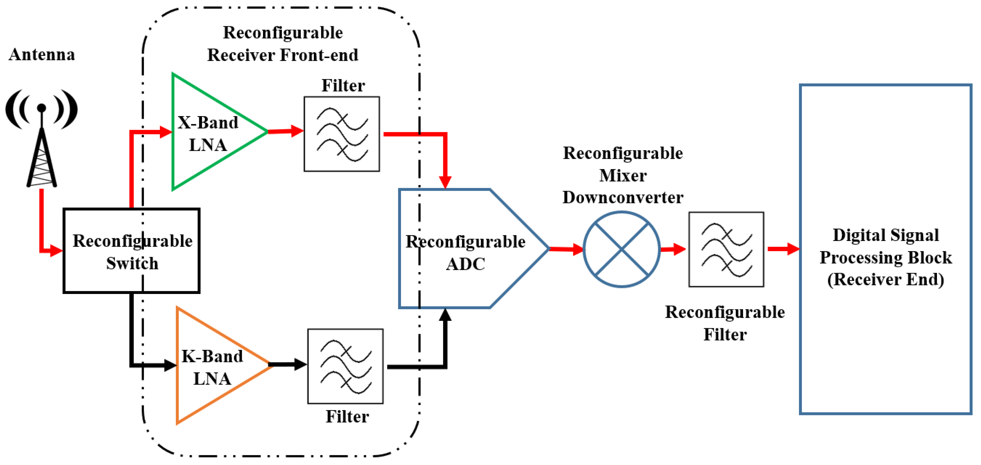
2. Highly Adaptive Reconfigurable Receiver Front-End (HARRF) for 5G and Satellite Applications

A highly adaptive reconfigurable receiver front-end (HARRF) for 5G and satellite applications is presented. The proposed design utilizes a Single-Pole Double-Throw (SPDT) switch to toggle its functionality between X-band frequencies, primarily for radar and satellite communication, and K/Ka-band frequencies, which support wideband switchable applications, particularly for millimeter-wave (mmWave) 5G communications in Frequency Range 2 (FR2).

2.1. Conceptual Design Objectives

The design of the switchable receiver front-end operating at X-band (8–12 GHz) and K/Ka-band (18–40 GHz) frequencies must consider key objectives such as:
  • High Linearity: Ensuring minimal distortion under high-power signal conditions.
  • Low Noise Figure (NF): Optimising the sensitivity of the receiver.
  • Adequate Gain: Maintaining sufficient signal amplification while minimising losses.
  • Efficient Switching Mechanism: Seamless transition between X-band and K/Ka-band with minimal insertion loss.
  • Wideband Operation: Supporting mmWave 5G FR2 applications with bandwidth flexibility.

2.2. Design Parameter Definitions

To achieve these objectives, the following parameters are defined:
  • Noise Figure (NF):
The NF of the receiver front-end is given by:
N F = 10 log 10 1 + F 1 G ( dB )
where F is the noise factor and G is the system gain.
  • Gain ( G T ):
The total gain of the receiver front-end is calculated using:
G T = G 1 G 2 G 3 G N
where G n represents the individual stage gain.
  • Linearity and Third-Order Intercept Point (IP3):
The overall IP3 of cascaded stages is approximated as:
1 I P 3 t o t a l = 1 I P 3 1 + G 1 I P 3 2 + G 1 G 2 I P 3 3 + + G 1 G 2 G N 1 I P 3 N

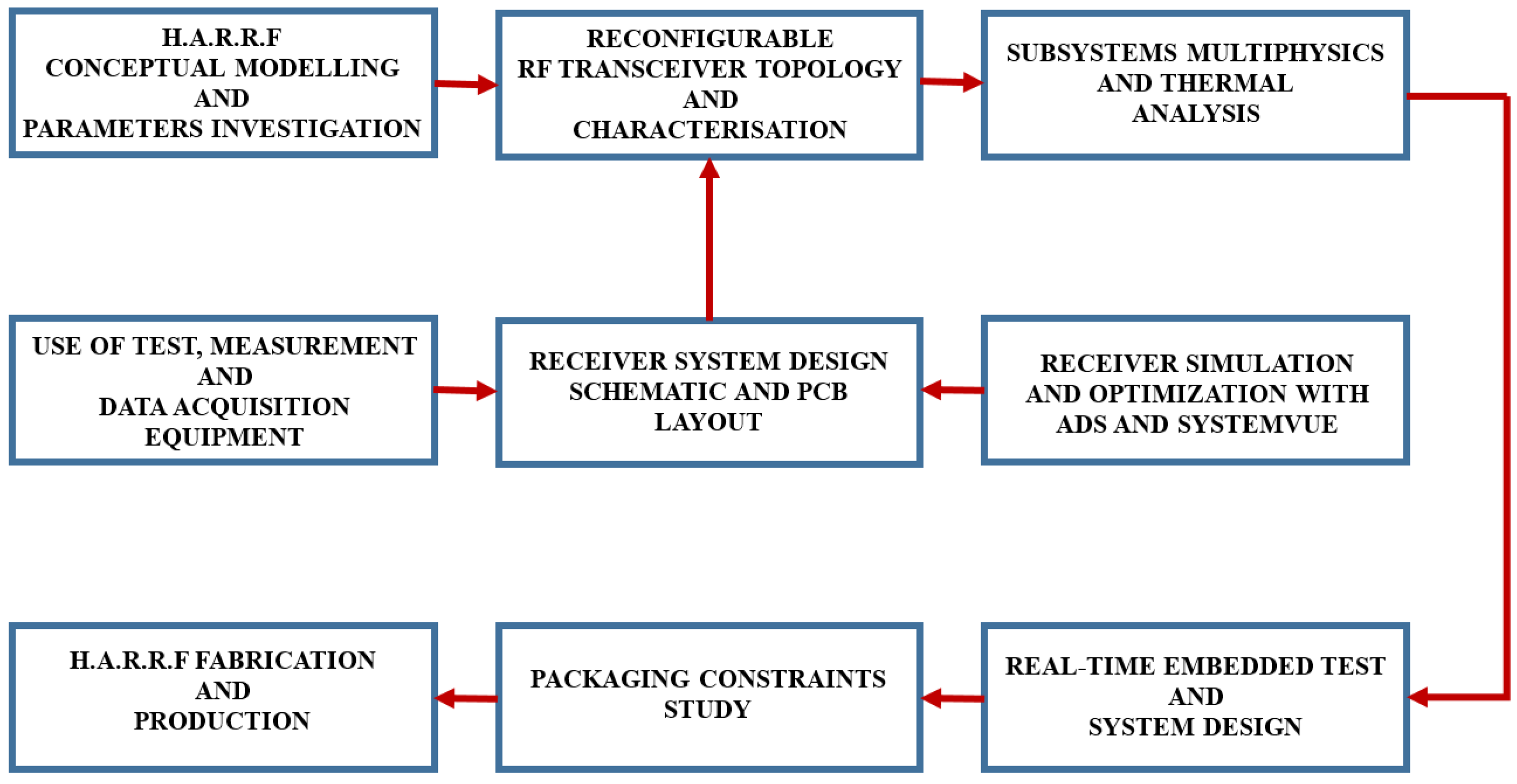
2.3. Design Process Flow

The overall design process of the HARRF involves multiple stages, including requirement specification, circuit design, optimisation, and validation. Figure 1 illustrates the design process flow.

3. Switchable Receiver Front-End Architecture: HARRF LNA and SPDT Integration

The design of the switchable wideband receiver frontend, incorporating the Low Noise Amplifier (LNA) and Single Pole Double Throw (SPDT) Switch, involves generating multiple design scenarios to optimise the performance of the communication infrastructure for both 5G and satellite applications. The cascade topology is selected for the LNA due to its superior gain performance and impedance matching compared to common-source and common-gate configurations. This ensures compliance with low-noise performance requirements across multiple wireless standards spanning a wide frequency spectrum.
Figure 2 shows the suggested receiver frontend module design for HARRF 5G and Satellite receiver systems. The system uses two LNAs to collect X-band and K/Ka-band signals. Selecting the frequency band uses an SPDT switch. Transmission lines connect the SPDT switch to the LNAs, decreasing chip footprint. This receiver frontend design switches between X-band and K/Ka-band modes using a voltage-driven SPDT switch. The SPDT switch receives and routes the incoming RF signal as the primary driving stage.

3.1. Mathematical Model of the Receiver Frontend

The total noise figure ( F t o t a l ) of the cascaded system, incorporating the SPDT switch and LNAs, is derived using Friis’ equation:
F t o t a l = F 1 + F 2 1 G 1 + F 3 1 G 1 G 2 + + F n 1 G 1 G 2 G n 1 ,
where:
-
F i represents the noise figure of each stage,
-
G i denotes the gain of the preceding stages.
For a two-stage receiver frontend comprising an SPDT switch and an LNA, this equation simplifies to:
F t o t a l = F S P D T + F L N A 1 G S P D T ,
where F S P D T and F L N A are the noise figures of the SPDT switch and the LNA, respectively, while G S P D T represents the gain of the SPDT switch.
The input impedance ( Z i n ) of the cascaded system is expressed as:
Z i n = Z 0 1 + Γ i n 1 Γ i n ,
where Z 0 is the characteristic impedance (typically 50 Ω ), and Γ i n is the input reflection coefficient defined as:
Γ i n = Z L Z 0 Z L + Z 0 .
The gain of the cascaded system is given by:
G t o t a l = G S P D T · G L N A .
The power delivered to the receiver frontend is calculated using:
P i n = f 1 f 2 S 21 ( f ) d f ,
where S 21 ( f ) represents the forward transmission coefficient of the system over the frequency range f 1 to f 2 .
The operation of the SPDT switch is governed by a voltage-controlled mechanism where the transfer function can be expressed as:
V o u t = G X V i n , if switch in X - band mode , G K / K a V i n , if switch in K / Ka - band mode ,
where G X and G K / K a represent the gain factors for the respective frequency bands.

3.2. Transmission Line Integration

To optimise integration, the transmission line impedance transformation is given by:
Z T L = Z 0 Z L N A + j Z 0 tan ( β l ) Z 0 + j Z L N A tan ( β l ) ,
where:
-
Z T L is the transmission line impedance,
-
β is the propagation constant,
-
l is the transmission line length.
The phase shift introduced by the transmission lines is given by:
ϕ = β l = 2 π λ l ,
where λ is the wavelength of the operating frequency.

3.3. Impedance Matching Between the Switch and the LNA

The incorporation of the Single-Pole Double-Throw (SPDT) switch with the Low Noise Amplifier (LNA) in the Highly Adaptive Reconfigurable Receiver Front-End (HARRF) design entails significant impedance matching challenges. Efficient impedance matching between these two components is crucial to reduce reflection losses, improve power transmission, and guarantee excellent noise performance throughout the operational frequency ranges. This section offers a comprehensive analysis of the impedance matching techniques utilised between the SPDT switch and the LNA, encompassing theoretical aspects, practical design approaches, and performance compromises.
The impedance disparity between the SPDT switch and the LNA may result in power losses and signal deterioration. The essential criterion for optimal power transmission is defined by the conjugate matching condition:
Z L N A * = Z S w i t c h ,
where Z L N A * is the complex conjugate of the LNA input impedance, and Z S w i t c h is the output impedance of the SPDT switch.
At microwave and millimeter-wave frequencies, the impedance observed at the input of the LNA is affected by both the nominal switch impedance and parasitic factors, including switch capacitance, substrate losses, and transmission line discontinuities. The comprehensive impedance transformation can be expressed as:
Z i n = Z 0 1 + Γ i n 1 Γ i n ,
where Z 0 is the characteristic impedance (typically 50 Ω ) and Γ i n is the input reflection coefficient.
In cascaded networks, such as the switch-LNA combination, the impedance matching condition is determined by the transmission and reflection coefficients at the interface. The reflection coefficient at the input of the LNA resulting from the SPDT switch can be expressed as:
Γ L N A = Z L N A Z S w i t c h Z L N A + Z S w i t c h .
For ideal matching, Γ L N A should be minimised to ensure negligible reflection.
To comprehensively analyse the impedance mismatch, we consider the total voltage transfer function across the cascaded network, expressed as:
H ( f ) = V o u t V i n = Z L N A Z L N A + Z S w i t c h + j ω L + 1 j ω C ,
where L and C represent the parasitic inductance and capacitance of the transmission line interconnecting the switch and the LNA. The reflection coefficient, incorporating transmission line effects, is given by:
Γ ( f ) = Z L N A Z S w i t c h j X T L Z L N A + Z S w i t c h + j X T L ,
where X T L is the reactance of the transmission line connecting the two elements, given by:
X T L = Z 0 tan ( β l ) ,
and β is the propagation constant.
To mitigate impedance mismatch effects, a multi-stage matching network is employed to ensure efficient signal transfer. The impedance transformation ratio is determined as:
T m a t c h = Z L N A Z S w i t c h ,
and the required reactance values for an L-section matching network can be derived from:
X L = R L N A ( R S w i t c h R L N A ) ,
X C = R L N A R S w i t c h X L .
For a broadband Pi-matching network, the impedance transformation function is given by:
Z i n = Z L N A Z S w i t c h + j ω L 1 j ω C Z S w i t c h + j ω L .
Using a quarter-wave transformer, the impedance transformation equation simplifies to:
Z i n = Z 0 2 Z o u t ,
where Z o u t is the transformed impedance at the LNA input.

3.4. Impact on Noise Figure and Gain

Impedance mismatch can significantly degrade the overall noise figure and gain performance of the receiver front-end. Using Friis’ formula, the total noise figure incorporating mismatch losses can be represented as:
N F t o t a l = N F S w i t c h + N F L N A 1 G S w i t c h + 10 log 10 ( 1 | Γ L N A | 2 ) ,
where the last term accounts for the reflection loss due to impedance mismatch.
Similarly, the cascaded gain of the receiver front-end considering mismatch reflections is given by:
G t o t a l = G S w i t c h × G L N A × ( 1 | Γ L N A | 2 ) × 1 | S 11 | 2 | S 21 | 2 ,
where S 11 and S 21 represent the scattering parameters of the SPDT switch.
Simulated results confirm that the designed matching network minimizes impedance discontinuities, ensuring optimal signal power transfer between the SPDT switch and LNA.

4. Active Device Technology S-Parameter Extraction

The selection of the appropriate process technology is crucial, taking into account the unique operating requirements of the intended application. In order to accomplish a successful design, it is necessary to pick a mix of active devices (such as diodes and transistors) and passive devices (such as inductors and capacitors), using a well-defined process technology. This selection should be made to satisfy the design goals and expected performance level of the system. At lower frequencies, the active device components are characterised using impedance (Z) and admittance (Y) parameters, defined as:
Z = V I , Y = 1 Z = I V
These parameters provide a linear connection between the input and output voltages and currents. However, in the context of microwave frequencies, power measurements are conducted using scattering parameters (S-parameters), which analyse the distribution of a signal across different ports of the microwave network. The reflection and transmission properties of a two-port network are given as:
S 11 = V 1 V 1 + , S 21 = V 2 V 1 + , S 12 = V 1 V 2 + , S 22 = V 2 V 2 +
where V i + and V i represent the incident and reflected voltage waves at port i.
The insertion loss of transmission lines decreases when using substrates with higher resistivity, as the impact of substrate losses and the quality factor of matching networks are key performance indicators.

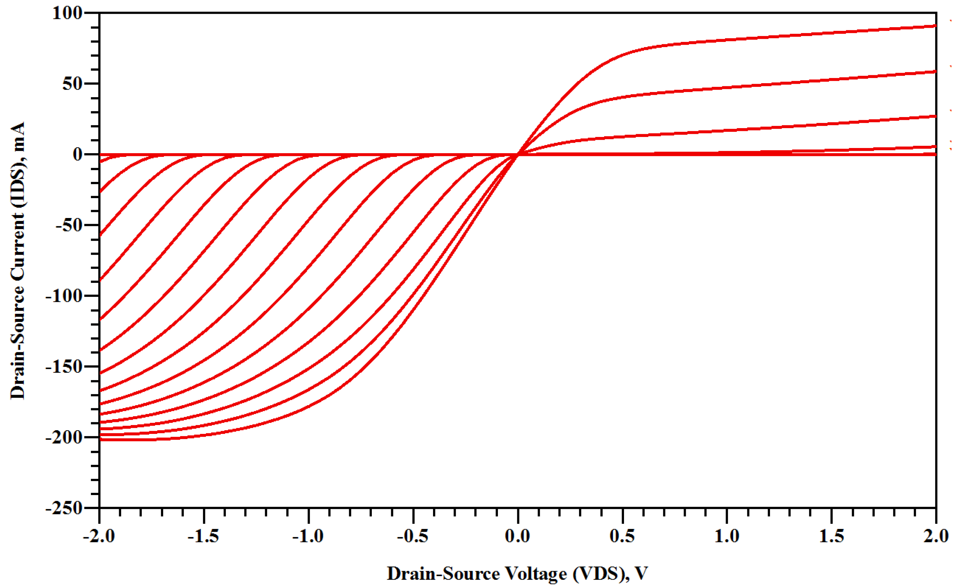
4.1. I-V Characteristics of pHEMT Devices

DC and RF test simulations are carried out under a variety of bias situations to ascertain the operating point of the transistor. This is done to gain an understanding of the non-linear features of the pseudomorphic high electron mobility transistor (pHEMT) active device via S-parameter extraction. Figure 3 displays the I-V characteristics of Indium Gallium Arsenide (InGaAs) pHEMTs at various biasing points for a 2 × 50   μ m InGaAs pHEMT while Figure 4 displays the I-V characteristics of Indium Gallium Arsenide (InGaAs) pHEMTs at various biasing points for a 4 × 50   μ m InGaAs pHEMT
The drain current ( I d s ) is plotted versus the drain-source voltage ( V d s ), where the operating point is chosen at V d s = 2   V , V g s = 0.3   V , and I d s = 0.021   A . The power dissipation for a three-stage low-noise amplifier (LNA) design is determined by:
P d i s s = V d s I d s
where P d i s s < 0.14   W .

4.2. Transconductance Characteristics

Figure 5 and Figure 6 display the transconductance characteristics of two different sizes of InGaAs pHEMTs, 2 × 50 μ m and 4 × 50 μ m , respectively. The transconductance g m is defined as:
g m = I d s V g s
From Figure 5, the transconductance value obtained is 81 m S at V d s = 2   V , V g s = 0.3   V , and I d s = 0.021   A .

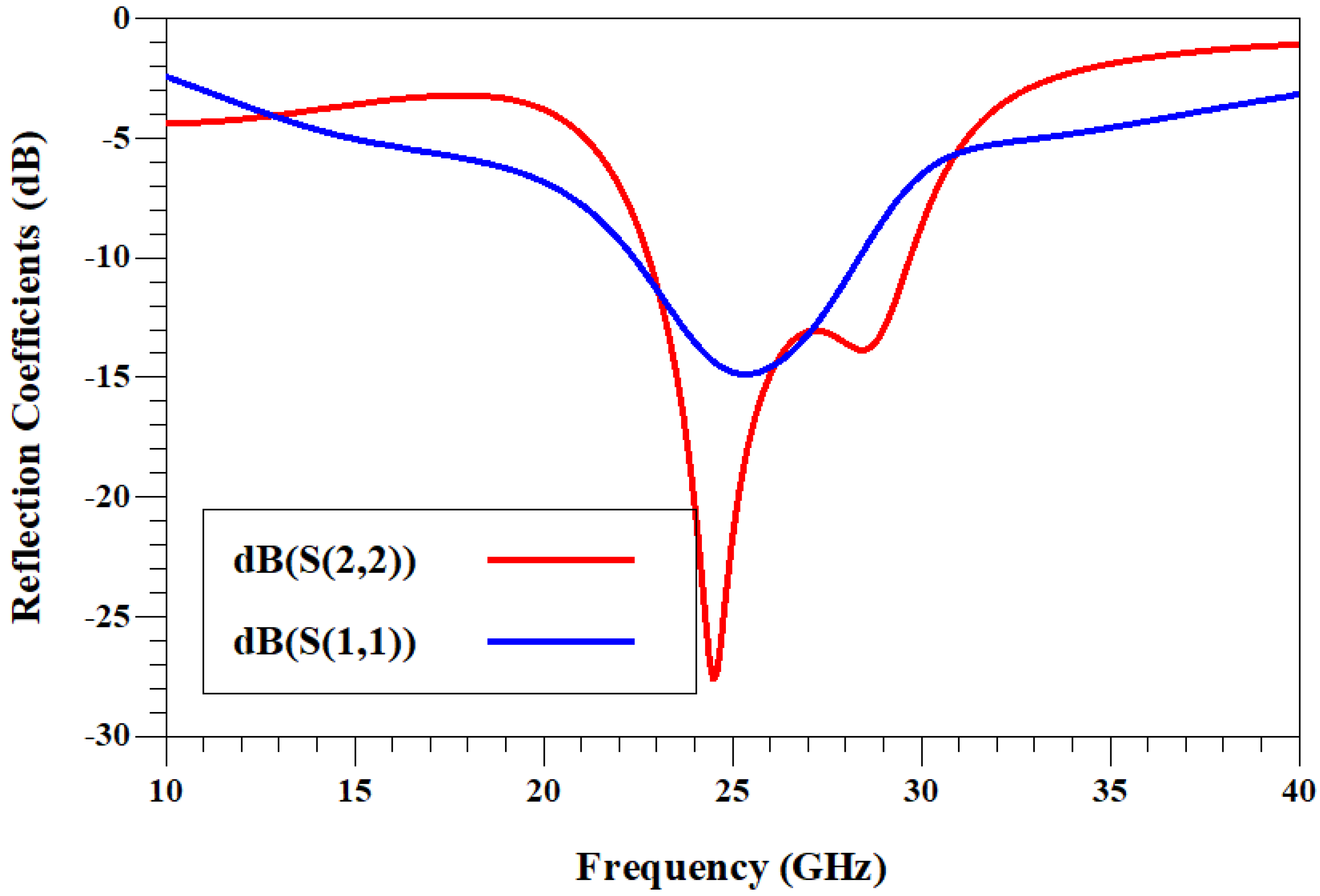
4.3. Reflection Coefficient and Matching Conditions

The load reflection coefficient, Γ o p t , plays a crucial role in determining the efficiency of power transfer and noise performance of a pHEMT device. This is distinct from the conjugate reflection coefficient of the input return loss, S 11 . The optimal power transfer occurs when:
Γ o p t = Z L Z 0 Z L + Z 0
where Z L is the load impedance and Z 0 is the characteristic impedance of the system.
By carefully selecting the appropriate transistor, the difference between Γ o p t and S 11 can be minimised, improving the output power while maintaining low noise levels. The noise figure of the amplifier can be expressed as:
F = F m i n + 4 R n | Γ S Γ o p t | 2 ( 1 | Γ o p t | 2 ) | 1 + Γ S | 2
where F m i n is the minimum noise figure, R n is the equivalent noise resistance, and Γ S is the source reflection coefficient.

5. HARRF LNA Design

In this work, two low-noise amplifiers (LNAs) are designed and fabricated using a 0.15   μ m gate length Indium Gallium Arsenide (InGaAs) pseudomorphic high electron mobility transistor (pHEMT) technology. The first LNA is an X-band LNA operating from 8 GHz to 12 GHz, with a maximum bandwidth of 4 GHz, and a geometric center-design frequency of
f c = 9.8 GHz ,
yielding a fractional bandwidth of
Fractional Bandwidth = 4 9.8 0.408 ( or 40.8 % ) .
The second LNA operates in the K/Ka-band frequency range of 23 GHz to 28 GHz, with a total bandwidth of 5 GHz, and a geometric center-design frequency of
f c = 25.4 GHz ,
which provides a fractional bandwidth of
5 25.4 0.197 ( or 19.7 % ) .
Both LNAs use a three-stage cascade topology, with each transistor stage having separate gate and drain lines. The first stage of each LNA is carefully optimised for low noise figure (NF) and good input matching, whereas the subsequent stages are dedicated to ensuring high gain flatness and high output power. Both LNAs are designed to meet the criterion of unconditional stability as outlined in [15,18].
Unconditional stability for a two-port active device can be checked using the well-known Rollet stability factor K and the stability measure Δ , which are expressed as:
K = 1 | Δ | 2 2 | S 12 S 21 | , Δ = S 11 S 22 S 12 S 21 .
For unconditional stability, the following conditions must be satisfied:
K > 1 and | Δ | < 1 .

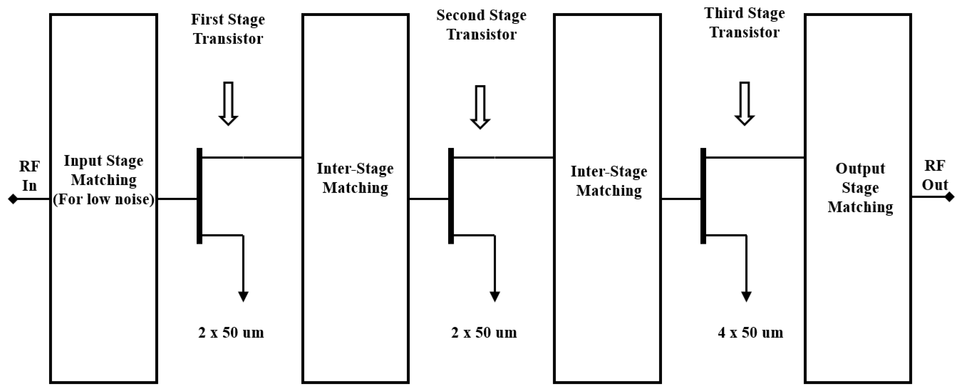
5.1. X-Band LNA Design Procedure

The X-Band LNA design covers a frequency range of 8 GHz to 12 GHz in the electromagnetic spectrum. A three-stage LNA was implemented using the 0.15   μ m low noise InGaAs pHEMT process. The small-signal parameters were extracted under a bias condition of
V g s = 0.3   V , V d s = 2   V .
This bias point was chosen to minimise current dissipation while providing the desired trade-off between gain and noise figure. Each stage was biased to maintain current uniformity across the amplifier. The design centre frequency was
f d = 10 GHz .
Figure 7 depicts the three-stage LNA structure for the X-band. Each transistor stage has distinct gate and drain lines for proper inter-stage matching and to ensure overall stability. Inductive source degeneration (feedback) is used in the first stage to bring the optimum noise match Γ opt closer to the gain match point, which helps in achieving a lower noise figure.

5.1.1. Stage-by-Stage Design Considerations

  • Stage one: The first stage consists of a transistor of size 2 × 75 μ m , using inductive source feedback for stabilisation. This feedback helps bring the optimum noise match Γ opt close to the gain match, thereby reducing the overall noise figure. The input source impedance is 50 Ω , and the input matching network was implemented using an LC combination (series inductor and capacitor).
  • Stage two: The second stage also employs a transistor of size 2 × 75 μ m . An inter-stage matching network is used between stages one and two to transform the output impedance of stage one to the input impedance of stage two. The goal is to provide the maximum stable gain and linearity while maintaining stability.
  • Stage three: The final stage uses a transistor of size 2 × 100 μ m . The output of stage two is matched to the input of stage three to maximise the overall gain. A parallel feedback network is introduced in this stage to achieve gain flatness and to boost output power handling.
Figure 8 shows the full schematic of the three-stage X-band LNA.
From Figure 8, the following key observations can be made:
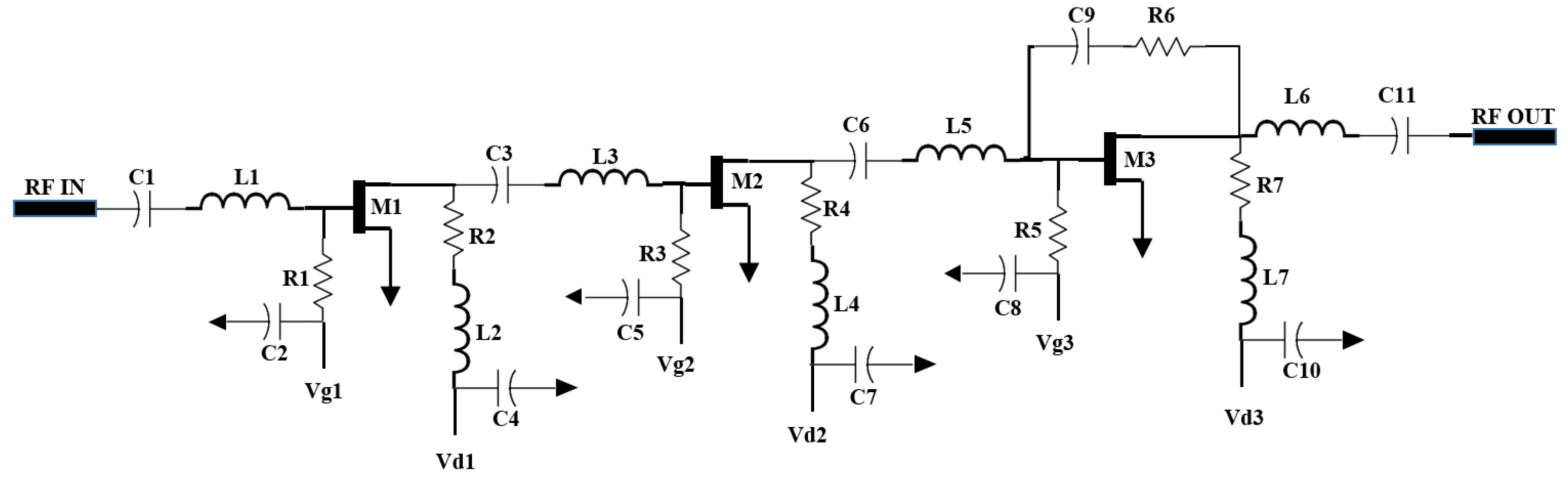
  • Capacitors C1 and C10 act as DC blocks, preventing DC voltage from flowing along the RF path.
  • Capacitors C2, C4, C5, C7, C8, and C9 are bypass or decoupling capacitors connected to the bias lines to reduce the coupling of RF signals into the power supply.
  • Resistors R1, R3, and R5 are high-value resistors used to isolate RF signals from the DC supply.
  • The input matching network for the first stage is formed by C1 and L1, ensuring that the amplifier sees Γ opt at the transistor’s gate when terminated in 50 Ω .
  • The output matching network is composed of L6 and C10, allowing for proper load matching.

5.1.2. Noise Figure Design Considerations

In designing LNAs, the noise factor (F) or noise figure (NF) is of paramount importance. For a transistor, the noise factor can be modelled by:
F ( Γ S ) = F min + R n Γ S Γ opt 2 ,
where F min is the minimum noise factor achievable by the device, Γ S is the source reflection coefficient, R n is the equivalent noise resistance, and Γ opt is the reflection coefficient at which F min occurs. By employing inductive source degeneration in the first stage and carefully designing the matching networks, the LNA is able to achieve a noise figure close to F min .

5.1.3. X-Band LNA S-Parameter Analysis

The S-parameters of the LNA are shown in Figure 9. The output and input return losses exceed 10 dB over the full frequency spectrum. The gain (Figure 10) was 40 dB with a 1 dB ripple over the designated range, while the lowest noise (Figure 11) at the resonance frequency of 10 GHz was 0.9 dB.

5.1.4. State-of-the-Art in X-Band LNA Design

Table 1 provides a comparison of state-of-the-art LNAs operating in the target X-band frequency range. These designs vary in process technology, application, frequency band, gain, noise figure, and power dissipation. The proposed design in [15] leverages the 0.15   μ m InGaAs pHEMT process to achieve a combination of high gain ( 40 dB) and low noise figure ( 0.9 dB).

5.2. K/Ka-Band LNA Design Procedure

The K/Ka-Band LNA covers the frequency range 23 GHz to 28 GHz, including the 24.25 GHz to 27.5 GHz band allocated for 5G applications [18]. Similar to the X-band LNA, this K/Ka-Band LNA is also a three-stage cascade design (see Figure 12) using a 0.15   μ m InGaAs pHEMT process. The design aims for both low noise figure and high gain while maintaining stability and adequate output power.

5.2.1. Stage-by-Stage Design Considerations

  • Stage one: The first stage uses a 2 × 50 μ m pHEMT with inductive source feedback to achieve the optimum noise match ( Γ opt ) for the target frequency. The inter-stage matching network transforms the 50 Ω input source impedance to the required noise match impedance.
  • Stage two: The second stage also uses a 2 × 50 μ m pHEMT. The inter-stage matching network ensures that the output impedance of stage one is properly matched to the input impedance of stage two to maintain maximum stable gain.
  • Stage three: A 4 × 50 μ m pHEMT is employed in the final stage to provide higher output power. Parallel feedback is introduced to enhance gain flatness across the entire band of operation.
Figure 13 shows the complete schematic of the three-stage K/Ka-Band LNA. Key aspects include:
  • C1 and C11 serve as DC blocking capacitors, preventing DC currents from flowing along the RF path.
  • C2, C4, C5, C7, C8, and C10 are power supply decoupling capacitors to isolate RF signals from the bias lines.
  • R1, R3, and R5 are large-valued resistors that help in reducing RF coupling into the DC supply.
  • The third stage employs a series RC feedback network (C9 and R6) to achieve the desired gain flatness.
  • M1, M2, and M3 denote the pHEMT devices in stages one, two, and three, respectively.

5.2.2. K/Ka-Band LNA S-Parameter Analysis

The LNA S-parameters are shown in Figure 14. It can be observed that the output and input return losses are greater than 10 dB for the entire band. The gain (Figure 15) was 30 dB with a ripple of 1 dB across the required band while the minimum noise (Figure 16) at the resonant frequency of 25 GHz was 1.5 dB.

5.2.3. Comparison with State-of-the-art K/Ka-Band LNAs

Table 2 lists state-of-the-art LNAs that operate in the K/Ka frequency band. Processes vary from CMOS, SiGe, GaAs to InP, designed for SATCOM or emerging 5G applications. Each design is characterised by its operating frequency, gain, noise figure, and power consumption. The design in [18] targets both 5G and SATCOM applications in the 23 GHz to 28 GHz band using a 0.15   μ m InGaAs pHEMT technology.

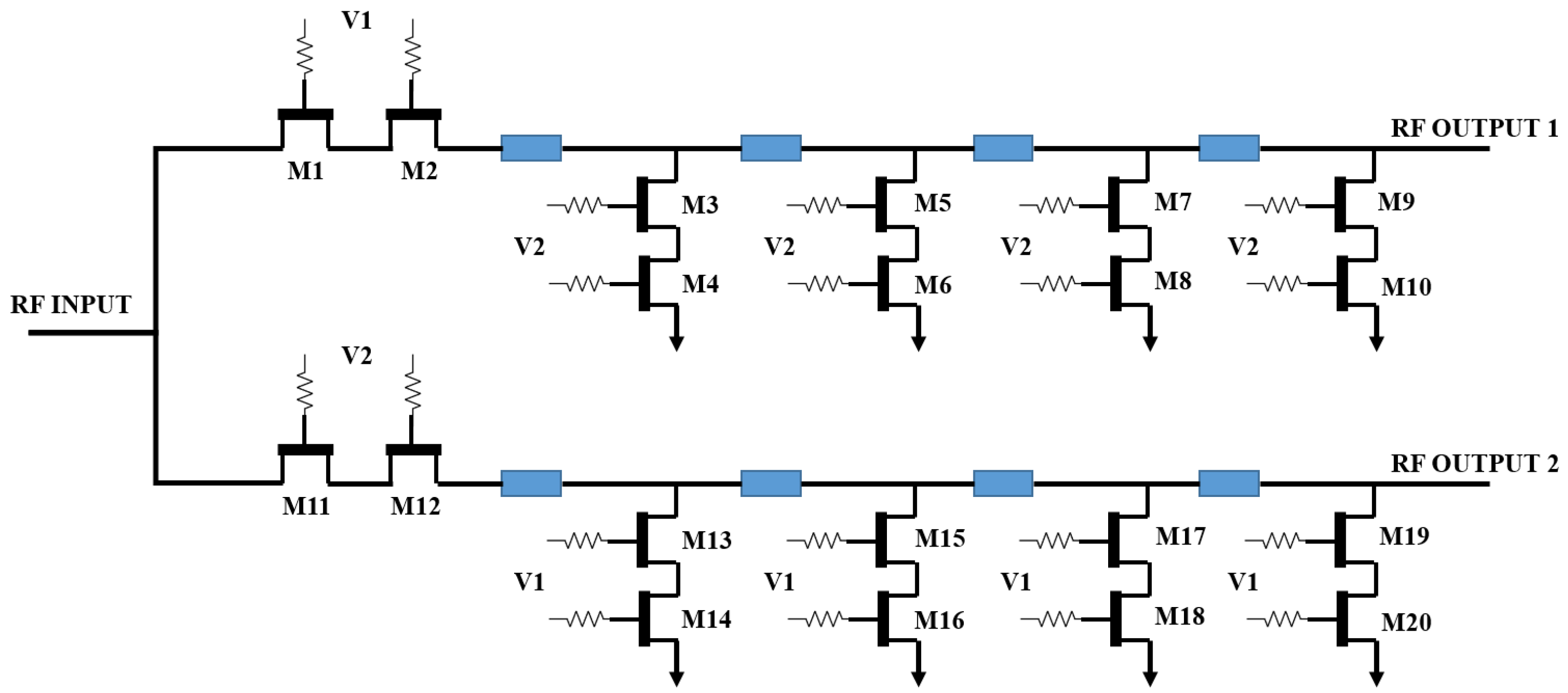
6. HARRF SPDT Design

The growing need for broadband RF switches stems from the ever-increasing demand for bandwidth and data rates in microwave and millimeter-wave transceiver systems [36,37]. These RF switches are pivotal components in a variety of wireless applications (including space-based systems) for controlling RF signal flow at both the input and output ports [17,38,39,40,41]. In wireless communication systems, RF switches must exhibit low insertion loss, high isolation, and a broad operating bandwidth extending up to millimeter-wave frequencies [18,42,43].
For millimeter-wave applications, FET-based switches are preferred over PIN diodes due to their ease of integration with other transceiver components, rapid switching speed, and low power dissipation [38,42]. However, the challenges with FET switches include reduced isolation at high frequencies, lower breakdown voltage, and limited power handling capabilities. These drawbacks are often attributed to the gate-drain parasitic capacitance, denoted as C g d . In this design, a 0.15   μ m pHEMT process from WIN Semiconductors Corporation is selected to realise a broadband Single-Pole Double-Throw (SPDT) switch suitable for satellite and 5G communication applications. Each branch of this well-matched SPDT switch is composed of four stacked FET units in shunt configuration, along with two series FETs to achieve higher voltage handling [44,45,46]. The presence of series FETs allows the SPDT switch to operate down to DC by isolating the off-state capacitance effectively.

6.1. FET Device Biasing

When used in switch applications, pHEMT devices are generally operated around 0 V DC bias. The gate control voltage for the “ON” state is 0 V, and for the “OFF” state it is driven below the pinch-off value (i.e., V g < V p ). In this work, the pinch-off voltage V p is approximately −1.5 V. Thus:
  • ON State: Gate voltage V g = 0   V . The low gate-source voltage produces a low channel resistance ( R on ) and enables the RF signal to pass from drain to source.
  • OFF State: Gate voltage V g = 1.5   V . The transistor channel is pinched off, creating a high channel resistance ( R off ), thereby blocking the RF signal path.
Since the RF signal traverses from drain to source, the gate serves as the control terminal. Large-value resistors are typically employed in the gate bias network to isolate RF signals from the DC supply lines.
Figure 17 illustrates typical I-V characteristics of a depletion-mode FET at various negative gate-source bias levels near the 0 V operating point. As V g s decreases below pinch-off, the drain current I d significantly drops, corresponding to the “OFF” state.
Designing an SPDT switch for high-frequency operation (from DC up to 50 GHz) requires a thorough understanding of scattering parameters (S-parameters). S-parameters quantitatively describe how incident waves at each port of a multiport network are transmitted or reflected.

6.2. Scattering Parameters (S-Parameters)

Scattering parameters (S-parameters) characterise how RF signals are transmitted and reflected between ports in a multi-port network. For a three-port device such as a single-pole double-throw (SPDT) switch, the S-parameter matrix, denoted by the 3 × 3 matrix S , is given by
S = S 11 S 12 S 13 S 21 S 22 S 23 S 31 S 32 S 33 ,
where each element S i j represents the ratio of the reflected wave at port i to the incident wave at port j.
  • S 11 is the reflection coefficient at port 1.
  • S 21 , S 31 are the transmission coefficients from port 1 to ports 2 and 3, respectively.
  • S 12 , S 13 represent the transmission from ports 2 and 3 back to port 1, respectively.
  • S 22 is the reflection coefficient at port 2.
  • S 33 is the reflection coefficient at port 3.
  • S 23 , S 32 indicate the transmission between ports 2 and 3.

6.2.1. Network Power Relations

For an N-port passive network, the scattered (reflected) signals must not exceed the incident signals in terms of total power. In the three-port case ( N = 3 ) , one of the passivity constraints can be expressed as
m = 1 3 S n m 2 1 , for each n = 1 , 2 , 3 .
when the network is lossless and reciprocal, the S-parameter matrix is unitary and symmetric. Unitarity implies that
S H S = I ,
where S H is the Hermitian (conjugate transpose) of S , and I is the 3 × 3 identity matrix.
Because each S-parameter element S i j is, in general, a complex-valued function of frequency ω (or equivalently f), we have:
S i j = S i j ( ω ) = | S i j ( ω ) | e j ϕ i j ( ω ) ,
where ϕ i j ( ω ) denotes the phase response. Examining how S i j varies with ω is crucial for designing wideband or multi-band circuits such as SPDT switches in reconfigurable front-ends.
A useful measure is the derivative of the phase with respect to ω , often related to the group delay τ g :
τ g ( ω ) = d d ω S i j ( ω ) .
Minimising large variations in group delay is beneficial for signal integrity.

6.2.2. Integral Measures over Frequency

In many wideband applications, one may be interested in the integrated performance of a scattering parameter over a specified bandwidth Δ f . For example, the average transmitted power coefficient T ¯ i j from port j to port i over a bandwidth Δ f = f 2 f 1 can be expressed as
T ¯ i j = 1 Δ f f 1 f 2 S i j ( f ) 2 d f .
Such integral measures provide insight into the average behaviour of the SPDT switch or other multi-port networks across the band of interest.

6.3. Incident and Reflected Waves

Let a i denote the incident wave at port i, and b i denote the reflected (or scattered) wave at port i. In vector form, the relationships among these waves can be written as
b 1 b 2 b 3 = S 11 S 12 S 13 S 21 S 22 S 23 S 31 S 32 S 33 a 1 a 2 a 3 .
Expanding (47) in terms of its elements yields:
b i = j = 1 3 S i j a j , i { 1 , 2 , 3 } .

Power Consistency Check

The incident power P in at port j can be related to | a j | 2 , and the reflected power P ref at port i can be related to | b i | 2 . For a single excitation scenario (where all incident waves except a j are zero), it follows from (48) that
b i = S i j a j .
Thus, the ratio of reflected power at port i to the incident power at port j is
P ref , i P in , j = | b i | 2 | a j | 2 = S i j 2 .
If the SPDT switch (or multi-port network) is passive, the sum of reflected powers across all ports must not exceed the total incident power. Hence, if a j 0 and a k = 0 for k j :
i = 1 3 | b i | 2 = i = 1 3 S i j 2 | a j | 2 | a j | 2 ,
which is consistent with the passivity constraint in (42).
These theoretical considerations guide the design and optimisation of SPDT switches used in reconfigurable radio front-ends, ensuring minimal loss, high isolation, and robust performance across the targeted frequency range.

6.4. Key Performance Metrics

6.4.1. Insertion Loss

Insertion loss quantifies the signal power attenuation when the switch is in the “ON” state (or through-path). In dB form:
L ins ( f ) = 10 log 10 P input P output
Equivalently, if S 21 (or S 31 ) is the transmission parameter from input to the active output port, the insertion loss (in dB) can also be expressed as:
L ins ( f ) = 20 log 10 S 21 .

6.4.2. Isolation

Isolation refers to how well the switch suppresses signals leaking into the “OFF” port. If P leak is the power reaching the isolated port and P input is the input power, the isolation I in dB is:
I ( f ) = 10 log 10 P leak P input .
Often, in terms of S-parameters, the isolation to the “OFF” port from the input port is given by:
Isolation ( dB ) = 20 log 10 S 31 ( when port 3 is OFF ) .

6.4.3. Return Loss

Return loss measures how much of the signal reflects back to the source, typically due to impedance mismatches. It is defined by:
R L ( f ) = 20 log 10 Γ , Γ = Z in Z 0 Z in + Z 0 ,
where Z in is the input impedance at the reference plane and Z 0 is the characteristic impedance (commonly 50   Ω ).
A distributed topology is employed for the SPDT switch to achieve broadband performance, as depicted in Figure 18. Specifically, the design combines:
  • Two series FETs to improve power handling and ensure operation down to DC.
  • Four shunt-stacked FET units to enhance isolation by absorbing the off-state capacitance into a low-pass filter section.
One challenge in designing such a reconfigurable network with an SPDT switch is to maintain optimal impedance matching in both switch states (“ON” and “OFF”) to minimize insertion loss. Large resistors (>k ω ) are used at the source and drain terminals (labelled as V1 and V2 in Figure 18) for biasing, thereby minimising additional loss in the RF path. The drain voltages for the series FETs alternate between 0 V and 2 V, depending on whether a particular arm is in the “ON” or “OFF” state (see Table 3).
When the left arm is active (ON), the series FETs on that arm are biased at V g = 0 V (low R on ), while the shunt FETs in that arm are pinched off (high R off ). Meanwhile, the right arm remains in the OFF state, with its series FETs biased at V g = 1.5 V , thereby achieving high isolation. The gate control voltages V1 and V2 act in a complementary fashion: when V1 is low, V2 is high, and vice versa. This arrangement ensures that at any time only one path is active (ON) while the other path is isolated (OFF).

6.5. Series vs. Shunt FET Configuration

  • Series FETs: Used primarily to handle higher power and to lower the ON resistance. By stacking multiple FETs in series, the drain-source voltage across each FET is reduced, mitigating breakdown issues at high power levels or high operating voltages.
  • Shunt FETs: These help improve isolation by providing an alternate low-impedance path to ground when they are turned ON (pinched-off for the main path). In the distributed design, the parasitic off-state capacitance of the shunt FETs can be absorbed into the matching network, effectively extending the bandwidth of operation.
In this design, each series FET is sized at 3 × 275 μ m to provide the necessary current handling capability. Table 4 shows some key design requirements and corresponding simulated performance at three spot frequencies (10 GHz, 26 GHz, and 38 GHz).
From Table 4, it can be seen that the design meets or exceeds the typical requirements for reflection coefficients ( S 11 and S 22 ) and isolation ( S 12 ) across a wide frequency range. The insertion loss ( | S 21 | ) is also held to approximately 3 dB or less, which is acceptable for many wideband radar, 5G, and SATCOM front-end applications.

7. Result Analysis of Wideband SPDT Switch and Reconfigurable Front-End

Figure 19 shows the insertion loss, input, and output return loss of the designed SPDT switch, while Figure 20 illustrates the isolation performance. From Figure 19, the return loss ( S 11 , S 22 ) remains better than 10 dB over the design bandwidth, and the isolation between the ON and OFF ports ranges from 40 to 75 dB, as shown in Figure 20.
The considerable insertion loss in the wideband SPDT switch is due to several reasons, including resistive losses in the switching transistors, parasitic capacitances, impedance mismatches, and substrate losses. At elevated frequencies (exceeding 60 GHz), S 21 (transmission coefficient) markedly declines, attaining −12 dB at 90 GHz, signifying substantial power attenuation. Resistive losses from the on-state resistance ( R o n ) elevate insertion loss, whilst parasitic capacitances ( C d s , C g d ) cause frequency-dependent attenuation, hence diminishing transmission efficiency as capacitance-related reactance decreases with rising frequency. Mismatch losses are apparent in the elevated S 11 and S 22 values, resulting in signal reflections and decreased power transfer efficiency, while dielectric and substrate losses further impair performance at millimetre-wave frequencies. The cumulative insertion loss can be quantitatively represented as the total of resistive, capacitive, and mismatch-induced losses, with high-frequency signal attenuation intensified by substrate dielectric loss. To alleviate these losses, it is advisable to implement design optimisations, including the reduction of R o n through shorter gate-length FETs, the minimisation of parasitic capacitances using enhanced layout approaches, the improvement of impedance matching through multi-stage networks, and the use of low-loss dielectric substrates. Employing these strategies can markedly enhance the switch’s performance for millimetre-wave and 5G applications, guaranteeing improved signal integrity and reduced insertion loss over the operating frequency spectrum.
Table 4 (shown earlier) summarises the design requirements and performance at spot frequencies of 10 GHz, 26 GHz, and 38 GHz. The proposed switch meets or exceeds these requirements, thereby satisfying minimum industry standards.

7.1. Comparison with State-of-the-Art Designs

Table 5 highlights the performance of the proposed SPDT switch relative to other published designs at 10 GHz. Although some references report narrower bandwidths, the proposed design features substantially higher isolation ( 70 dB) while maintaining acceptable return loss. This is advantageous for wideband receiver front-ends where high isolation is crucial for signal integrity.
As shown in Table 5, the proposed SPDT switch significantly improves isolation relative to references [47,48,49,50], while retaining an acceptable insertion loss. Moreover, many prior works focus on narrower bandwidths, whereas the presented design has a wideband capability, covering from DC up to about 50 GHz.

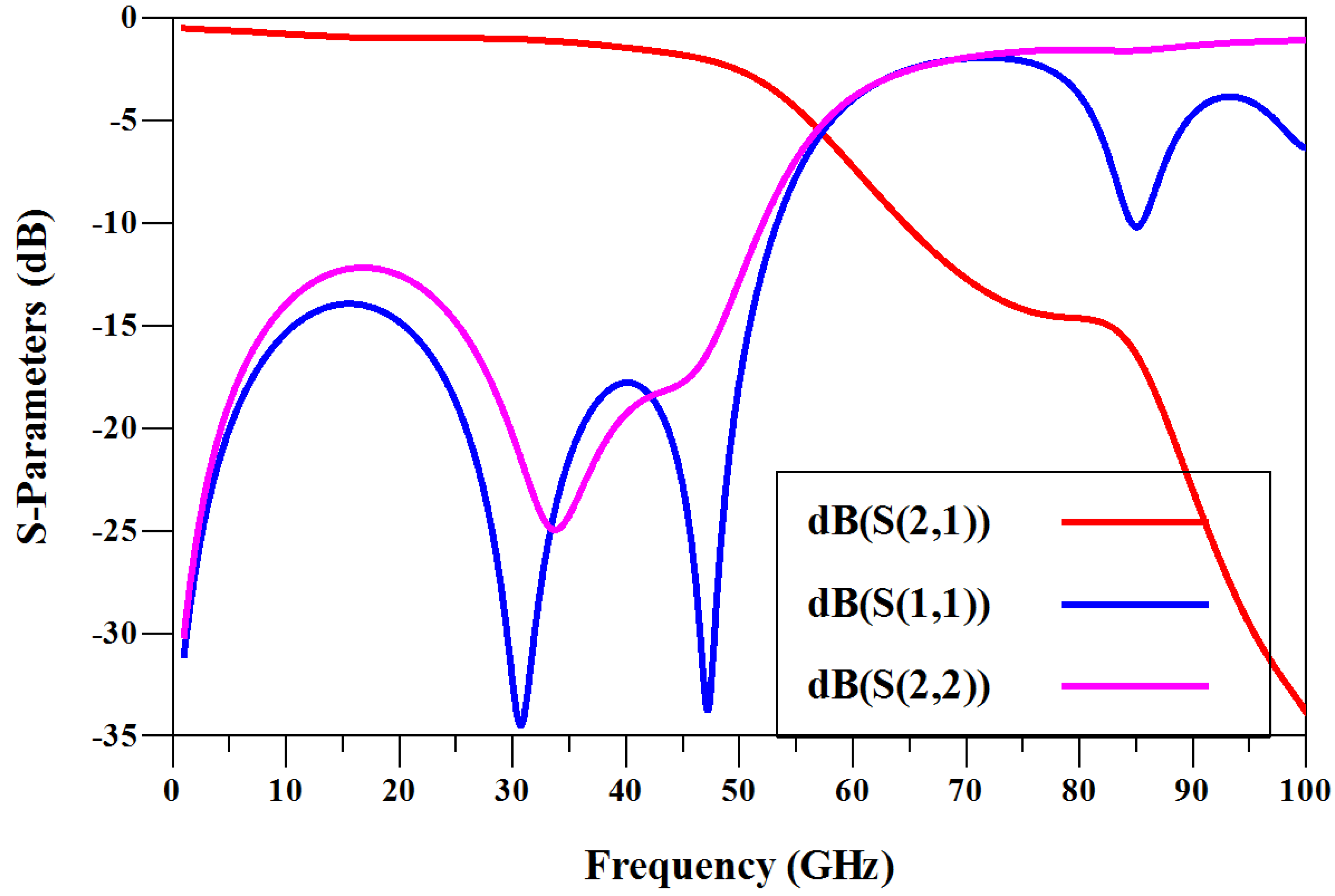
7.2. SPDT Integration with X-Band ON and K/Ka-Band OFF

In a switchable wideband receiver front-end configuration, only one band is active while the other is pinched off (OFF). In this section, the X-band LNA path is switched ON, and the K/Ka-band path is switched OFF.

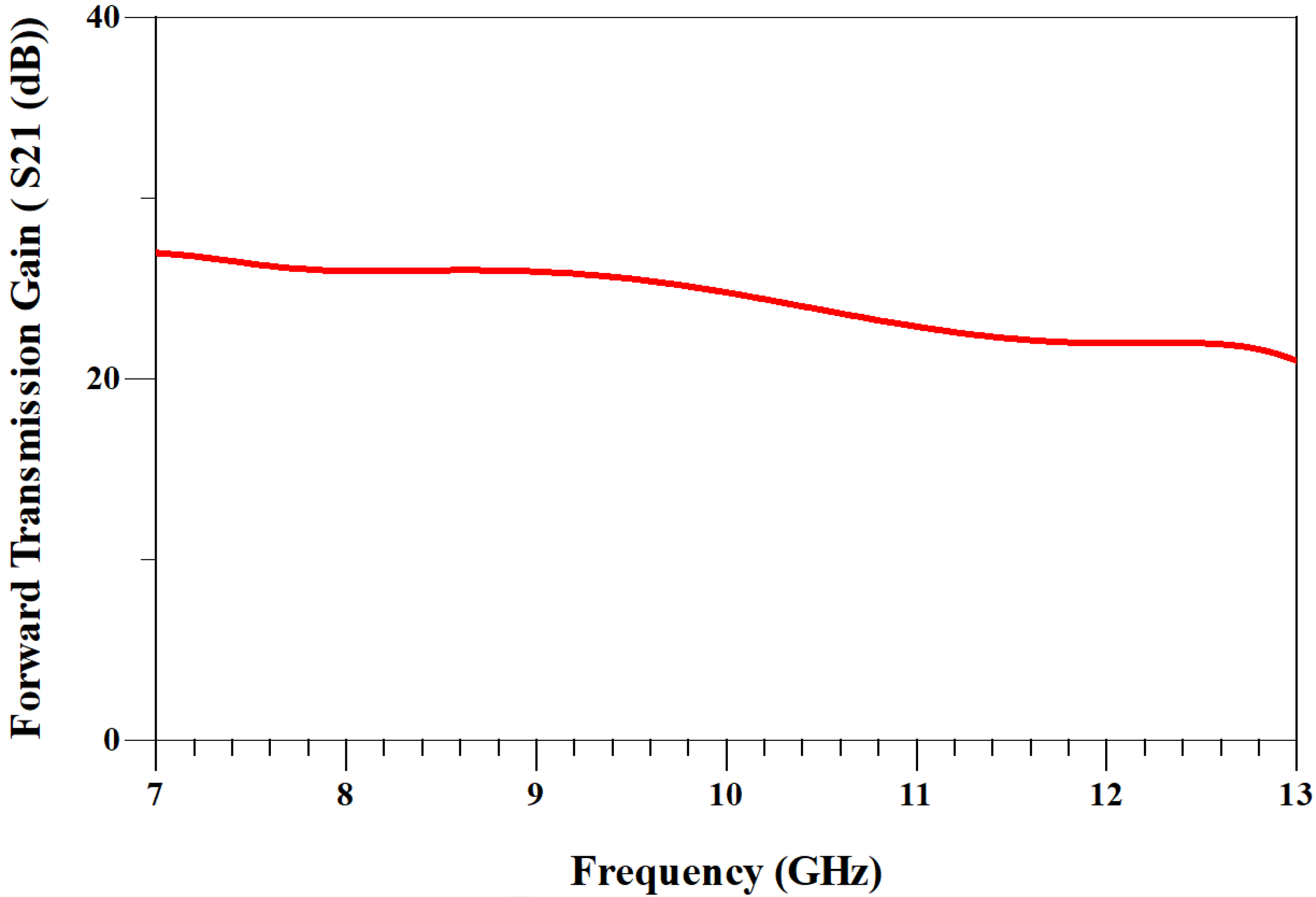
7.2.1. Gain Performance

Figure 21 shows the simulated gain for the receiver front-end with the X-band arm ON over 8–12 GHz. The simulated gain ranges from 23 dB to 27 dB at room temperature, demonstrating robust performance in the X-band.

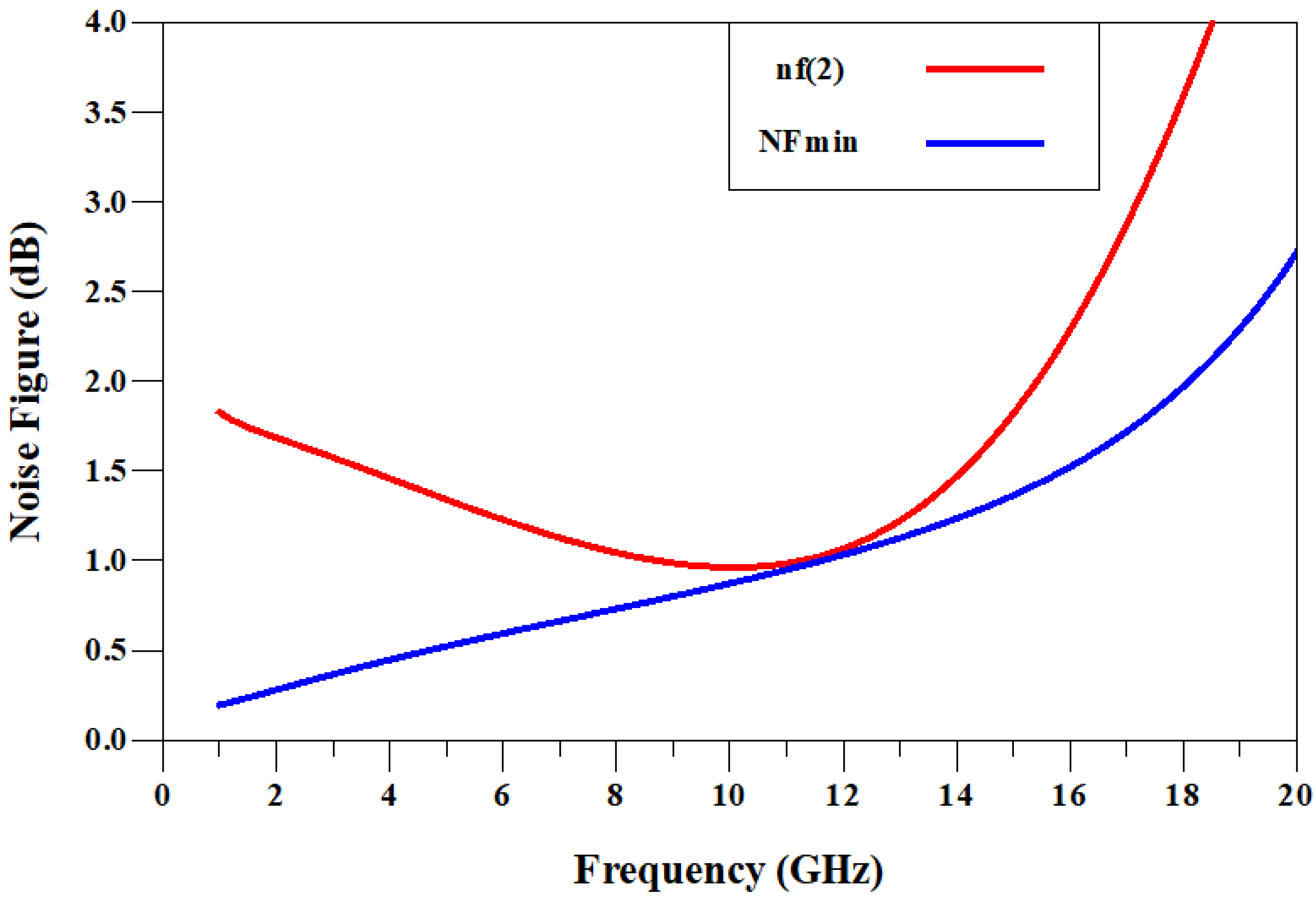
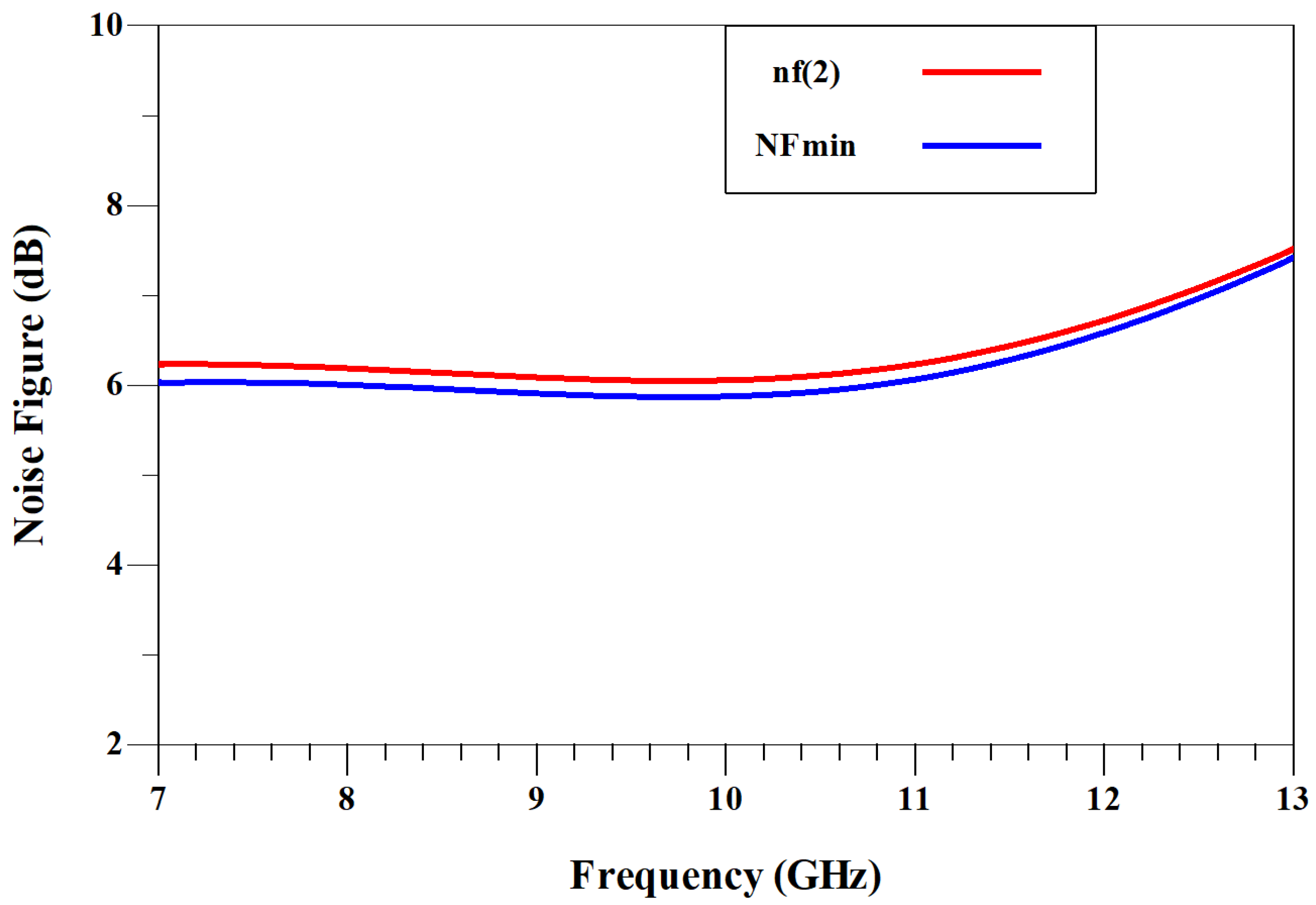
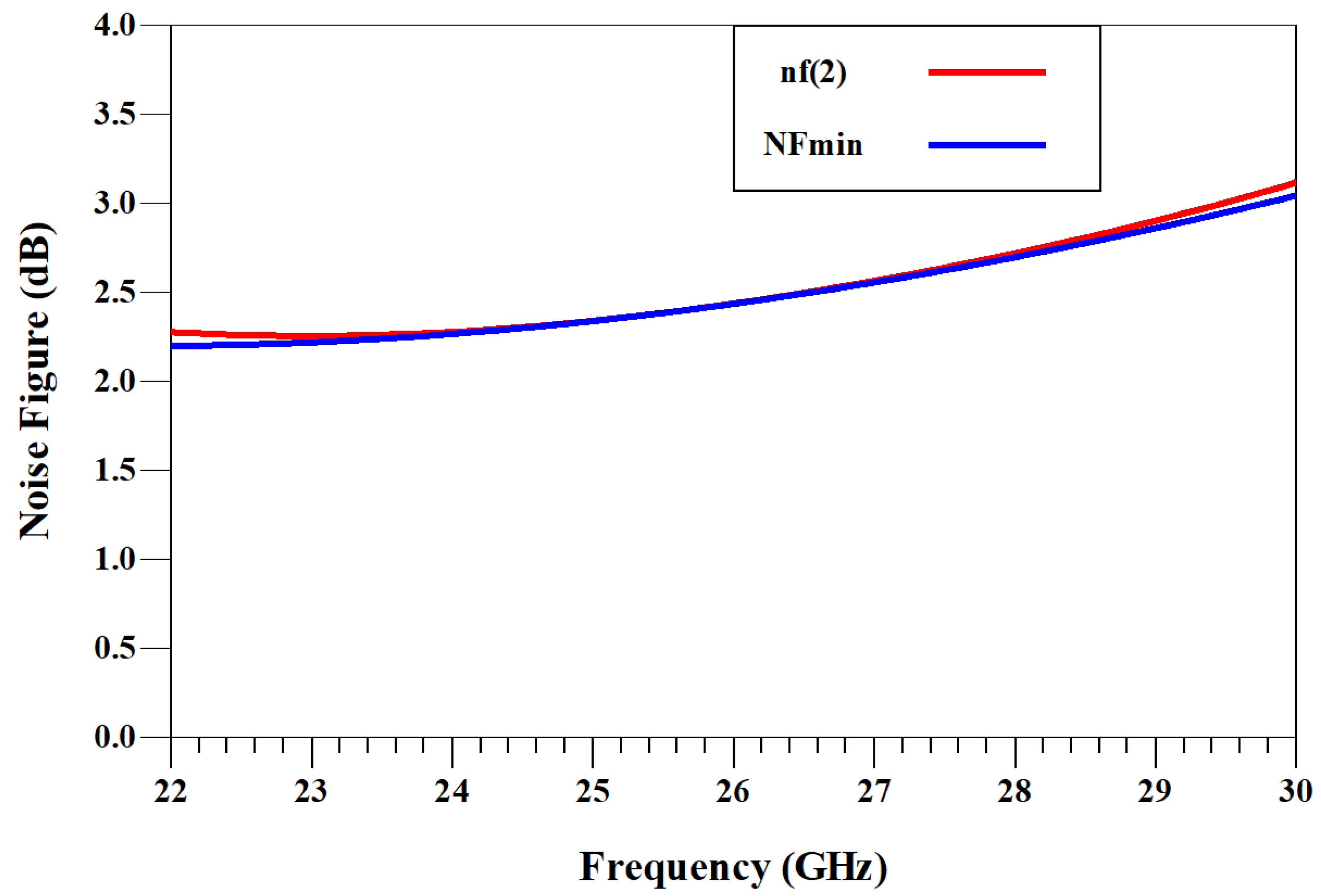
7.2.2. Noise Performance

Figure 22 illustrates the noise figure (NF) of the receiver front-end with the K/Ka-band arm turned off. The X-band arm’s noise figure remains below 10 dB over the frequency range of interest (8–12 GHz). Since the K/Ka-band path is off, its contribution to NF and gain in this mode is negligible.

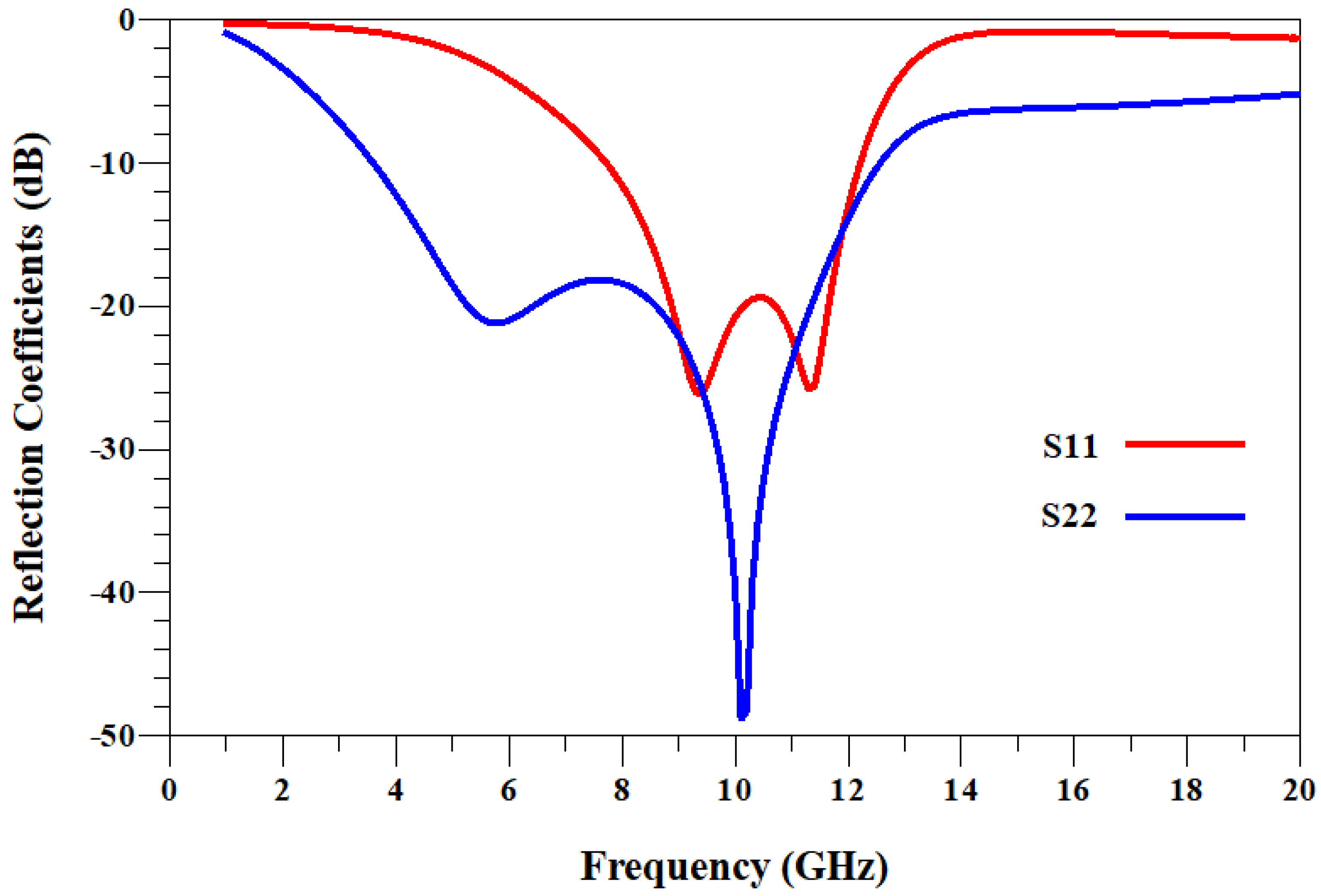
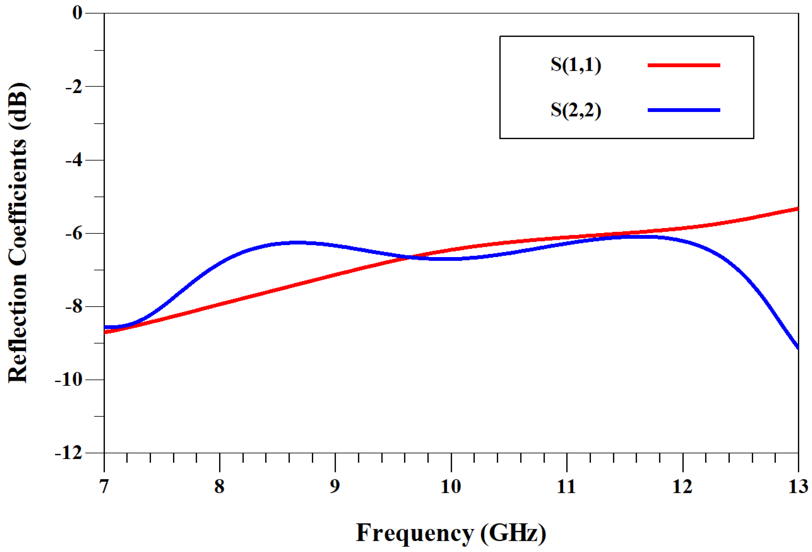
7.2.3. Reflection Coefficients

Figure 23 shows the input and output reflection coefficients for the active X-band arm. Both reflection coefficients are better than 5 dB across 8–12 GHz, which is acceptable for many practical applications.

7.2.4. Stability

The stability factor (based on Rollet’s criterion) is shown in Figure 24, where the design remains unconditionally stable across all frequencies of interest. This indicates that no risk of oscillation arises under typical source and load impedances.

7.3. SPDT Integration with X-Band OFF and K/Ka-Band ON

Next, the K/Ka-band path is enabled (ON) while the X-band path is disabled (OFF). The following subsections summarise the resulting simulations over 23–28 GHz.

7.3.1. Gain Performance

Figure 25 presents the simulated gain between 23 dB and 27 dB for the K/Ka-band arm from 23 to 28 GHz.

7.3.2. Noise Performance

Figure 26 shows the K/Ka-band noise figure, which varies from 2.3 dB to 2.6 dB. By turning the X-band path off, the circuit ensures minimal interference or additional noise contribution in the K/Ka-band.

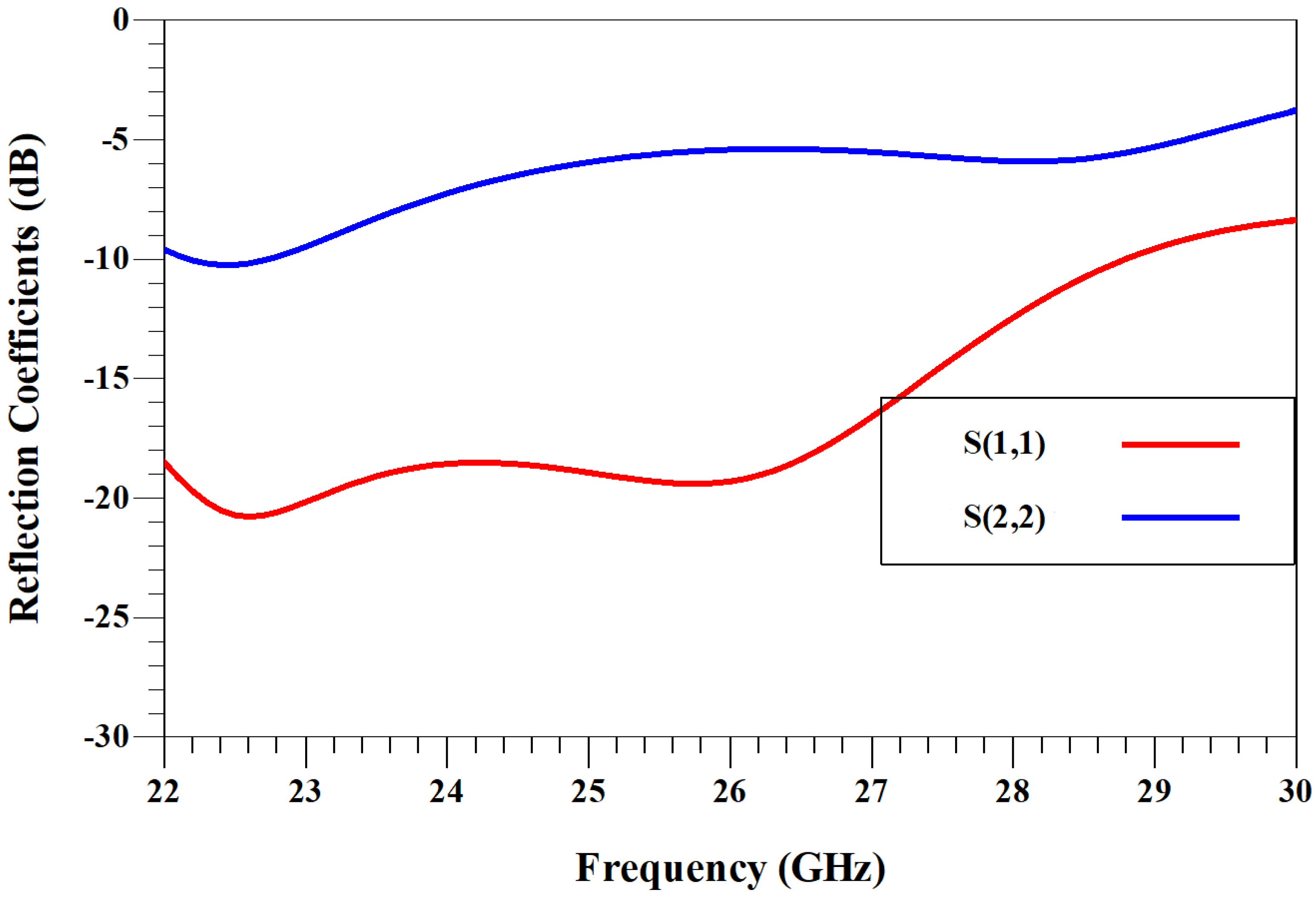
7.3.3. Reflection Coefficients
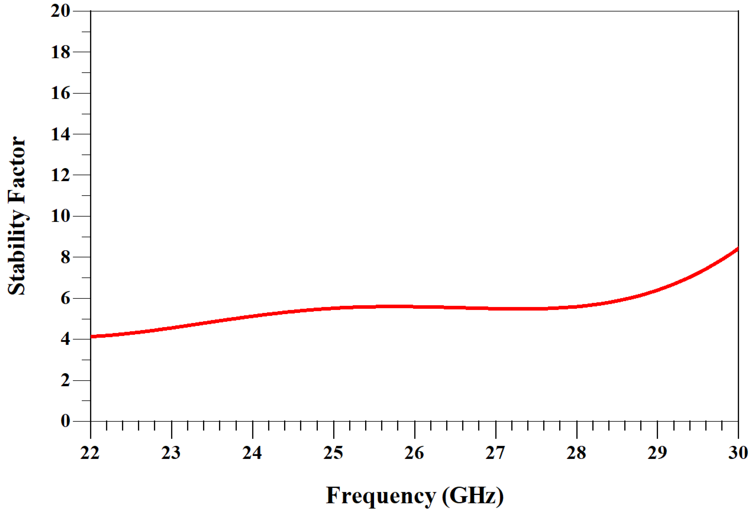
In Figure 27, the input and output reflection coefficients remain better than 5 dB throughout 23–28 GHz. This indicates a suitably matched design for the K/Ka-band.

7.3.4. Stability

Figure 28 illustrates the unconditional stability of the design for the entire 23–28 GHz band. This ensures reliable operation in satellite and 5G applications where large signal variations and different load conditions can occur.

8. Conclusions

A highly adaptive reconfigurable receiver front-end (HARRF) has been presented for multi-band operation covering X-band (8–12 GHz) and K/Ka-band (23–28 GHz), integrating two three-stage LNAs and a Single-Pole Double-Throw (SPDT) switch in a 0.15   μ m InGaAs pHEMT process. The X-band LNA achieves 23–27 dB of gain, maintains a noise figure (NF) of approximately 1.7–2.0 dB, and retains input/output return losses better than 5 dB with unconditional stability ( K > 1 ). The K/Ka-band LNA exhibits a gain of 23–27 dB and an NF of 2.3–2.6 dB while preserving stability over its band. The SPDT switch demonstrates low insertion loss (∼3 dB) up to 50 GHz, isolation levels of 40–75 dB, and | S 11 | , | S 22 |   10 dB , ensuring minimal interference between X-band and K/Ka-band paths. Together, these components enable efficient frequency switching, high gain, and low noise over wide bands, reducing form factor and cost and making this solution viable for next-generation radar, satellite, and 5G mmWave transceivers.

Author Contributions

Conceptualization, M.U. and S.E. (Sunday Ekpo); methodology, M.U.; software, M.U. and F.E.; validation, M.U., S.E. (Sunday Ekpo), S.E. (Sunday Enahoro), R.U., Y.A.-Y. and F.E.; formal analysis, M.U.; investigation, M.U.; resources, M.U. and S.E. (Sunday Ekpo); data curation, M.U.; writing—original draft preparation, M.U.; writing—review and editing, M.U., S.E. (Sunday Ekpo), S.E. (Sunday Enahoro), R.U., Y.A.-Y. and F.E.; supervision, S.E. (Sunday Ekpo); project administration, S.E. (Sunday Ekpo). All authors have read and agreed to the published version of the manuscript.

Funding

This research received no external funding.

Data Availability Statement

Data are contained within the article.

Conflicts of Interest

The authors declare no conflicts of interest.

References

  1. Paul, U.; Liu, J.; Troia, S.; Falowo, O.; Maier, G. Traffic-profile and machine learning based regional data center design and operation for 5G network. J. Commun. Netw. 2019, 21, 569–583. [Google Scholar]
  2. Uko, M.; Ekpo, S.; Elias, F.; Alabi, S. A 3.2–3.8 GHz low-noise amplifier for 5G/6G satellite-cellular convergence applications. e-Prime-Adv. Electr. Eng. Electron. Energy 2024, 8, 100559. [Google Scholar] [CrossRef]
  3. Uko, M.; Ekpo, S.C.; Enahoro, S.; Elias, F. Performance Optimization of 5G–Satellite Integrated Networks for IoT Applications in Smart Cities: A Two-Ray Propagation Model Approach. Smart Cities 2024, 7, 3895–3913. [Google Scholar] [CrossRef]
  4. Cisco. Cisco Annual Internet Report—Cisco Annual Internet Report (2018–2023) White Paper. 2022. Available online: https://www.cisco.com/c/en/us/solutions/collateral/executive-perspectives/annual-internet-report/white-paper-c11-741490.html (accessed on 14 March 2025).
  5. Bhagavatula, V. Exploring Multimode Cellular Transceiver Design: A Short Tutorial. IEEE Solid-State Circuits Mag. 2021, 13, 35–47. [Google Scholar] [CrossRef]
  6. Seth, S.; Kwon, D.H.; Venugopalan, S.; Son, S.W.; Zuo, Y.; Bhagavatula, V.; Lim, J.; Oh, D.; Cho, T.B. A Dynamically Biased Multiband 2G/3G/4G Cellular Transmitter in 28 nm CMOS. IEEE J. Solid-State Circuits 2016, 51, 1096–1108. [Google Scholar] [CrossRef]
  7. Hosseinian, M.; Choi, J.P.; Chang, S.H.; Lee, J. Review of 5G NTN standards development and technical challenges for satellite integration with the 5G network. IEEE Aerosp. Electron. Syst. Mag. 2021, 36, 22–31. [Google Scholar]
  8. Völk, F.; Schlichter, T.; Kaltenberger, F.; Heyn, T.; Casati, G.; Schwarz, R.T.; Knopp, A. Field trial of a 5G non-terrestrial network using OpenAirInterface. IEEE Open J. Veh. Technol. 2022, 3, 243–250. [Google Scholar] [CrossRef]
  9. Pastukh, A.; Tikhvinskiy, V.; Dymkova, S.; Varlamov, O. Challenges of Using the L-Band and S-Band for Direct-to-Cellular Satellite 5G-6G NTN Systems. Technologies 2023, 11, 110. [Google Scholar] [CrossRef]
  10. Manco, J.; Dayoub, I.; Nafkha, A.; Alibakhshikenari, M.; Thameur, H.B. Spectrum sensing using software defined radio for cognitive radio networks: A survey. IEEE Access 2022, 10, 131887–131908. [Google Scholar]
  11. Tuninato, R.; Garello, R. 5G NTN Primary Synchronization Signal: An Improved Detector for Handheld Devices. IEEE Open J. Commun. Soc. 2024, 5, 3792–3803. [Google Scholar]
  12. Rappaport, T.S.; Xing, Y.; MacCartney, G.R.; Molisch, A.F.; Mellios, E.; Zhang, J. Overview of Millimeter Wave Communications for Fifth-Generation (5G) Wireless Networks—With a Focus on Propagation Models. IEEE Trans. Antennas Propag. 2017, 65, 6213–6230. [Google Scholar] [CrossRef]
  13. LaRocca, T.R.; Thai, K.; Snyder, R.; Jai, R.; Kultran, D.; Fordham, O.; Wu, B.Y.C.; Yang, Y.; Watanabe, M.K.; Rodgers, P.; et al. Secure Satellite Communication Digital IF CMOS Q-Band Transmitter and K-Band Receiver. IEEE J. Solid-State Circuits 2019, 54, 1329–1338. [Google Scholar] [CrossRef]
  14. Boccardi, F.; Heath, R.W.; Lozano, A.; Marzetta, T.L.; Popovski, P. Five disruptive technology directions for 5G. IEEE Commun. Mag. 2014, 52, 74–80. [Google Scholar] [CrossRef]
  15. Uko, M.; Ekpo, S. 8–12 GHz pHEMT MMIC Low-Noise Amplifier for 5G and Fiber-Integrated Satellite Applications. Int. Rev. Aerosp. Eng. (IREASE) 2020, 13, 99. [Google Scholar] [CrossRef]
  16. Ekpo, S.; George, D. 4–8 GHz LNA design for a Highly Adaptive Small Satellite Transponder using InGaAs pHEMT Technology. In Proceedings of the 2010 IEEE 11th Annual Wireless and Microwave Technology Conference (WAMICON), Melbourne, FL, USA, 12–13 April 2010; pp. 1–4. [Google Scholar] [CrossRef]
  17. Ekpo, S.C.; George, D. Impact of Noise Figure on a Satellite Link Performance. IEEE Commun. Lett. 2011, 15, 977–979. [Google Scholar] [CrossRef]
  18. Uko, M.; Ekpo, S. A 23–28 GHz pHEMT MMIC Low-Noise Amplifier for Satellite-Cellular Convergence Applications. Int. Rev. Aerosp. Eng. J. 2021, 14, 1–10. [Google Scholar]
  19. Bhaumik, S.; Kettle, D. Broadband X-band low noise amplifier based on 70 nm GaAs metamorphic high electron mobility transistor technology for deep space and satellite communication networks and oscillation issues. IET Microw. Antennas Propag. 2010, 4, 1208–1215. [Google Scholar] [CrossRef]
  20. Nikbakhsh, M.R.; Abiri, E.; Ghasemian, H.; Salehi, M.R. Two-stage current-reused variable-gain low-noise amplifier for X-band receivers in 65 nm complementary metal oxide semiconductor technology. IET Circuits Devices Syst. 2018, 12, 630–637. [Google Scholar]
  21. Davulcu, M.; Çalişkan, C.; Kalyoncu, I.; Gurbuz, Y. An X-Band SiGe BiCMOS Triple-Cascode LNA With Boosted Gain and P1dB. IEEE Trans. Circuits Syst. II Exp. Briefs 2018, 65, 994–998. [Google Scholar] [CrossRef]
  22. Nam, H.; Nguyen, V.V.; Trinh, V.S.; Song, J.M.; Lee, B.H.; Park, J.D. A Full X-Band Phased-Array Transmit/Receive Module Chip in 65-nm CMOS Technology. IEEE Access 2020, 8, 76182–76192. [Google Scholar] [CrossRef]
  23. Çağlar, A.; Yelten, M.B. A 180-nm X-Band Cryogenic CMOS LNA. IEEE Microw. Wirel. Components Lett. 2020, 30, 395–398. [Google Scholar] [CrossRef]
  24. Abelan, B.A.; Seelmann-Eggebert, M.; Bruch, D.; Leuther, A.; Massler, H.; Baldischweiler, B.; Schlechtweg, M.; Gallego-Puyol, J.D.; Lopez-Fernandez, I.; Diez-Gonzalez, C.; et al. 4–12 and 25–34 GHz Cryogenic mHEMT MMIC Low-Noise Amplifiers. IEEE Trans. Microw. Theory Tech. 2012, 60, 4080–4088. [Google Scholar] [CrossRef]
  25. Cha, E.; Wadefalk, N.; Nilsson, P.; Schleeh, J.; Moschetti, G.; Pourkabirian, A.; Tuzi, S.; Grahn, J. 0.3–14 and 16–28 GHz Wide-Bandwidth Cryogenic MMIC Low-Noise Amplifiers. IEEE Trans. Microw. Theory Tech. 2018, 66, 4860–4869. [Google Scholar] [CrossRef]
  26. Tabarani, F.; Boccia, L.; Purtova, T.; Shamsafar, A.; Schumacher, H.; Amendola, G. 0.25-μm BiCMOS System-on-Chip for K-/Ka-Band Satellite Communication Transmit–Receive Active Phased Arrays. IEEE Trans. Microw. Theory Tech. 2018, 66, 2325–2339. [Google Scholar] [CrossRef]
  27. Pang, J.; Li, Z.; Kubozoe, R.; Luo, X.; Wu, R.; Wang, Y.; You, D.; Fadila, A.A.; Saengchan, R.; Nakamura, T.; et al. A 28-GHz CMOS Phased-Array Beamformer Utilizing Neutralized Bi-Directional Technique Supporting Dual-Polarized MIMO for 5G NR. IEEE J. Solid-State Circuits 2020, 55, 2371–2386. [Google Scholar] [CrossRef]
  28. Kim, H.T.; Park, B.S.; Song, S.S.; Moon, T.S.; Kim, S.H.; Kim, J.M.; Chang, J.Y.; Ho, Y.C. A 28-GHz CMOS Direct Conversion Transceiver With Packaged 2 × 4 Antenna Array for 5G Cellular System. IEEE J. Solid-State Circuits 2018, 53, 1245–1259. [Google Scholar] [CrossRef]
  29. Sadhu, B.; Tousi, Y.; Hallin, J.; Sahl, S.; Reynolds, S.K.; Renström, O.; Sjogren, K.; Haapalahti, O.; Mazor, N.; Bokinge, B.; et al. A 28-GHz 32-Element TRX Phased-Array IC With Concurrent Dual-Polarized Operation and Orthogonal Phase and Gain Control for 5G Communications. IEEE J. Solid-State Circuits 2017, 52, 3373–3391. [Google Scholar] [CrossRef]
  30. Wang, Y.; You, D.; Fu, X.; Nakamura, T.; Fadila, A.A.; Someya, T.; Kawaguchi, A.; Qiu, J.; Pang, J.; Yanagisawa, K.; et al. A Ka-Band SATCOM Transceiver in 65-nm CMOS With High-Linearity TX and Dual-Channel Wide-Dynamic-Range RX for Terrestrial Terminal. IEEE J. Solid-State Circuits 2022, 57, 356–370. [Google Scholar] [CrossRef]
  31. Uchida, H.; Takatsu, S.; Nakahara, K.; Katoh, T.; Itoh, Y.; Imai, R.; Yamamoto, M.; Kadowaki, N. Ka-band multistage MMIC low-noise amplifier using source inductors with different values for each stage. IEEE Microw. Guid. Wave Lett. 1999, 9, 71–72. [Google Scholar] [CrossRef]
  32. Ekpo, S.; Kharel, R.; Uko, M. A Broadband LNA Design in Common-Source Configuration for Reconfigurable Multi-standards Multi-bands Communications. In Proceedings of the 2018 ARMMS RF and Microwave Conference, Thame, UK, 23–24 April 2018; pp. 1–10. [Google Scholar]
  33. Nikandish, G.; Yousefi, A.; Kalantari, M. A Broadband Multistage LNA With Bandwidth and Linearity Enhancement. IEEE Microw. Wirel. Components Lett. 2016, 26, 834–836. [Google Scholar] [CrossRef]
  34. Ma, Q.; Leenaerts, D.M.W.; Baltus, P.G.M. Silicon-Based True-Time-Delay Phased-Array Front-Ends at Ka-Band. IEEE Trans. Microw. Theory Tech. 2015, 63, 2942–2952. [Google Scholar] [CrossRef]
  35. Elkholy, M.; Shakib, S.; Dunworth, J.; Aparin, V.; Entesari, K. A Wideband Variable Gain LNA With High OIP3 for 5G Using 40-nm Bulk CMOS. IEEE Microw. Wirel. Components Lett. 2018, 28, 64–66. [Google Scholar] [CrossRef]
  36. Zafar, M.; Ekpo, S.; George, J.; Sheedy, P.; Uko, M.; Gibson, A. Hybrid power divider and combiner for passive RFID tag wireless energy harvesting. IEEE Access 2021, 10, 502–515. [Google Scholar]
  37. Lin, K.-Y.; Wang, Y.-J.; Niu, D.-C.; Wang, H. Millimeter-wave MMIC single-pole-double-throw passive HEMT switches using impedance-transformation networks. IEEE Trans. Microw. Theory Tech. 2003, 51, 1076–1085. [Google Scholar] [CrossRef]
  38. Ayasli, Y. Microwave switching with GaAs FETs. Microw. J. 1982, 25, 61–64. [Google Scholar]
  39. Kim, J.; Park, J.; Kim, J. 28 GHz common-leg T/R IC in 65 nm CMOS technology. Electron. Lett. 2018, 54, 616–618. [Google Scholar] [CrossRef]
  40. Fang, W.; Chen, C.; Lin, Y. 2.4-GHz Absorptive MMIC Switch for Switched Beamformer Application. IEEE Trans. Microw. Theory Tech. 2017, 65, 3950–3961. [Google Scholar] [CrossRef]
  41. Zobilah, A.M.; Zakaria, Z.; Shairi, N.A. Selectable Multiband Isolation of Single Pole Double Throw Switch using Transmission Line Stub Resonator for WiMAX and LTE Applications. IET Microw. Antennas Propag. 2017, 11, 844–851. [Google Scholar] [CrossRef]
  42. Nguyen, D.P.; Pham, A.; Aryanfar, F. A K-Band High Power and High Isolation Stacked-FET Single Pole Double Throw MMIC Switch Using Resonating Capacitor. IEEE Microw. Wirel. Components Lett. 2016, 26, 696–698. [Google Scholar] [CrossRef]
  43. Ekpo, S.C.; Adebisi, B.; Wells, A. Regulated-element frost beamformer for vehicular multimedia sound enhancement and noise reduction applications. IEEE Access 2017, 5, 27254–27262. [Google Scholar]
  44. Rao, C.V.N.; Ghodgaonkar, D.K.; Sharma, N. GaAs MMIC Low Noise Amplifier With Integrated High-Power Absorptive Receive Protection Switch. IEEE Microw. Wirel. Components Lett. 2018, 28, 1128–1130. [Google Scholar] [CrossRef]
  45. Hieda, M.; Nakahara, K.; Miyaguchi, K.; Kurusu, H.; Iyama, Y.; Takagi, T.; Urasaki, S. High-isolation series-shunt FET SPDT switch with a capacitor canceling FET parasitic inductance. IEEE Trans. Microw. Theory Tech. 2001, 49, 2453–2458. [Google Scholar] [CrossRef]
  46. Ekpo, S. Thermal subsystem operational times analysis for ubiquitous small satellites relay in LEO. Int. Rev. Aerosp. Eng. (IREASE) 2018, 11, 48–57. [Google Scholar] [CrossRef]
  47. Erturk, V.; Gurdal, A.; Ozbay, E. A High-Power and Broadband GaN SPDT MMIC Switch Using Gate-Optimized HEMTs. IEEE Microw. Wirel. Technol. Lett. 2023, 33, 1207–1210. [Google Scholar]
  48. Campbell, C.F.; Dumka, D.C. Wideband high power GaN on SiC SPDT switch MMICs. In Proceedings of the 2010 IEEE MTT-S International Microwave Symposium, Anaheim, CA, USA, 23–28 May 2010; pp. 145–148. [Google Scholar]
  49. D’Angelo, S.; Biondi, A.; Scappaviva, F.; Resca, D.; Monaco, V.A. A GaN MMIC chipset suitable for integration in future X-band spaceborne radar T/R module Frontends. In Proceedings of the 2016 21st International Conference on Microwave, Radar and Wireless Communications (MIKON), Krakow, Poland, 9–11 May 2016; pp. 1–4. [Google Scholar]
  50. Memioglu, O.; Turan, D.I.; Kocer, F.; Civi, O.A. A High Power, GaN, Quarter-Wave Length Switch for X-Band Applications. In Proceedings of the 2018 18th Mediterranean Microwave Symposium (MMS), Istanbul, Turkey, 31 October–2 November 2018; pp. 195–197. [Google Scholar]
Figure 1. The HARRF design flow.
Technologies 13 00124 g001
Figure 2. Proposed SPDT switch-based Reconfigurable Low Noise Amplifier Architecture.
Technologies 13 00124 g002
Figure 3. I-V characteristics for a 2 × 50   μ m InGaAs pHEMT [15,18].
Technologies 13 00124 g003
Figure 4. I-V characteristics for a 4 × 50   μ m InGaAs pHEMT [15,18].
Technologies 13 00124 g004
Figure 5. Curves of the transconductance for a 2 × 50   μ m InGaAs pHEMT [15,18].
Technologies 13 00124 g005
Figure 6. Curves of the transconductance for a 4 × 50   μ m InGaAs pHEMT [15,18].
Technologies 13 00124 g006
Figure 7. Three-stage X-Band LNA structure [15].
Technologies 13 00124 g007
Figure 8. A three-stage 8–12 GHz MMIC LNA design schematic [15].
Technologies 13 00124 g008
Figure 9. Input and Output reflection coefficient of the X-band MMIC LNA circuit.
Technologies 13 00124 g009
Figure 10. Gain of the X-band MMIC LNA circuit.
Technologies 13 00124 g010
Figure 11. Noise Figure of the X-band MMIC LNA circuit.
Technologies 13 00124 g011
Figure 12. Three-stage K/Ka-Band LNA topology [18].
Technologies 13 00124 g012
Figure 13. Schematic of K/Ka-Band LNA [18].
Technologies 13 00124 g013
Figure 14. Input and Output reflection coefficient of the K/Ka-band MMIC LNA circuit.
Technologies 13 00124 g014
Figure 15. Gain of the K/Ka-band MMIC LNA circuit.
Technologies 13 00124 g015
Figure 16. Noise Figure of the K/Ka-band MMIC LNA circuit.
Technologies 13 00124 g016
Figure 17. DC characteristics of a FET switch around the 0 V region of operation.
Technologies 13 00124 g017
Figure 18. Schematic of the distributed SPDT switch. Each branch has two series FETs and four stacked shunt FETs to achieve broadband operation and improved power handling.
Technologies 13 00124 g018
Figure 19. Insertion loss, input, and output return loss of the distributed SPDT switch.
Technologies 13 00124 g019
Figure 20. Isolation performance of the SPDT switch.
Technologies 13 00124 g020
Figure 21. Gain performance of the switchable wideband receiver front-end with the X-band arm ON and K/Ka-band OFF.
Technologies 13 00124 g021
Figure 22. Noise performance of the switchable wideband receiver front-end with the X-band arm ON and K/Ka-band OFF.
Technologies 13 00124 g022
Figure 23. Input and output reflection coefficient performance of the switchable wideband receiver front-end with the X-band arm ON and K/Ka-band OFF.
Technologies 13 00124 g023
Figure 24. Stability performance of the switchable wideband receiver front-end with the X-band arm ON and K/Ka-band OFF.
Technologies 13 00124 g024
Figure 25. Gain performance of the switchable wideband receiver front-end with the X-band arm OFF and K/Ka-band ON.
Technologies 13 00124 g025
Figure 26. Noise performance of the switchable wideband receiver front-end with the X-band arm OFF and K/Ka-band ON.
Technologies 13 00124 g026
Figure 27. Input and output reflection coefficient performance of the switchable wideband receiver front-end with the X-band arm OFF and K/Ka-band ON.
Technologies 13 00124 g027
Figure 28. Stability performance of the switchable wideband receiver front-end with the X-band arm OFF and K/Ka-band ON.
Technologies 13 00124 g028
Table 1. State-of-the-art LNAs operating at the target X frequency band.
Ref.ProcessApplicationFreq. (GHz)Gain (dB)Noise (dB)Power (mW)
[19]0.7 μ m GaAs mHEMTSATCOM7–1130162.2
[20]0.65 μ m CMOSSATCOM9.35–10.6527.81.84.68
[21]0.13 μ m SiGe BiCMOSSATCOM6–12211.7100
[22]0.65 μ m CMOSSATCOM8–12158.4110
[23]0.18 μ m CMOSSATCOM6.4–7.412.5319
[24]0.1 μ m GaAs mHEMTSATCOM4–1231.51.318
[25]0.1 μ m InP HEMTSATCOM0.3–14402.7312
[15]0.15 μ m InGaAs pHEMTSATCOM8–12400.943
Table 2. State-of-the-art LNAs operating at the target K/Ka frequency band.
Ref.ProcessApplicationFreq. (GHz)Gain (dB)Noise (dB)Power (mW)
[13]0.4 μ m CMOS SOISATCOM20–223-1782.82
[26]0.25 μ m SiGeSATCOM19.7–21050.24
[27]0.4 μ m CMOS5G26.5–29.504.20.9
[28]0.28 μ m CMOS5G25.8–2830–696.70.4
[29]0.13 μ m SiGe5G27.5–29303.73.3
[30]0.65 μ m CMOSSATCOM17–2116–345.40.93
[31]0.15 μ m AlGaAs-InGaAs pHEMT5G26-3322.81.6-
[24]0.1 μ m GaAs mHEMT5G25–3424.23.042.8
[25]0.1 μ m InP HEMTSATCOM/5G16–2832.34.113.5
[32]GaAs pHEMTSATCOM18–21.630.3160
[33]0.1 μ m GaAs pHEMTSATCOM/5G18–4321.61.8–2.7140
[34]0.25 μ m SiGe5G24–3426.43.1–3.5134
[35]0.4 μ m CMOS5G26–3327.13.3–4.331.4
[18]0.15 μ m InGaAs pHEMT5G23–2830.81.743
Table 3. Drain voltage states for switchable wideband receiver front-end with SPDT.
Band V d 2 V d 3 SPDT On-StateSPDT Off-State
Left Arm0 V2 V−1.5 V0 V
Right Arm2 V0 V0 V−1.5 V
Table 4. Wideband SPDT switch design requirements and performance at 10 GHz, 26 GHz, and 38 GHz.
Design ParameterRequirement10 GHz26 GHz38 GHz
S 11 (dB) 10 −16−21−17
S 12 (dB) 40 −70−55−50
S 21 (dB) 3 −3−3−4
S 22 (dB) 10 −15−18−20
Table 5. Wideband SPDT Switch Design Comparison at 10 GHz.
Ref. S 11 (dB) S 12 (dB) S 21 (dB) S 22 (dB)
[47] 11 25 0.75
[48] 14 30 1.0
[49] 13 28 1.1
[50] 13 44 0.8
This Work 16 70 3 15
Disclaimer/Publisher’s Note: The statements, opinions and data contained in all publications are solely those of the individual author(s) and contributor(s) and not of MDPI and/or the editor(s). MDPI and/or the editor(s) disclaim responsibility for any injury to people or property resulting from any ideas, methods, instructions or products referred to in the content.

