Article

Study of the Influence of Thermal Annealing of Ga-Doped ZnO Thin Films on NO2 Sensing at ppb Level

1
Centre Inter-Universitaire de Recherche et d’Ingénierie des Matériaux (CIRIMAT), Université Toulouse 3 Paul Sabatier, Toulouse Institut National Polytechnique (INP), Centre National de la Recherche Scientifique (CNRS), Université de Toulouse, 118 Route de Narbonne, CEDEX 9, 31062 Toulouse, France
2
Laboratoire d’Analyse et d’Architecture des Systèmes (LAAS), Université de Toulouse, Centre National de la Recherche Scientifique (CNRS), Université Toulouse 3 Paul Sabatier, 7 Av Colonel Roche, CEDEX 4, 31031 Toulouse, France
*
Author to whom correspondence should be addressed.
Chemosensors 2025, 13(1), 1; https://doi.org/10.3390/chemosensors13010001
Submission received: 9 November 2024 / Revised: 10 December 2024 / Accepted: 19 December 2024 / Published: 24 December 2024
(This article belongs to the Special Issue Functional Nanomaterial-Based Gas Sensors)

Abstract

:
In this paper, the sensitivity to sub-ppm NO2 concentration of 50 nm thick Ga-doped ZnO (GZO) films grown by RF magnetron sputtering is studied. The films were annealed under dry air for 4 h at either 500 °C, 600 °C, or 700 °C. The increase in the annealing temperature leads to an improvement of the crystallinity while no significant evolution of the surface grain size is observed. The electrical resistance of the thin films was measured at 250 °C under neutral argon atmosphere, humid air reference atmosphere, and reference atmosphere polluted by 100 ppb of NO2. An increase in sensitivity to NO2 is noted for samples annealed at 600 °C, leading to a response RNO2/Rair of ~10 for 100 ppb of NO2. Finally, photoluminescence spectra are compared with their electrical resistance at 250 °C under the various atmospheres to understand this phenomenon. It is proposed that the origin of the NO2 maximum sensitivity for films annealed at 600 °C is the consequence of a specific annihilation of point defects resulting in an increase in the relative concentration of oxygen vacancies, which improves selectivity toward NO2.

1. Introduction

ZnO has been proven for many years as an interesting material for gas sensing applications, particularly for its great sensitivity towards NO2 but also many other reductive and oxidative gasses as well, widely reported in the literature [1,2,3,4]. A large number of these papers are reporting attempts of microstructural optimization to increase the sensitivity of the sensing material. It is now accepted that thin microstructures with grains of sub-micrometric or nanometric dimensions are to be obtained to achieve high gas sensitivity [5,6].
The search for these nanometric microstructures led to a dramatic increase in the resistivity of the sensing materials, making their electric measurements more difficult and hindering the development of these semiconductor gas sensors. This is especially the case for very thin films (a few nm to a few tens of nm) that can easily reach very high resistance due to the form factor (low electrically conductive section). However, studies concerning the development of transparent conductive oxides show that the creation of intrinsic donors by oxygen vacancies or heavily doping ZnO with metals with oxidation number +3 are potential solutions to increase carrier concentration and consequently decrease the resistivity [7]. Sub-stoichiometric films that are obtained with adequate sputtering conditions or post-deposition annealing under vacuum or H2 are not stable for a long time due to the reoxidation of the oxygen-deficient films, particularly when heated in air, which limits their application in semiconductor gas sensors. On the other hand, Ga3+ is an interesting dopant candidate, as it is neighboring Zn in the periodic table and is much more likely to occupy doping sites instead of interstitial sites in the ZnO crystal lattice [8]. Furthermore, it has been reported that Ga doping induced an increase in oxygen vacancy concentration compared to pure ZnO [9], which is of great interest in this study. Ga-doped zinc oxide is often referred to as GZO.
Many different techniques are available to achieve these thin microstructures, and radiofrequency (RF) sputtering is a well-known technique among them. It allows for easy and repeatable deposition of nanometric films with nanometric-scale microstructures such as columnar grains [10,11]. The good control of the sputtering target in terms of homogeneity and material composition ensures a reproducible material in our case with 4%at Ga in ZnO.
These films are operating in temperature to achieve satisfactory chemisorption and desorption rates. Once integrated into a micro-hotplate, a microsensor easily industrializable with a low energy consumption (few mW to few tens of mW) [12] is obtained, aimed for on-board air quality applications. Although there is currently a high interest towards room-temperature (RT) resistive gas sensors now, this work focuses on a low-consumption, simple design and easily industrializable solution for air quality monitoring.
Crystal defects such as oxygen vacancies (VO) have been reported to increase ZnO sensitivity to NO2 [13,14,15,16,17,18]. These VO have been identified to behave as preferential chemisorption sites for NO2 at the surface of ZnO, thus improving its sensitivity [19,20]. Photoluminescence (PL) spectra analysis allows the study of main point defects in semi-conductive materials such as ZnO, which is particularly well suited for this technique. Even if the specific identification of defects observed in a PL spectrum is the subject of much controversy in the literature [21,22,23,24,25,26,27], other aspects of a PL spectrum also bring precious information, particularly interesting for gas sensing applications. The evolution of surface effect and depletion layer depth can be observed [24,28,29,30], which can be of great interest for gas sensing works [26] since it is commonly accepted that the ratio between depletion layer depth and grain size greatly drives gas sensitivity [5,6].
In this paper, 50 nm thick films of Ga-doped ZnO grown by RF sputtering have been annealed under dry air for 4 h at 500 °C, 600 °C, or 700 °C. The aim of this work was to study the influence of annealing temperature on the structure, microstructure, gas sensitivity, and PL spectra of GZO films. Their electrical resistance was measured at 250 °C under a neutral argon atmosphere, a humid air reference atmosphere, and a reference atmosphere polluted by 100 ppb of NO2. For ZnO:Ga thin films, the choice of 250 °C as the optimum operating temperature for NO2 detection has been already demonstrated in previous works [11]. To understand the evolutions of response to air and to NO2 of the films with annealing temperature, their PL spectrum has been compared.

2. Materials and Methods

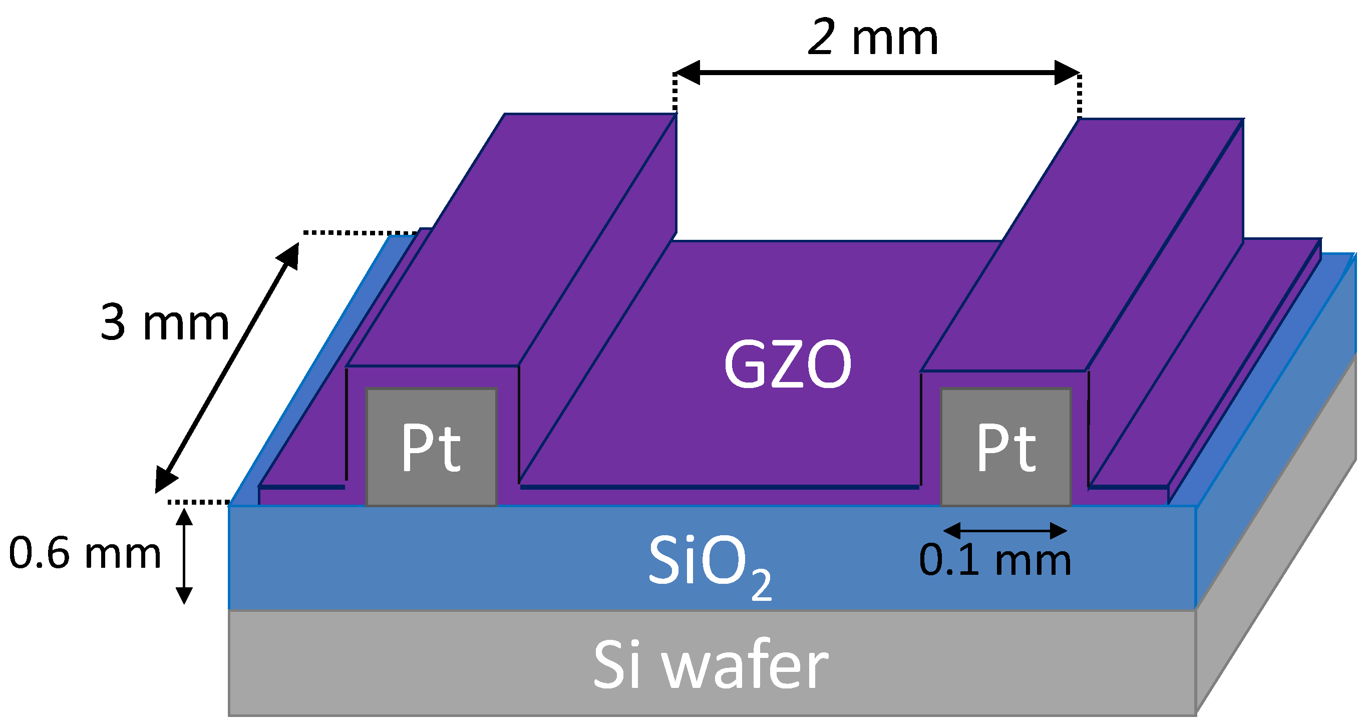
2.1. Preparation of Gas Sensing Elements

Thin films of Ga-doped ZnO (or GZO) were deposited with the RF magnetron sputtering technique (model SCM 400 from ALCATEL CIT) with a magnetron diode configuration. A Zn0.96Ga0.04O ceramic target was used, and the deposition was performed under pure argon atmosphere. The sputtering process parameters are detailed in Table 1.
GZO films of 50 ± 5 nm thickness were deposited using these parameters. The thickness of the films was measured and confirmed using a Dektak 3030ST profilometer (Veeco, Plainview, NY, USA) and the X-ray reflection method using a D8 ADVANCE (Bruker, Billerica, MA, USA) equipped with a LynxEye detector (Bruker, Billerica, MA, USA).
For gas sensing measurement, the films were deposited on test devices (TD). These platforms are made of silicon wafer electrically passivated with a 600 nm thick SiO2 layer obtained by thermal oxidation. Above SiO2 layer were added platinum electrodes (150 nm thick and 100 µm wide), with 3 mm of length, and spaced by 2 mm. For photolithography, a MA/BA6 Gen4 mask aligner (Suss Microtec, Garching near Munich, Germany) was used. The schematic structure of the test vehicle obtained is shown in Figure 1. During GZO deposition, Kapton tape was used to keep the measurement pads uncovered.
After GZO deposition, different samples were annealed in a tubular oven under a dry synthetic air atmosphere for 4 h at 500 °C, 600 °C, or 700 °C. Obtained samples were named according to their annealing temperature: A0, A500, A600, and A700 for samples non-annealed and annealed at 500 °C, 600 °C, and 700 °C, respectively.

2.2. Microstructural and Structural Characterization

The chemical composition of the GZO films was analyzed with the Field Emission Gun Electron Probe MicroAnalyzer (FEG-EPMA) method using a SX FIVE FE (CAMECA, Gennevilliers, France). The measurement was made on 10 different points on a 1 cm2 surface to validate the thin film homogeneity.
Grazing incidence X-ray diffraction (GIXRD) with a 1° incidence angle was used to analyze the structure of the GZO thin film using a D8 ADVANCE (Bruker, Billerica, MA, USA) equipped with a LynxEye detector (Bruker, Billerica, MA, USA).
Scanning Electron Microscopy (SEM) and Transmission Electron Microscopy (TEM) were used to observe the microstructure of the sample. A Focused Ion Beam (FIB) was used to etch away blades from the samples for TEM observations. These observations were made using a Helios 600i (FEI, Hillsboro, OR, USA) equipped with a FEG and a JEM-2100F (JEOL, Tokyo, Japan) equipped with a CMOS RIO16IS 4K*4K camera (Gatan, Pleasanton, CA, USA) and an EDX Ultim Max TEM (Oxford Instruments, Oxfordshire, England) for Energy-Dispersive X-ray spectroscopy. The TEM observations were completed with cartography obtained with the 4D-STEM system STEMx (Gatan, Pleasanton, CA, USA).
Photoluminescence measurements (PL) were performed at 300 K. A 25 mW 325 nm HeCd laser (Kimmon Koha, Tokyo, Japan) was used as the excitation source. The PL emission was collected by a 36 × reflective microscope objective (Newport Corporation-MKS, Andover, MA, USA) and analyzed using a TriVista spectrometer (S&I Spectroscopy & Imaging GmbH, Warstein, Germany). The combination of the BU2 Idus420 detector (Andor Technology, Concord, MA, USA) with a 150 l/mm, 300 nm blazed grating and a 100 µm slit width results in a spectrometer resolution of 0.7 nm. All measured GZO PL spectrums were stable over time, indicating that no laser annealing of the films occurred.

2.3. Gas Sensing

The test bench is composed of a 150 mL commercial gas chamber (Nextron MPS-CHH6) integrating a heating plate (that can heat from ambient to 600 °C) and 6 tip probes. The chemical composition of the gas mixture is controlled in real time through a test bench from Omicron Technologies. This system integrates digital mass flow controllers and electro-valves, and a LabVIEW program manages the test bench. The reference air atmosphere is provided by an air zero generator ZAG7001 (Envea, Poissy, France), and the argon and NO2 are provided by pressurized gas cylinders (Linde Gas, Lyon, France). The NO2 one is a mixture of 1 ppm of NO2 diluted in 5.0 synthetic air (99.999%). In the following, reference air atmosphere designates clean air with 50% relative humidity at room temperature. The gas is humidified by injecting water vapor through a membrane. A humidity probe located at the outlet of the dilution bench, just before the measuring cell, allows the relative humidity value to be regulated continuously. The total gas stream was flowing continuously at 200 standard cubic centimeters per minute (sccm).
The test samples were put into the gas chamber, without light exposition, and linked to a Keithley 2450 source measure unit (SMU). All resistance measurements were made at 250 °C. Every time there is a change in temperature or atmosphere, the adsorption–desorption equilibria are altered, and a stabilization time of 12 h has been applied to ensure that the baseline drift was marginal for all samples. The measurements were made with 3 different current densities: 10, 50, and 100 mA/cm2. No influence of these current densities has been observed on our test devices.

3. Results and Discussion

3.1. Chemical Composition

The FEG-EPMA method was used to measure the chemical composition of the thin films obtained using RF magnetron sputtering. A total of 200 nm thick films were deposited directly on Si wafer substrates, and three of these samples were annealed at 500, 600, or 700 °C.
Table 2 shows concentration measurements obtained from the FEG-EPMA technique. The Ga concentration is measured at 4.2%at in substitution of zinc, and no effect of annealing concentration is observed. A sub-stoichiometry in oxygen is observed, as shown by the calculation of the ratio O/(Zn + Ga). However, this ratio is overestimated because the substrate apparently has been detected by the FEG-EPMA technique, as the Si compound column shows. Since it is hardly possible to completely rid the Si wafer substrate of its nanometric native SiO2 oxide layer, the concentrations of oxygen presented in Table 2 are probably slightly higher than the actual concentration in the GZO film.
After 4 h of annealing, the oxygen concentration of the thin film does not increase. The annealing for 4 h under dry air at these temperatures does not seem to induce an oxidation of the thin film; on the contrary, the relative oxygen concentration decreases, which could be the sign of oxygen diffusion out of the material into the annealing atmosphere at these temperatures.

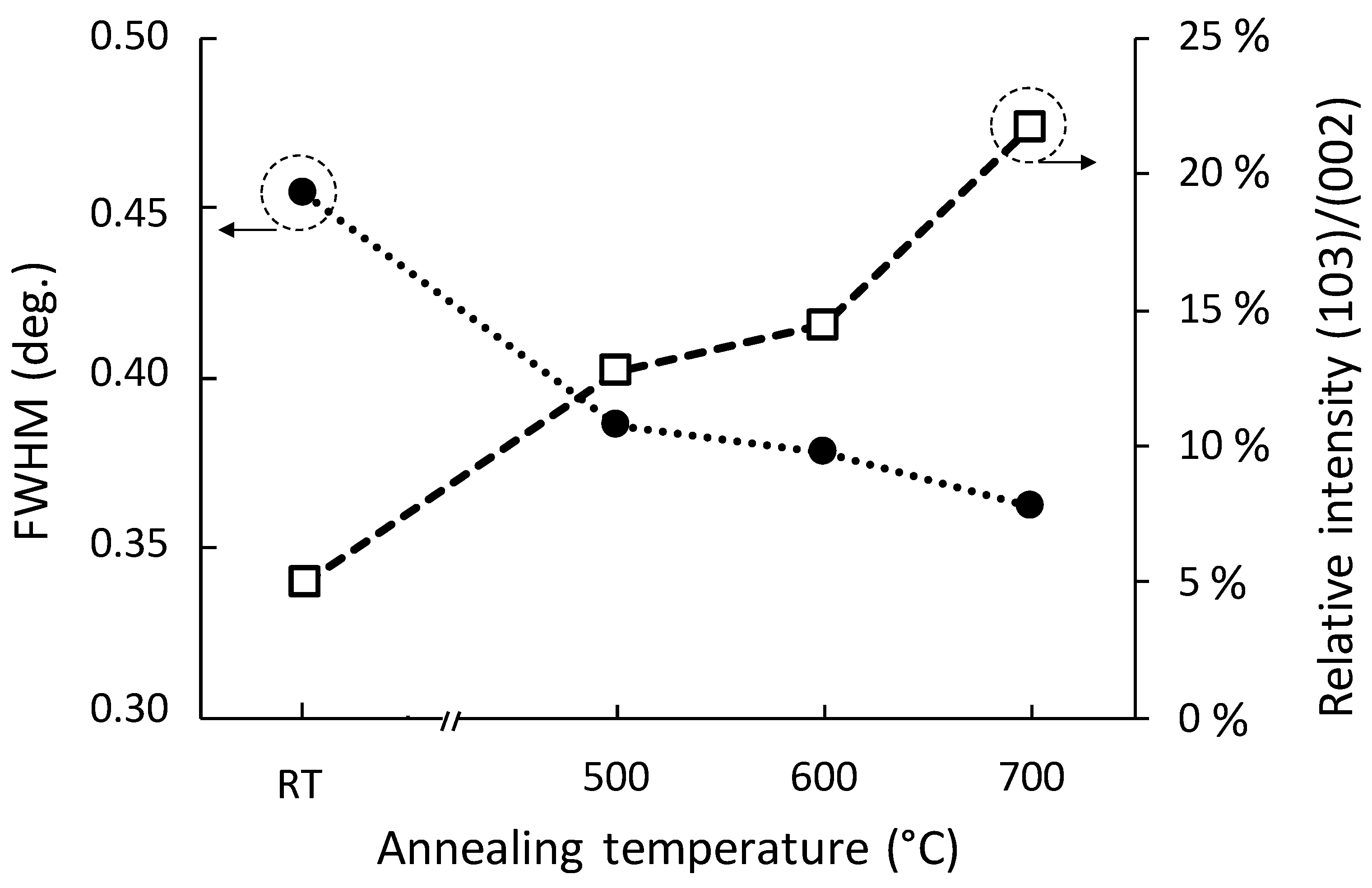
3.2. Influence of Annealing on Film Structure

The diffractograms of the A0, A500, A600, and A700 samples were obtained and are presented in Figure 2.
The diffractogram of the substrate (Si covered by 400 nm of thick SiO2 grown by thermal oxidation) presents large peaks between 15° and 25° and between 50° and 60°, associated with the amorphous SiO2 passivating layer of the substrate and the Si wafer beneath it, respectively (highlighted in light gray domains).
The GZO samples exhibit only two peaks associated with the (002) and (103) planes of the ZnO structure. In reference ZnO crystallographic data [31], the intensities of the (002) and (103) peaks are the 3rd and 5th most intense peaks in the diffractogram, and the intensity ratio between these two peaks is 63%. However, no other diffraction peak is visible, and the highest ratio I(103)/I(002) measured is 22% for A700. This is the sign of an oriented structure of the thin film along the (002) planes. This is consistent with literature for ZnO thin films grown with RF magnetron sputtering [32,33].
A shift towards high angles of these two peaks is observed with increased annealing temperature. Table 3 shows the position of the (002) peak extracted from Figure 2 and the calculated corresponding interplanar distances. These values are compared with reference crystallographic values for ZnO:Ga 4%at.
The as-deposited GZO thin film shows a lower d(002) than the reference, while the corresponding values for A500, A600, and A700 are higher and increase with annealing temperature. This result cannot be explained by the oxygen insertion according to EPMA analysis but by the mechanical stress induced by the substrate. These strains are interpreted as resulting from residual stress along the c-axis. A0 contains compressive residual stress, which probably originates from the deposition process. After annealing, the films contain tensile stress, which increases with annealing temperature. This stress originates from the difference in thermal expansion coefficient of the GZO and the SiO2 substrate [35,36,37].
Figure 3 shows the evolution of the I(103)/I(002) intensity ratio along with the full width at half maximum (FWHM) of the (002) peak as a function of the annealing temperature. The I(103)/I(002) ratio increases with the increase in annealing temperature, a sign of a reorientation of the thin film structure. This specific behavior has already been reported in the literature for ZnO thin films obtained by RF magnetron sputtering and is expected to increase further with annealing temperature over 700 °C [32,33]. In the meantime, the full width at half maximum (FWHM) of the (002) and (103) peaks is decreasing with the increase in the annealing temperature. This is the sign of an improvement of the crystallinity of the thin film, either through the growth or fusion of crystallites or by the disappearance of micro strains in the lattice through the annihilation of crystal defects.
In conclusion, the XRD analyses show that the films present a preferred orientation along the (002) planes parallel to the surface of the substrate. Annealing induces a partial reorientation along the (103) planes of the film structure as well as an improvement of the crystallinity of the thin films; these are more marked as the annealing temperature increases.

3.3. Influence of Annealing on Microstructural Properties

SEM observations of the surface of the films are available in Figure 4. It reveals an equiaxed microstructure. The average grain size of each film has been measured from these images and is presented in Table 4. No significant evolution of the grain size has been observed after annealing; the average value for all films is in between 14 nm and 16 nm. A slight texture change can be noted for A700. These observations are also consistent with what is reported in the literature for ZnO thin films [32,33].
TEM observations of the A0 and A600 samples are presented in Figure 5. The TEM blade thickness being around 100 nm thick and the grain around 15 nm large, the electron beam goes through more than seven different grains on average, making the images difficult to analyze. A columnar microstructure is expected [10,11,33] but difficult to identify in these TEM images.
These TEM images are completed with virtual dark field images obtained with the 4D-STEM mapping system in Figure 6. These images reveal a columnar microstructure of thin films; the height of grains seems equal to the film’s thickness. Grain width measured on these images seems consistent with the SEM observations; however, sampling is too scarce to properly measure the average size of the crystallites composing the grain before and after annealing.
The observed structural orientations are in accordance with the XRD observations. Note that since the diffracted beam probes the thin film along a direction perpendicular to that of the direction probed by the X-ray beam in the XRD experiment, the (002) planes seen in the diffractogram of Figure 2 will appear as (002), planes as well as planes orthogonal to (002) such as (100) and (110) in Figure 6.
From these observations, it is concluded that the films have a columnar microstructure with grains 50 nm high and 15 nm large on average. No significant effect of annealing on grain size was observed.

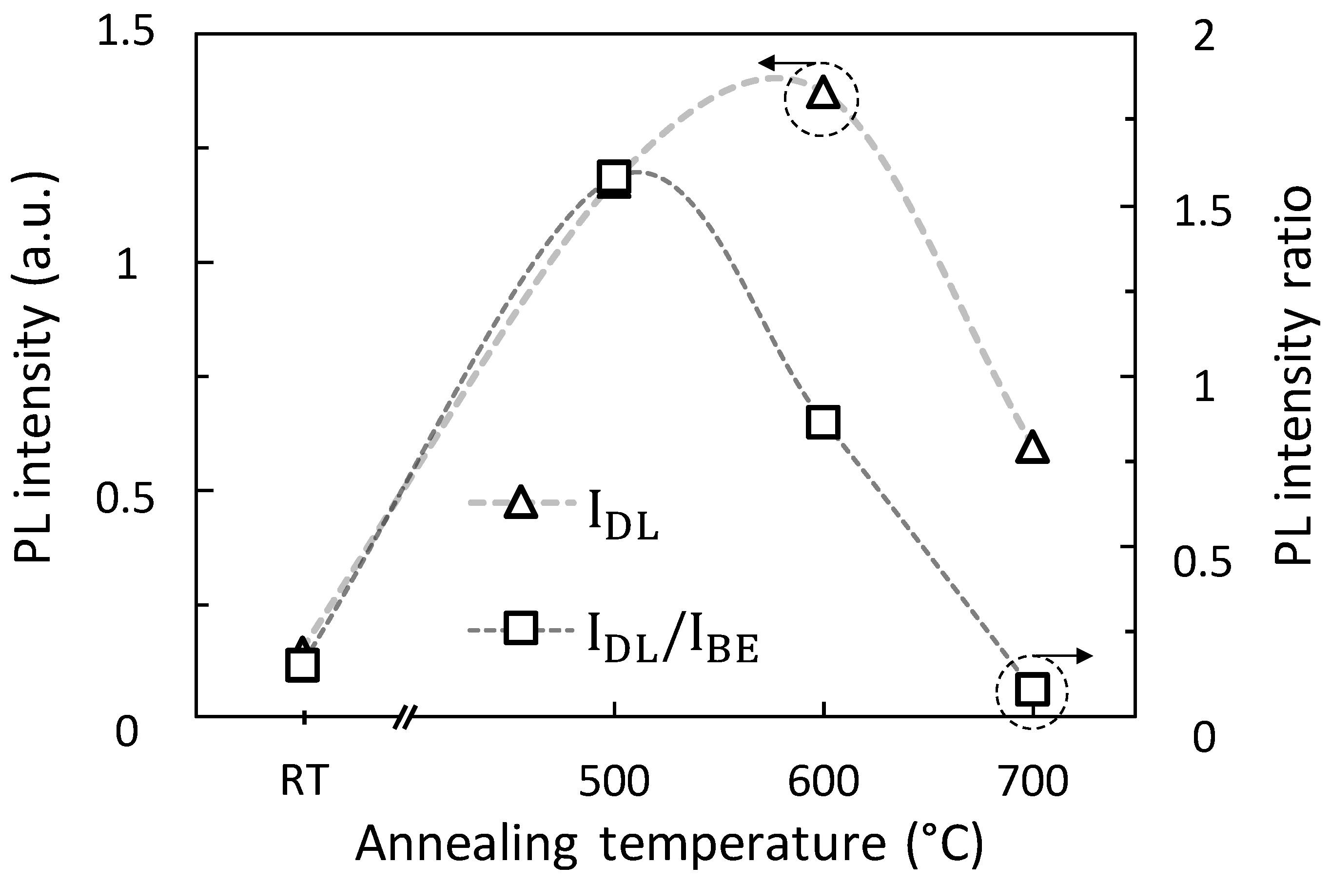
3.4. Photoluminescence Measurements

XRD analysis showed an increase in the crystallinity of the material with annealing, but no grain growth was observed with SEM or TEM. This recrystallization must thus originate from the annihilation of crystal defects. Photoluminescent (PL) was used to study these defects.
The lines of a PL spectrum are associated with material properties (such as the band gap) and crystal defects, but other crystal defects do not appear directly in the spectra in the form of rays. During PL measurement, the electrons excited by the laser will undergo a transition from an excited energy level to another energy level. It will do so either by emitting a photon or a phonon. These two mechanisms are called radiative and non-radiative transitions, respectively [38]. The efficiency of PL emission is defined as the fraction of transitions that are radiative transitions; it can be described by
η = I r I r + I n r ,
where η is the luminescence efficiency, and Ir and Inr are the radiative and non-radiative transition probabilities.
In the case of ZnO, many radiative and non-radiative transitions can be associated with crystal defects. These defects can be referred to either as radiative or non-radiative transition-associated defects (RAD or nRAD, respectively).
Radiative transitions are either associated with the intrinsic properties of the crystalline material, such as its band gap, or to RAD, such as oxygen vacancies VO (deep-level emission ray). The transition probability and thus the PL intensity of a peak is linked to the RAD concentration but also to the radiative transition mechanism.
On the other hand, a large variety of different defects can be an nRA: stacking faults, dislocations, grain boundaries, or even chemisorbed species on the surface [38,39]. Information about their presence and concentration can be extracted using the PL efficiency through a relative comparison of the total PL intensity Itot of each spectrum. An increase in Itot with annealing can be attributed to a diminution of the nRAD concentration.
For PL spectra, 200 nm thick samples were deposited and annealed with parameters comparable to those of 50 nm thick gas sensing samples. These samples were made thicker to improve the signal-to-noise ratio of the spectra measurement, as the vertical step of the focal point of the photoluminescence test bench is 50 nm. Figure 7 shows the photoluminescent (PL) spectrum obtained for these samples.

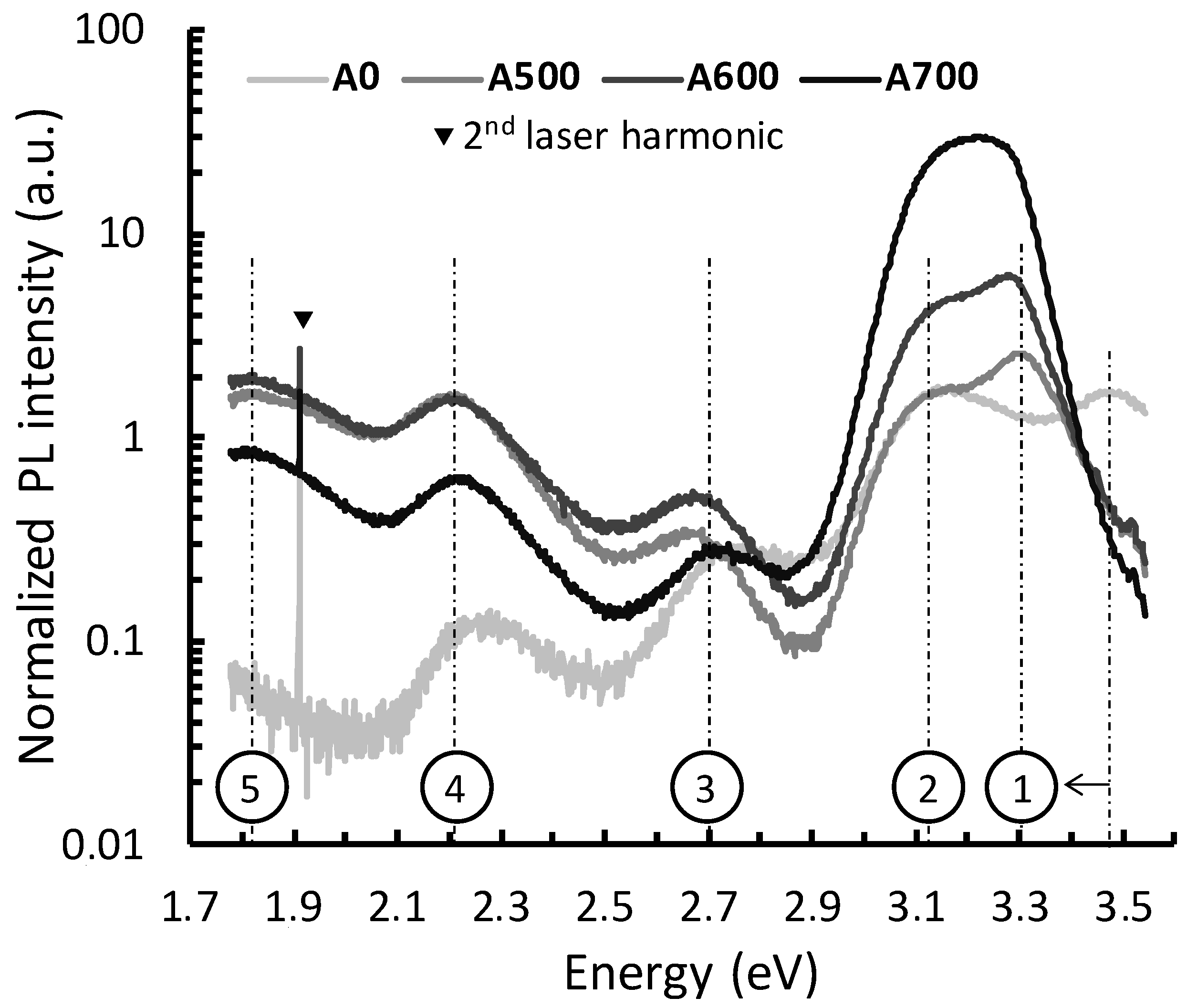
3.4.1. Description and Identification

The spectra show five lines numbered from 1 to 5 in decreasing energy order. They can be divided into two groups: the highest energy rays form the band edge (BE), and the other peaks below 3 eV form the deep levels (DL). Every spectrum has been fitted with five Gaussian curves.
The first line (1) of highest energy is commonly associated with the band gap (BG) transition. For the A0 sample, we observe a 0.2 eV shift in the BG line towards high energy, certainly due to a Burstein–Moss effect [40], which implies that the carrier concentration in the as-deposited layer is particularly high. This effect disappears after annealing, resulting in a band gap of 3.3 eV, as expected of a GZO thin film [23,34,41,42,43,44].
The origin of the four other lines present in the spectra is more difficult to identify and is a subject of controversy in the literature [21,22,23,24,25,26,27]. Such PL spectra lines can be associated with crystal defects in the lattice [22,23], impurities in ZnO [45], or even adsorbed gasses such as oxygen [26] or OH groups [46,47,48,49,50,51]. This is why one must be careful when it comes to such PL line identification.
Since the No. 2 line evolves in a similar way as the BG line with annealing temperature, in opposition to the DL lines, it is associated with a longitudinal optical (LO) phonon replica of the BG transition [29,52,53,54]. It can be noted that other interpretations are available in the literature: zinc interstitial Zni [55], oxygen vacancy VO [22], and Ga doping GaZn [8,56] could also be linked to this BE transition.
The three other DL lines (No. 3, 4, and 5) show very similar behavior with annealing temperature. Table 5 gathers different proposed identifications for lines 3, 4, and 5 available in the literature, putting in first the preferred interpretation in this work.
Three arguments can be proposed to back VO as a crystal defect existing in the GZO thin films: First, the GZO films are poor in oxygen, as the electronic probe results from Table 2 show, thus excluding oxygen-rich defects such as interstitial oxygen. Second, the thermal activation of the mobility of most crystal defects in ZnO is below 300 °C, with the exception of oxygen vacancies charged neutral compared to the lattice V O x , which mobility is activated at 630 °C [23]. All other crystal defects should be at least partially annihilated after annealing except for samples annealed at temperatures higher than 630 °C. Lastly, stacking faults in the ZnO crystal lattice have been reported to transform into VO after annealing [59]. This is consistent with the increase in crystallinity with annealing temperature deduced from the XRD analysis above.
It can be noted that the signature green PL line of ZnO cannot be seen in this study. As this green PL line is often associated with VO, a possible explanation would be that because of the dominance of surface effects and the high Ga doping, the V O + + capture electrons from the material to transform into V O + or V O x , then change the transition energy level of the VO defect [24,28].

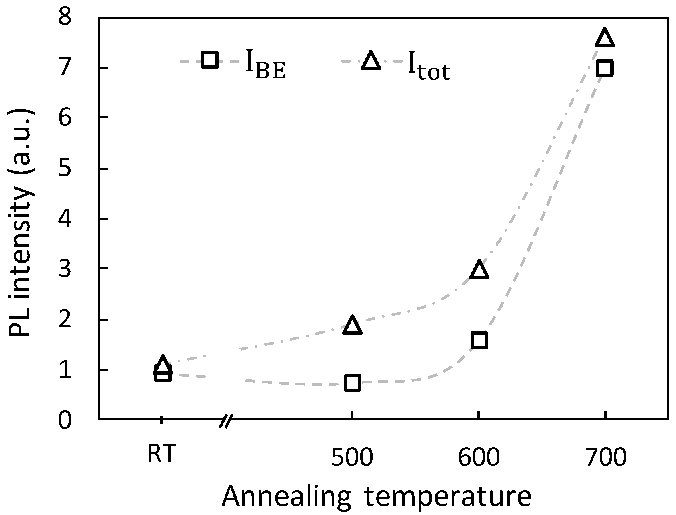
3.4.2. Cristallinity/nRAD

By studying the total PL intensity Itot of each spectrum, the amount of non-radiative transitions is linked to the efficiency of the PL emission, which carries information about non-radiative defects in the material.
Figure 8 shows the evolution with annealing temperature of the total intensity of the spectra Itot and the intensity of the BE lines noted IBE. The values contain information about nRAD concentration.
Intensity of a line is here defined as the area of the Gaussian fit of a line, and the total intensity as the area under the spectrum ray. The total intensity Itot and the intensity of the lines of the spectra can be compared between each other and between spectra since each spectrum is measured in the same conditions and is normalized with the intensity of the laser 2nd harmonic line at 1.91 eV, which depends mostly on the laser and the PL experimental setup and little on the material.
The increase in both Itot and IBE with annealing is a sign of the recrystallization of the film that is consistent with the XRD analysis. An increase of Itot is associated with a decrease in nRAD concentration, while an increase in IBE is associated with a decrease in RAD concentration. Itot increases with any annealing temperature, while IBE only increases for an annealing temperature higher than 600 °C. This shows that the annihilation of nRAD is active at all the studied annealing temperatures while the annihilation of RAD is active only for temperatures above 600 °C. This is consistent with the annihilation temperature of VO, which tends to confirm that the RAD can be associated with VO.
Figure 9 shows the evolution of PL intensity ratio IDL/IBE and of the sum of the intensities of the DL lines IDL as a function of annealing temperature. IDL is directly linked to the PL efficiency and thus to the concentration of the RAD associated with the DL lines. The PL intensity ratio is related to the importance of surface effects in the material [24,28,29,30]. It has been proposed that some radiative transitions need the migration of a hole from the surface of the grain to a RAD. These holes would mostly originate from the chemisorption of oxidizing gasses on the surface of the grains. This implies that the RAD must either be located close to the surface of the grain or that the diffusion depth of the holes in the material is large enough to reach the RAD. In other words, the PL intensity ratio is linked to the depth of the depletion layer and to the concentration of RAD close to the surface.
A0 has low IDL either because of a high concentration of nRAD masking the RAD in the spectrum or because the RAD concentration is low. The Burstein–Moss effect also indicates a high carrier concentration, which could originate from the high defect concentration.
After annealing at 500 °C, DL lines become more intense; however, the IBE barely changes except as the Burstein-Moss effect disappears (the area remains constant). This is interpreted as the elimination of nRAD defects turning into RAD defects such as VO [59]. The highest intensity ratio level is obtained for A500. This sample combines high RAD and nRAD concentrations with the most visible surface effects.
After annealing at 600 °C, Itot increased twice as much as after annealing at 500 °C. This means nRAD defects are annihilated. PL intensity ratio decreases compared to A500, and only a slight increase in IDL is observed. This is found to be the consequence of a further annihilation of nRAD but without much increase in RAD concentration. A600 exhibits the highest RAD concentration as IDL is maximum, and the surface effect seems less important than that of A500.
After annealing at 700 °C, a dramatic increase of Itot is observed, largely more so than for the other samples. In the meantime, IDL is half the value of that of A600. This translates as a clear decrease in both nRAD and RAD concentration. The PL ratio hence surface effects are the lowest of all samples.
To summarize, it is observed that A500 shows the most intense surface effects while A600 has the highest VO concentration.

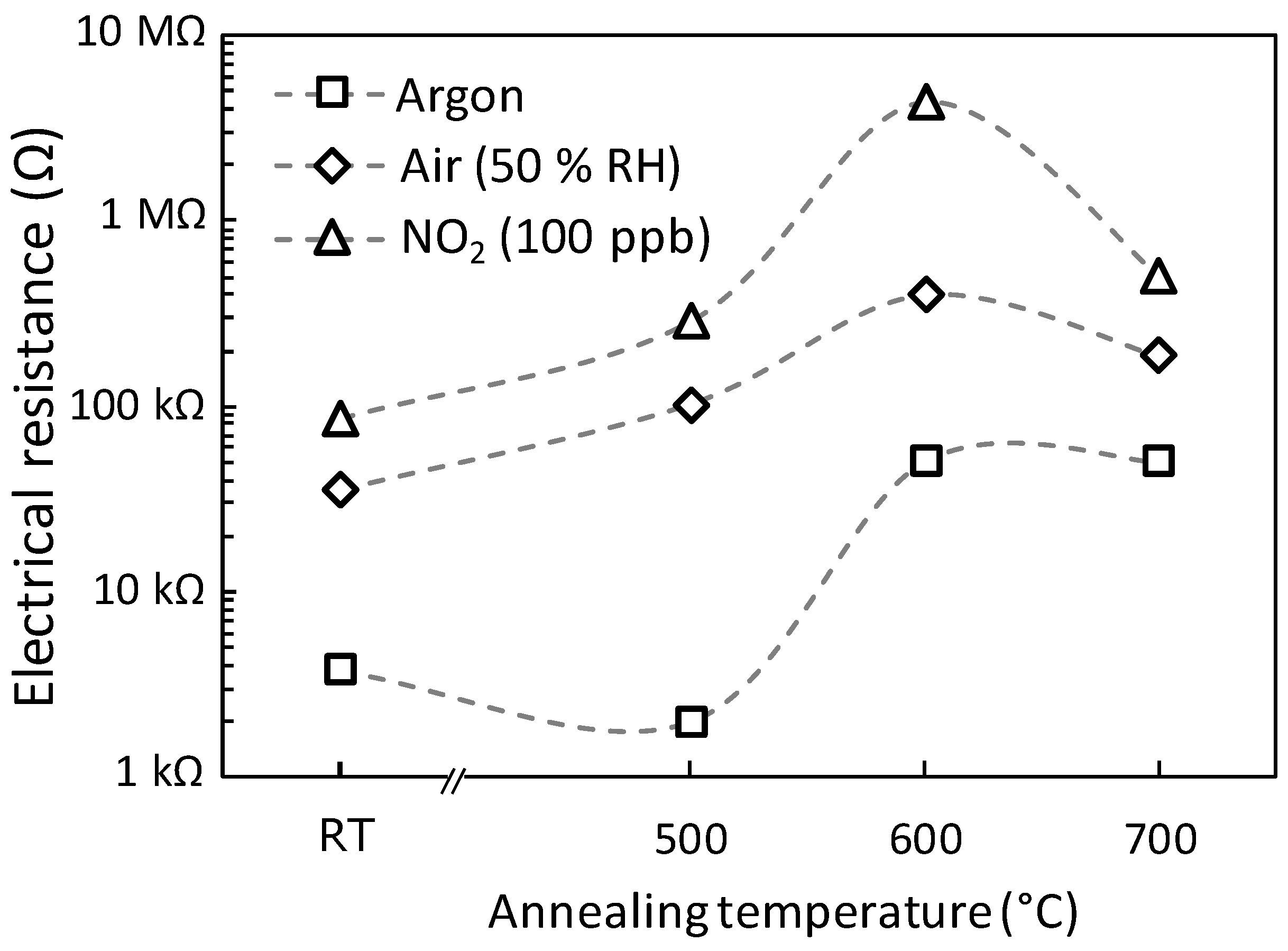
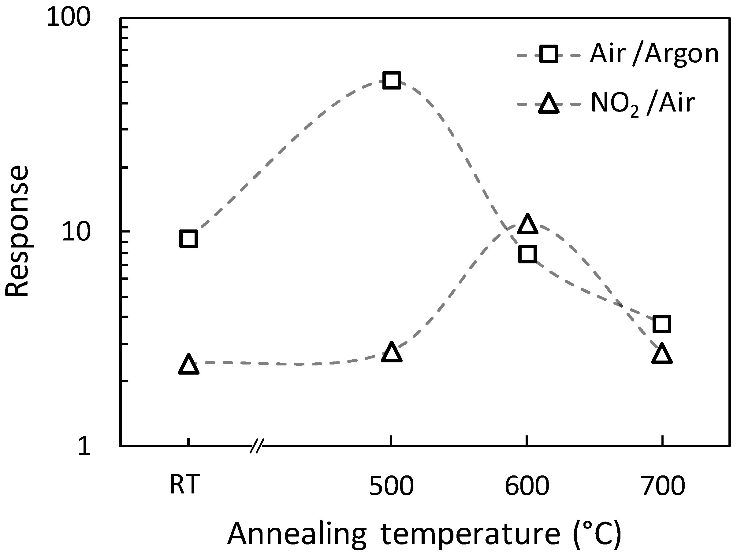
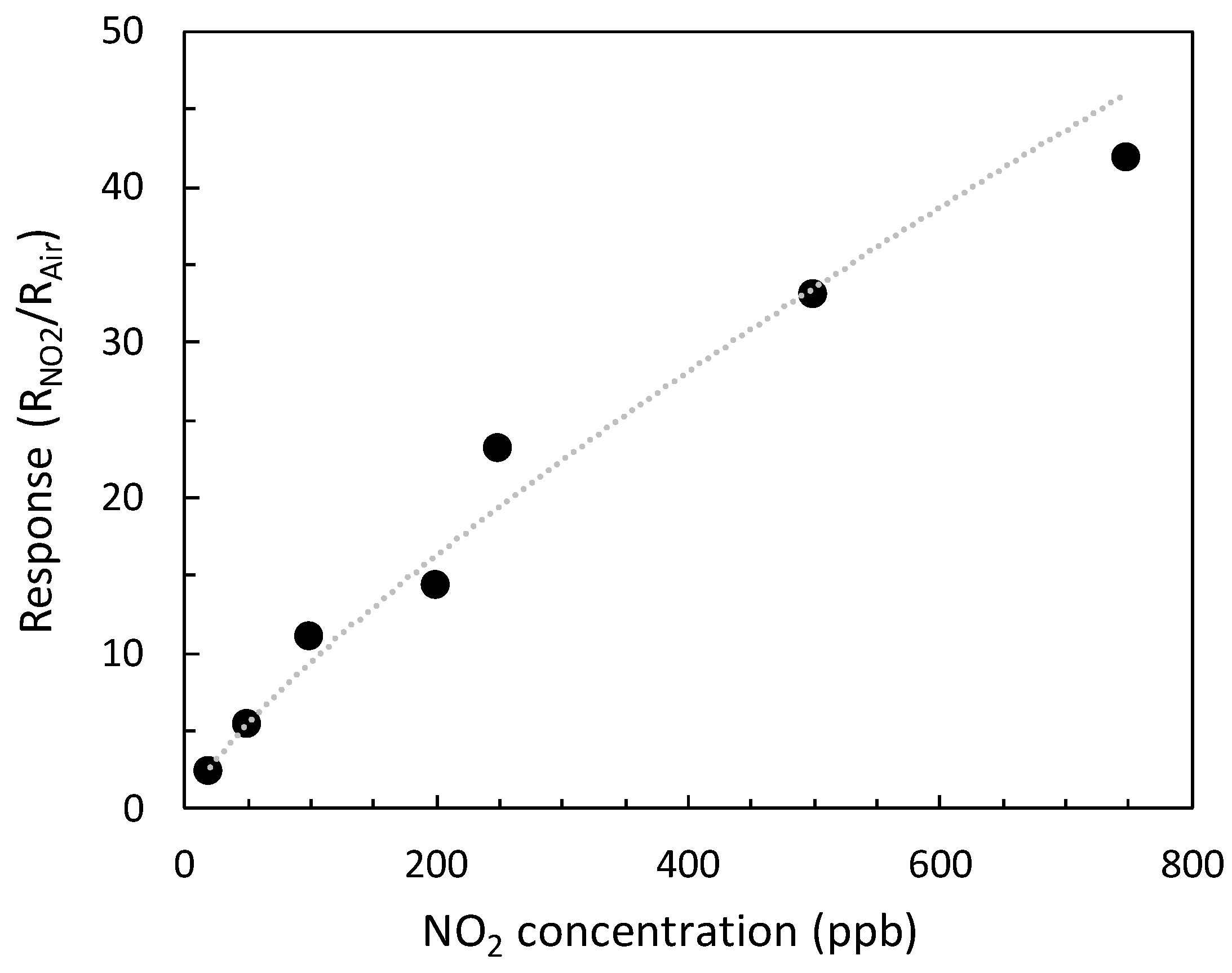
3.5. Gas Sensing Tests and Response to 100 ppb of NO2

The results of this PL analysis are interesting for understanding the evolution of gas sensing properties of these GZO thin films with annealing temperature. There are two main reasons for that: First, it is commonly accepted that the ratio of depletion layer depth to grain size significantly improves gas sensitivity as it increases [5,6]. Second, and more specific to NO2 sensing, VO have been shown to behave as preferential chemisorption sites for NO2 at the surface of ZnO [13,14,15,16,17,18,19,20] compared to other components of the reference atmosphere such as O2, N2, and H2O. Note that VO has been presented as the most probable origin of the RAD in this work.
The electrical resistance of the thin films has been measured under neutral argon atmosphere, humid air as reference atmosphere, and reference atmosphere polluted by 100 ppb of NO2. All measurements were made at 250 °C after 12 h of stabilization. The results are presented in Figure 10.
The resistance measured under a neutral argon atmosphere is a good representation of the intrinsic conductivity of the material since the effect of chemisorption is minimized. A tenfold increase in resistance is observed between A500 and A600. Since no evidence of major microstructural change has been observed, this increase in resistivity should result from a decrease in the density or mobility of charge carriers (which is less likely).
The reduction in charge carriers could be the result of a Ga migration outside the lattice; it could also result from a decrease in shallow defects of donor crystal in GZO, as these defects are often linked to ZnO n-type behavior [23].
On one hand, no sign of Ga precipitation has been observed in XRD nor in TEM analysis. On the other hand, nRAD that could possibly play the role of shallow donors are annihilated for temperatures over 500 °C, as can be deduced from the diminution of the total intensity of the spectra with increased annealing temperatures. However, this wouldn’t explain why both A600 and A700 have the same resistance under argon.
The evolution of resistance between reference air and neutral argon atmosphere, as well as the evolution between polluted atmosphere and reference air, are indicators of the chemisorption reactions of the gasses present in the atmosphere (O2, N2, H2O, and NO2). Reference air atmosphere designates clean air provided by an air zero generator and with relative humidity regulated at 50% at room temperature. As expected, the GZO thin films exhibit n-type behavior, shown by the increase in resistivity as the atmosphere contains more and more oxidizing gasses. In any of the studied atmospheres, A600 manifests the highest resistance, especially under NO200-polluted atmospheres.
Response to air (versus argon) and responses to 100 ppb of NO2 (versus air and versus argon) are here defined as the ratios RAir/RArgon and RNO2/RAir and RNO2/RArgon, respectively, with RArgon, Rair, and RNO2 being the resistance under argon, air (50% RH), and air + 100 ppb of NO2 (50% RH), respectively. These responses are available in Table 6.
The measured responses RNO2/RAir to 100 ppb of NO2 are all higher than 2.4, an interesting performance compared to other ZnO nanomaterials, for most of which the limit of detection is reported to be around a few hundred ppb, except for material with particle size under 50 nm [60]. These results also compare well with other thermally activated GZO works [61,62,63]. As these performances are already competitive, the three-fold increase in response for A600 is of high interest.
Each film except A600 shows a higher sensitivity to humid air than to NO2. A500 shows a remarkable sensitivity to humid air with a response of 51. The response to air decreases with an increase in annealing temperature. A600 exhibits a response of 10.9 to NO2, threefold higher than any of the other samples. A0 has a relatively lower sensitivity to NO2 in regard to the annealed samples.
Figure 11 shows the evolution of the response to air and to NO2 as a function of the annealing temperature. The comparison with Figure 9 shows a rather similar evolution between air response and PL intensity ratio. In the meantime, A600 shows both the highest sensitivity to NO2 and the highest IDL.
Focusing on sensitivity to air (versus argon), the diminution of RAir/RAr with annealing temperature is consistent with the PL results: the surface effects are maximum for A500; hence the general gas sensitivity is maximum as it is controlled by the ratio of depletion layer depth over grain size.
However, the RNO2/RAir is maximum for A600, while A500 and A700 have about the same lower response to NO2. This could be linked to an increase in selectivity towards NO2 rather than a maximization of general gas sensitivity.
When comparing the IDL of A500 and A600, VO concentrations of both samples seemed rather similar, but nRAD concentration was lower for A600 than for A500. It is hypothesized that the higher the fraction of VO defects, the higher the selectivity towards NO2. nRAD defects seem to behave as unspecific chemisorption sites, whereas RAD defects are chemisorption sites with a preferential affinity to NO2.
A700 shows a dramatic decrease in both RAD (VO) and nRAD concentration. This would be understandable since VO are annihilated at temperatures higher than 630 °C [23]. To summarize, annealing at 600 °C allows for a specific annihilation of nRAD defects, increasing the fraction of VO among all the defects present in the material, which in turn leads to an increased sensitivity towards NO2.
Figure 12 allows comparing the results of gas tests of the four samples at 250 °C after a 20 h long stabilization under a reference atmosphere of clean air at 50% HR at room temperature. Six successive injections of 100 ppb of NO2 are generated in the measuring chamber, knowing that each injection lasts 2 h with a return to reference atmosphere for 2 h. The resistance of different samples has been measured at three different current densities: 10, 50, and 100 mA/cm2 in order to evaluate possible influence on the response. No effect of the current density in that range was observed on the electrical response of the GZO thin films except a larger signal noise for the lower current density. The responses RNO2/Rair are given in Table 6. The measured response times for A0, A500, A600, and A700 were 63, 86, 73, and 82 min, respectively. It can be argued that those response times are undervalued since no stability of the resistance under NO2 was achieved at the end of the pulses. This poor response kinetics must be improved to be applied in actual air quality monitoring applications, which could be achieved by decreasing the thickness of the film. Such study is currently in progress.
Figure 13 shows the evolution of response RNO2/RAir for the A600 sample as a function of concentration. A response of 2.4 was measured for 20 ppb. These results prove the great potential of these sensors. No response was observed for either CO2, CO, or CH4, and for some VOCs such as acetone, ethanol, and acetaldehyde, demonstrating very good selectivity of ZnO:Ga thin films for the NO2 detection.

4. Conclusions

The sensitivity of 50 nm thick GZO films grown by RF sputtering was studied. The films were annealed under dry air for 4 h at either 500 °C, 600 °C, or 700 °C. A threefold increase in sensitivity to NO2 is observed only for samples annealed at 600 °C. To understand this phenomenon, photoluminescence spectra of 4 films before and after annealing were compared with their electrical resistance at 250 °C under neutral argon atmosphere, humid air reference atmosphere, and reference atmosphere polluted by 100 ppb of NO2. It has been concluded that annealing at 600 °C resulted in a specific annihilation of non-radiative defects, an increase in the proportions of VO defects, which certainly play the predominant role of NO2-specific chemisorption sites. Annealing at 700 °C resulted in a non-specific annihilation of all crystal defects; thus, a significant decrease in NO2 sensitivity was observed that confirmed the role of these defects in gas detection. Interestingly, 600 °C appears to be an optimum annealing temperature in these conditions; further experiments with intermediary temperatures could be useful to more precisely identify this optimum temperature. Furthermore, as the proposed mechanism relies on a specific annihilation of defect active at certain temperatures, increasing the annealing duration should further increase the relative concentration of VO and thus further improve sensitivity to NO2.
A gas sensor with promising performances at the ppb level was achieved using an easily industrializable process and cheap materials, even though its response time should be improved. A solution could be found by improving the accessibility of the surface to gasses, by decreasing the film’s thickness, for example.
Although similar works have shown an improvement of gas sensing properties of GZO thin films with annealing at specific temperatures, no interpretation of this phenomenon had been proposed [64].
This annealing optimization should prove to be an interesting process to improve existing ZnO-based resistive gas sensors and be useful for metal oxide gas sensors in general.

Author Contributions

Investigation and writing by B.P.; validation and supervision by L.P. and P.M.; material and electrical characterization support by A.B., Y.T., T.C. and R.M. All authors have read and agreed to the published version of the manuscript.

Funding

This research was funded by Agence Nationale de la Recherche, grant number ANR-20-CE04-0012. This work was supported by the LAAS-CNRS micro and nanotechnologies platform, a member of the French Renatech network.

Institutional Review Board Statement

Not applicable.

Informed Consent Statement

Not applicable.

Data Availability Statement

The data presented in this study are available on request from the corresponding author.

Acknowledgments

The authors thank the Centre de microcaractérisation Raimond Castaing of Toulouse, where microstructural characterization has been carried out.

Conflicts of Interest

The authors declare no conflicts of interest.

References

  1. Choudhari, U.; Jagtap, S. A Panoramic View of NOx and NH3 Gas Sensors. Nano-Struct. Nano-Objects 2023, 35, 100995. [Google Scholar] [CrossRef]
  2. Ji, H.; Zeng, W.; Li, Y. Gas Sensing Mechanisms of Metal Oxide Semiconductors: A Focus Review. Nanoscale 2019, 11, 22664–22684. [Google Scholar] [CrossRef]
  3. Kumar, R.; Al-Dossary, O.; Kumar, G.; Umar, A. Zinc Oxide Nanostructures for NO2 Gas–Sensor Applications: A Review. Nano-Micro Lett. 2015, 7, 97–120. [Google Scholar] [CrossRef] [PubMed]
  4. Franco, M.A.; Conti, P.P.; Andre, R.S.; Correa, D.S. A Review on Chemiresistive ZnO Gas Sensors. Sens. Actuators Rep. 2022, 4, 100100. [Google Scholar] [CrossRef]
  5. Rothschild, A.; Komem, Y. The Effect of Grain Size on the Sensitivity of Nanocrystalline Metal-Oxide Gas Sensors. J. Appl. Phys. 2004, 95, 6374–6380. [Google Scholar] [CrossRef]
  6. Yamazoe, N.; Sakai, G.; Shimanoe, K. Oxide Semiconductor Gas Sensors. Catal. Surv. Asia. 2003, 7, 63–75. [Google Scholar] [CrossRef]
  7. Ellmer, K. Resistivity of Polycrystalline Zinc Oxide Films: Current Status and Physical Limit. J. Phys. D Appl. Phys. 2001, 34, 3097. [Google Scholar] [CrossRef]
  8. Demchenko, D.O.; Earles, B.; Liu, H.Y.; Avrutin, V.; Izyumskaya, N.; Özgür, Ü.; Morkoç, H. Impurity Complexes and Conductivity of Ga-Doped ZnO. Phys. Rev. B 2011, 84, 075201. [Google Scholar] [CrossRef]
  9. Wang, T.; Chen, J.; Chen, J.; Yao, X.; Chen, G.; Jiao, Z.; Zhao, J.-T.; Cheng, S.; Yang, X.-C.; Li, Q. UV-Light Enhanced Gas Sensor Based on Ga Doped ZnO for Ultra-High Sensitive and Selective n-Butanol Detection. Appl. Surf. Sci. 2023, 641, 158551. [Google Scholar] [CrossRef]
  10. Anders, A. A Structure Zone Diagram Including Plasma-Based Deposition and Ion Etching. Thin Solid Films 2010, 518, 4087–4090. [Google Scholar] [CrossRef]
  11. Gunasekaran, V. Intégration et Caractérisation de Couches Sensibles de ZnO:Ga et de Cobaltites Spinelles (CoxFe3-xO4; 1<=x<=3) Sur Véhicules de Test Pour La Détection de Dioxyde d’azote Sub-ppm et d’éthanol. Ph.D. Thesis, Université de Toulouse, Université Toulouse III—Paul Sabatier, Toulouse, France, 2021. Available online: https://theses.fr/2021TOU30105 (accessed on 1 November 2024).
  12. Yoboué, P.; Konaté, A.; Asseu, O.; Menini, P. An Industrializable Silicon-Based Microhotplate for Metal Oxides Gas Sensors. Phys. Chem. News 2014, 72, 34–41. [Google Scholar]
  13. Quy, C.; Thai, N.; Duc Hoa, N.; Thi Thanh Le, D.; Hung, C.; Duy, N.; Hieu, N. C2H5OH and NO2 Sensing Properties of ZnO Nanostructures: Correlation between Crystal Size, Defect Level and Sensing Performance. RSC Adv. 2018, 8, 5629–5639. [Google Scholar] [CrossRef] [PubMed]
  14. Li, G.; Zhang, H.; Meng, L.; Sun, Z.; Chen, Z.; Huang, X.; Qin, Y. Adjustment of Oxygen Vacancy States in ZnO and Its Application in Ppb-Level NO2 Gas Sensor. Sci. Bull. 2020, 65, 1650–1658. [Google Scholar] [CrossRef] [PubMed]
  15. Yu, L.; Guo, F.; Liu, S.; Yang, B.; Jiang, Y.; Qi, L.; Fan, X. Both Oxygen Vacancies Defects and Porosity Facilitated NO2 Gas Sensing Response in 2D ZnO Nanowalls at Room Temperature. J. Alloy Compd. 2016, 682, 352–356. [Google Scholar] [CrossRef]
  16. Kumar, R.R.; Murugesan, T.; Chang, T.-W.; Lin, H.-N. Defect Controlled Adsorption/Desorption Kinetics of ZnO Nanorods for UV-Activated NO2 Gas Sensing at Room Temperature. Mater. Lett. 2021, 287, 129257. [Google Scholar] [CrossRef]
  17. Zhang, C.; Geng, X.; Li, J.; Luo, Y.; Lu, P. Role of Oxygen Vacancy in Tuning of Optical, Electrical and NO2 Sensing Properties of ZnO1-x Coatings at Room Temperature. Sens. Actuat. B-Chem. 2017, 248, 886–893. [Google Scholar] [CrossRef]
  18. Sundara Venkatesh, P.; Dharmaraj, P.; Purushothaman, V.; Ramakrishnan, V.; Jeganathan, K. Point Defects Assisted NH3 Gas Sensing Properties in ZnO Nanostructures. Sens. Actuat. B-Chem. 2015, 212, 10–17. [Google Scholar] [CrossRef]
  19. Spencer, M.J.S.; Yarovsky, I. ZnO Nanostructures for Gas Sensing: Interaction of NO2, NO, O, and N with the ZnO( 10 10 - ) Surface. J. Phys. Chem. C 2010, 114, 10881–10893. [Google Scholar] [CrossRef]
  20. An, W.; Wu, X.; Zeng, X.C. Adsorption of O2, H2, CO, NH3, and NO2 on ZnO Nanotube:  A Density Functional Theory Study. J. Phys. Chem. C 2008, 112, 5747–5755. [Google Scholar] [CrossRef]
  21. Djurisic, A.; Leung, Y.; Tam, K.; Ding, L.; Ge, W.; Chen, H.-Y.; Gwo, S. Green, Yellow, and Orange Defect Emission from ZnO Nanostructures: Influence of Excitation Wavelength. Appl. Phys. Lett. 2006, 88, 103107. [Google Scholar] [CrossRef]
  22. Lyons, J.L.; Varley, J.B.; Steiauf, D.; Janotti, A.; Van de Walle, C.G. First-Principles Characterization of Native-Defect-Related Optical Transitions in ZnO. J. Appl. Phys. 2017, 122, 035704. [Google Scholar] [CrossRef]
  23. Janotti, A.; Van De Walle, C.G. Fundamentals of Zinc Oxide as a Semiconductor. Rep. Prog. Phys. 2009, 72, 126501. [Google Scholar] [CrossRef]
  24. Vanheusden, K.; Warren, W.L.; Seager, C.H.; Tallant, D.R.; Voigt, J.A.; Gnade, B.E. Mechanisms behind Green Photoluminescence in ZnO Phosphor Powders. J. Appl. Phys. 1996, 79, 7983–7990. [Google Scholar] [CrossRef]
  25. Lin, B.; Fu, Z.; Jia, Y. Green Luminescent Center in Undoped Zinc Oxide Films Deposited on Silicon Substrates. Appl. Phys. Lett. 2001, 79, 943–945. [Google Scholar] [CrossRef]
  26. Röhr, J.A.; Sá, J.; Konezny, S.J. The Role of Adsorbates in the Green Emission and Conductivity of Zinc Oxide. Commun. Chem. 2019, 2, 52. [Google Scholar] [CrossRef]
  27. Özgür, Ü.; Alivov, Y.I.; Liu, C.; Teke, A.; Reshchikov, M.A.; Doǧan, S.; Avrutin, V.; Cho, S.J.; Morkç, H. A Comprehensive Review of ZnO Materials and Devices. J. Appl. Phys. 2005, 98, 041301. [Google Scholar] [CrossRef]
  28. Liao, Z.-M.; Zhang, H.-Z.; Zhou, Y.-B.; Xu, J.; Zhang, J.-M.; Yu, D.-P. Surface Effects on Photoluminescence of Single ZnO Nanowires. Phys. Lett. A 2008, 372, 4505–4509. [Google Scholar] [CrossRef]
  29. Matsumoto, T.; Kato, H.; Miyamoto, K.; Sano, M.; Zhukov, E.A.; Yao, T. Correlation between Grain Size and Optical Properties in Zinc Oxide Thin Films. Appl. Phys. Lett. 2002, 81, 1231–1233. [Google Scholar] [CrossRef]
  30. Shalish, I.; Temkin, H.; Narayanamurti, V. Size-Dependent Surface Luminescence in ZnO Nanowires. Phys. Rev. B 2004, 69, 245401. [Google Scholar] [CrossRef]
  31. Sawada, H.; Wang, R.; Sleight, A.W. An Electron Density Residual Study of Zinc Oxide. J. Solid State Chem. 1996, 122, 148–150. [Google Scholar] [CrossRef]
  32. Bura, M.; Singh, G.; Gupta, D.; Malik, N.; Salim, A.; Kumar, A.; Singhal, R.; Kumar, S.; Aggarwal, S. Transition in the Preferred Orientation of RF Sputtered ZnO/Si Thin Films by Thermal Annealing: Structural, Morphological, and Optical Characteristics. Opt. Mater. 2022, 133, 113024. [Google Scholar] [CrossRef]
  33. Gupta, V.; Mansingh, A. Influence of Postdeposition Annealing on the Structural and Optical Properties of Sputtered Zinc Oxide Film. J. Appl. Phys. 1996, 80, 1063–1073. [Google Scholar] [CrossRef]
  34. Gonçalves, G.; Elamurugu, E.; Barquinha, P.; Pereira, L.; Martins, R.; Fortunato, E. Influence of Post-Annealing Temperature on the Properties Exhibited by ITO IZO and GZO Thin Films. Thin Solid Films 2007, 515, 8562–8566. [Google Scholar] [CrossRef]
  35. Valdez, L.A.; Caravaca, M.A.; Casali, R.A. Ab-Initio Study of Elastic Anisotropy, Hardness and Volumetric Thermal Expansion Coefficient of ZnO, ZnS, ZnSe in Wurtzite and Zinc Blende Phases. J. Phys. Chem. Solids 2019, 134, 245–254. [Google Scholar] [CrossRef]
  36. Watanabe, H.; Yamada, N.; Okaji, M. Linear Thermal Expansion Coefficient of Silicon from 293 to 1000 K. Int. J. Thermophys. 2004, 25, 221–236. [Google Scholar] [CrossRef]
  37. Ibach, H. Thermal Expansion of Silicon and Zinc Oxide (II). Phys. Status Solidi B 1969, 33, 257–265. [Google Scholar] [CrossRef]
  38. Van Dijken, A.; Meulenkamp, E.A.; Vanmaekelbergh, D.; Meijerink, A. The Luminescence of Nanocrystalline ZnO Particles: The Mechanism of the Ultraviolet and Visible Emission. J. Lumin. 2000, 87–89, 454–456. [Google Scholar] [CrossRef]
  39. Wang, Y.G.; Lau, S.P.; Lee, H.W.; Yu, S.F.; Tay, B.K.; Zhang, X.H.; Hng, H.H. Photoluminescence Study of ZnO Films Prepared by Thermal Oxidation of Zn Metallic Films in Air. J. Appl. Phys. 2003, 94, 354–358. [Google Scholar] [CrossRef]
  40. Burstein, E. Anomalous Optical Absorption Limit in InSb. Phys. Rev. 1954, 93, 632–633. [Google Scholar] [CrossRef]
  41. Shan, F.K.; Liu, G.X.; Lee, W.J.; Shin, B.C.; Kim, S.C. Nanoscale Phenomena of Gallium-Doped ZnO Thin Films on Sapphire Substrates. J. Electroceram. 2006, 17, 287–292. [Google Scholar] [CrossRef]
  42. Wang, L.-W.; Chu, S.-Y. Effects of Post-Annealing on the Properties of ZnO:Ga Films with High Transparency (94%) and Low Sheet Resistance (29 Ω/Square). Materials 2023, 16, 6463. [Google Scholar] [CrossRef] [PubMed]
  43. Sim, K.U.; Shin, S.W.; Moholkar, A.V.; Yun, J.H.; Moon, J.H.; Kim, J.H. Effects of Dopant (Al, Ga, and In) on the Characteristics of ZnO Thin Films Prepared by RF Magnetron Sputtering System. Curr. Appl. Phys. 2010, 10, S463–S467. [Google Scholar] [CrossRef]
  44. Du Ahn, B.; Hoon Oh, S.; Hee Lee, C.; Hee Kim, G.; Jae Kim, H.; Yeol Lee, S. Influence of Thermal Annealing Ambient on Ga-Doped ZnO Thin Films. J. Cryst. Growth 2007, 309, 128–133. [Google Scholar] [CrossRef]
  45. McCluskey, M.D.; Corolewski, C.D.; Lv, J.; Tarun, M.C.; Teklemichael, S.T.; Walter, E.D.; Norton, M.G.; Harrison, K.W.; Ha, S. Acceptors in ZnO. J. Appl. Phys. 2015, 117, 112802. [Google Scholar] [CrossRef]
  46. Willander, M.; Nur, O.; Sadaf, J.R.; Qadir, M.I.; Zaman, S.; Zainelabdin, A.; Bano, N.; Hussain, I. Luminescence from Zinc Oxide Nanostructures and Polymers and Their Hybrid Devices. Materials 2010, 3, 2643–2667. [Google Scholar] [CrossRef]
  47. Gupta, H.; Singh, J.; Dutt, R.N.; Ojha, S.; Kar, S.; Kumar, R.; Reddy, V.R.; Singh, F. Defect-Induced Photoluminescence from Gallium-Doped Zinc Oxide Thin Films: Influence of Doping and Energetic Ion Irradiation. Phys. Chem. Chem. Phys. 2019, 21, 15019–15029. [Google Scholar] [CrossRef] [PubMed]
  48. Tam, K.H.; Cheung, C.K.; Leung, Y.H.; Djurišić, A.B.; Ling, C.C.; Beling, C.D.; Fung, S.; Kwok, W.M.; Chan, W.K.; Phillips, D.L.; et al. Defects in ZnO Nanorods Prepared by a Hydrothermal Method. J. Phys. Chem. B 2006, 110, 20865–20871. [Google Scholar] [CrossRef]
  49. Baek, M.; Kim, D.; Yong, K. Simple but Effective Way To Enhance Photoelectrochemical Solar-Water-Splitting Performance of ZnO Nanorod Arrays: Charge-Trapping Zn(OH)2 Annihilation and Oxygen Vacancy Generation by Vacuum Annealing. ACS Appl. Mater. Inter. 2017, 9, 2317–2325. [Google Scholar] [CrossRef]
  50. Xie, R.; Li, D.; Yang, D.; Sekiguchi, T.; Jiang, M. Thermal-Desorption Induced Enhancement and Patterning of Ultraviolet Emission in Chemically Grown ZnO. Nanotechnology 2006, 17, 2789. [Google Scholar] [CrossRef]
  51. Djurišić, A.B.; Leung, Y.H.; Tam, K.H.; Hsu, Y.F.; Ding, L.; Ge, W.K.; Zhong, Y.C.; Wong, K.S.; Chan, W.K.; Tam, H.L.; et al. Defect Emissions in ZnO Nanostructures. Nanotechnology 2007, 18, 095702. [Google Scholar] [CrossRef]
  52. Meyer, B.K.; Sann, J.; Hofmann, D.M.; Neumann, C.; Zeuner, A. Shallow Donors and Acceptors in ZnO. Semicond. Sci. Technol. 2005, 20, S62. [Google Scholar] [CrossRef]
  53. Shan, W.; Walukiewicz, W.; Ager, J.W., III; Yu, K.M.; Yuan, H.B.; Xin, H.P.; Cantwell, G.; Song, J.J. Nature of Room-Temperature Photoluminescence in ZnO. Appl. Phys. Lett. 2005, 86, 191911. [Google Scholar] [CrossRef]
  54. Teklemichael, S.T.; McCluskey, M.D. Acceptor and Surface States of ZnO Nanocrystals: A Unified Model. Nanotechnology 2011, 22, 475703. [Google Scholar] [CrossRef] [PubMed]
  55. Chen, M.; Wang, Z.; Han, D.; Gu, F.; Guo, G. Porous ZnO Polygonal Nanoflakes: Synthesis, Use in High-Sensitivity NO2 Gas Sensor, and Proposed Mechanism of Gas Sensing. J. Phys. Chem. C 2011, 115, 12763–12773. [Google Scholar] [CrossRef]
  56. Lee, Y.-S.; Peng, Y.-C.; Lu, J.-H.; Zhu, Y.-R.; Wu, H.-C. Electronic and Optical Properties of Ga-Doped ZnO. Thin Solid Films 2014, 570, 464–470. [Google Scholar] [CrossRef]
  57. Alvi, N.H.; ul Hasan, K.; Nur, O.; Willander, M. The Origin of the Red Emission in n-ZnO Nanotubes/p-GaN White Light Emitting Diodes. Nanoscale Res. Lett. 2011, 6, 130. [Google Scholar] [CrossRef]
  58. Kumar, V.; Swart, H.; Ntwaeaborwa, O.; Kroon, R.; Terblans, J.; Shaat, S.; Mohmmed, A.; Duvenhage, M.-M. Origin of the Red Emission in Zinc Oxide Nanophosphors. Mater. Lett. 2013, 101, 57. [Google Scholar] [CrossRef]
  59. Zhu, Y.; Zhang, X.; Li, R.; Li, Q. Planar-Defect-Rich Zinc Oxide Nanoparticles Assembled on Carbon Nanotube Films as Ultraviolet Emitters and Photocatalysts. Sci. Rep. 2014, 4, 4728. [Google Scholar] [CrossRef]
  60. Van Duy, L.; Nguyet, T.T.; Hung, C.M.; Thanh Le, D.T.; Van Duy, N.; Hoa, N.D.; Biasioli, F.; Tonezzer, M.; Di Natale, C. Ultrasensitive NO2 Gas Sensing Performance of Two Dimensional ZnO Nanomaterials: Nanosheets and Nanoplates. Ceram. Int. 2021, 47, 28811–28820. [Google Scholar] [CrossRef]
  61. Patil, V.L.; Bhosale, S.R.; Bhosale, R.R.; Tarwal, N.L.; Vanalakar, S.A.; Dhavale, R.P.; Sharma, K.K.; Patil, P.S. Low Temperature Chemiresistive Gas Sensing Performance towards Oxidising Gas Based on Chemically Prepared Ga Doped ZnO Nanorods. Inorg. Chem. Commun. 2023, 152, 110691. [Google Scholar] [CrossRef]
  62. Vorobyeva, N.; Rumyantseva, M.; Filatova, D.; Spiridonov, F.; Zaytsev, V.; Zaytseva, A.; Gaskov, A. Highly Sensitive ZnO(Ga,In) for Sub-ppm Level NO2 Detection: Effect of Indium Content. Chemosensors 2017, 5, 18. [Google Scholar] [CrossRef]
  63. Rigon, M.; Paolucci, V.; Sturaro, M.; Emamjomeh, S.M.; Cantalini, C.; Martucci, A. Effect of Pt Nanoparticles on the Plasmonic and Chemoresistive Gas Sensing Properties of ZnO:Ga Film. Proceedings 2018, 2, 997. [Google Scholar] [CrossRef]
  64. Ramola, R.C.; Negi, S.; Rawat, M.; Singh, R.C.; Singh, F. Annealing Effects on Gas Sensing Response of Ga-Doped ZnO Thin Films. ACS Omega 2021, 6, 11660–11668. [Google Scholar] [CrossRef]
Figure 1. Schematic representation of the gas sensing test vehicles, not to scale.
Chemosensors 13 00001 g001
Figure 2. Diffractograms of non-annealed and annealed GZO thin films and of the substrate as a reference.
Chemosensors 13 00001 g002
Figure 3. Evolution of the FWHM of the (002) peak and of the intensity ratio I(103)/I(002) as a function of the annealing temperature.
Chemosensors 13 00001 g003
Figure 4. SEM micrography of thin films, non-annealed and annealed at various temperatures.
Chemosensors 13 00001 g004
Figure 5. TEM micrography of a non-annealed film and a film annealed at 600 °C.
Chemosensors 13 00001 g005
Figure 6. 4D-STEM virtual dark field images.
Chemosensors 13 00001 g006
Figure 7. PL spectrum of non-annealed and annealed GZO thin films, the PL intensity is in log scale.
Chemosensors 13 00001 g007
Figure 8. Evolution of band edge intensity IBE and total intensity of the spectra Itot.
Chemosensors 13 00001 g008
Figure 9. PL intensity ratio and sum of the DL lines’ intensity as a function of the annealing temperature.
Chemosensors 13 00001 g009
Figure 10. Resistance of a GZO thin film at 250 °C as a function of the atmosphere and the annealing temperature.
Chemosensors 13 00001 g010
Figure 11. Response to air and to NO2 in logarithmic scale as a function of the annealing temperature.
Chemosensors 13 00001 g011
Figure 12. Sensing test of different samples under successive injections of 100 ppb of NO2. in reference atmosphere. Electrical resistances were measured with different current densities: 100 mA/cm2 for pulses 1 and 4, 10 mA/cm2 for pulses 2 and 5, and 1 mA/cm2 for pulses 3 and 6.
Chemosensors 13 00001 g012
Figure 13. Response as a function of NO2 concentration measured on the A600 sample.
Chemosensors 13 00001 g013
Table 1. Deposition parameters of GZO thin film by RF magnetron sputtering.
Deposition ParametersValue
Target materialZnO:Ga (4%at)
Power per surface unit1.14 W/cm2
MagnetronYes
Argon pressure2 Pa
Target to substrate distance7 cm
Mean free path0.3 cm
Deposition speed2 nm/min
Table 2. Composition of 200 nm thick films before and after annealing, obtained by an electron probe, in atomic percentage.
Sample
Name
Atomic Concentration (%)
OZnGaSiO/(Zn + Ga)
A049.00 ± 0.0347.58 ± 0.052.18 ± 0.011.25 ± 0.050.985 ± 0.002
A50048.58 ± 0.0347.99 ± 0.032.18 ± 0.011.25 ± 0.060.968 ± 0.001
A60048.61 ± 0.0747.50 ± 0.042.17 ± 0.011.73 ± 0.090.979 ± 0.002
A70048.37 ± 0.0248.17 ± 0.042.20 ± 0.011.26 ± 0.050.960 ± 0.001
Table 3. Position of the (002) peak and associated interplanar distance of the studied samples compared to that of a reference ZnO:Ga 4%at from A. de Souza Gonçalves et al. [34].
Sample Name2θ (002) (°)d(002) (Å)
ZnO:Ga 4%at reference [34] 2.602
A034.302.612
A50034.502.597
A60034.542.594
A70034.562.593
Table 4. Average grain diameter as a function of annealing temperature.
Sample NameAverage Grain Diameter (nm)
A014.6 ± 1.3
A50015.6 ± 1.4
A60016.1 ± 1.3
A70015.9 ± 1.4
Table 5. Identification propositions for DL lines.
Line No. 3Line No. 4Line No. 5
2.7 eV2.2 eV1.8 eV
V O x V B  [28] V O + +   V O +  [29] V O  [57,58] (unspecified charge)
O a d s 2  [26] Z n i   c o m p l e x  [46]
Z n - O H 2  [46,47,48,49,50,51] G a i  [8]
Table 6. Responses to different atmospheres calculated as the ratio of resistance (i) under reference humid air and under inert argon atmosphere (RAir/RArgon), (ii) under reference atmosphere polluted by 100 ppb NO2 and under reference atmosphere (RNO2/RAir), and (iii) under reference atmosphere polluted by 100 ppb NO2 and under inert argon atmosphere (RNO2/RArgon). The numbers in bold correspond to the best response in each column.
Sample NameRAir/RArgonRNO2/RAirRNO2/RArgon
A092.423
A500512.8142
A600810.990
A70042.710
Disclaimer/Publisher’s Note: The statements, opinions and data contained in all publications are solely those of the individual author(s) and contributor(s) and not of MDPI and/or the editor(s). MDPI and/or the editor(s) disclaim responsibility for any injury to people or property resulting from any ideas, methods, instructions or products referred to in the content.

