Abstract
A novel microwave photonic true-time-delay (TTD) system using carrier compensation technology is proposed and experimentally demonstrated. Wavelength division multiplexing combines ten lasers into a single beam. We separate one channel from the laser as a compensating carrier, and the compensation carrier is combined with the time-delayed optical signals to be detected. Meanwhile, sideband signals are amplified effectively thanks to carrier-suppressed double-sideband (CS-DSB) modulation. Therefore, the power of both the central optical carriers and sidebands is guaranteed, which produces a better beat frequency result than the TTD system without carrier compensation. The simulation results confirm that the signal amplitude has an order of magnitude improvement due to the compensation. With employing the delay fibers based on multiple-fiber Bragg gratings (MFBGs), the experimental delay and response time reach 90.160 μs and 160.80 ns. The proposed technique can find applications in time-delay beamforming of phased array antennas (PAAs).
1. Introduction
Phased array antennas (PAAs), which are based on electrical phase shifters, suffer from the limitation of instantaneous bandwidth due to aperture effect and transit time when scanning with a wide angle. In order to achieve large bandwidth, the most feasible solution is to replace the electrical phase shifter with true-time-delay (TTD) technology at present [1]. However, traditional TTD lines are made up of microwave waveguides or coaxial cables, and the method of delaying microwave signals directly is affected by the density of electrical circuits. Furthermore, large network and insertion loss also restrict the application of microwave TTD lines.
Over the past 30 years, microwave photonic technology [2] received extensive attention because of its advantages such as wide bandwidth and the immunity to electromagnetic interference. Microwave photonic TTD for PAAs is considered an effective means to solve the problems introduced by electrical transmission. Compared to the pure electrical techniques with a problem of beam-squint, microwave photonic TTD networks can provide a more stable delay effect for broader bandwidth, together with the benefits of lightweight and low loss [3,4].
In recent years, microwave photonic TTD lines realized in different ways were proposed and demonstrated, for example stack-integrated micro-optical components [5], recirculating loops [6,7], and resonator structures [8,9]. The first method can accomplish continuous angle steering and generate multi-beams for different steering angles, but it is bulky and complicated. The second approach based on optical fiber delay loops causes laser co-frequency resonance, which reduces the power of output pulse signals seriously when the phase difference between residual signal light and the next same frequency signal gets close to π rad. To suppress the resonance phenomenon, an optical frequency shifter is implemented in the delay system, and a frequency shift Δf is generated every time the modulated optical signal undergoes a cycle. Although the shifter avoids the above-mentioned resonance, the appearance of spurious beat signals and decreased signal-to-noise ratio (SNR) will be other issues. The third method relies on ring resonators coupled with a straight waveguide; thus, the on-chip all-optical-delay lines are potentially more suitable for practical applications requiring high integration and compact size, while the process of manufacturing is harder. Unfortunately, the delay performance of the ring structures is susceptible to a group delay dispersion (GDD). The graphene-based integrated microphotonic tunable-delay line [10], integrated silicon true-time-delay lines [11], integrated silicon nitrate tunable-delay lines [12], integrable photonic crystal delay line [13] and waveguide optical grating true-time-delay line [14] are also easily affected by the external environment and the manufacturing process—such as sensitivity to static electricity and temperature—the precision of chemical etching, and the compatibility between silicon photonics and the CMOS process.
The optical fiber delay lines based on fiber Bragg gratings (FBGs) are applied in the microwave photonic TTD system so that small volume and high stability can be compromised. The delay lines employing FBGs exist in two basic designs: linearly chirped fiber Bragg gratings (LCFBGs) and multiple-fiber Bragg gratings (MFBGs). The LCFBGs utilize the approximate linearity of group delay, and then the optical signals of different wavelengths are reflected at different positions of the LCFBGs to obtain corresponding delays [15,16,17,18]. It essentially uses the fiber’s dispersion properties by means of temperature tuning and strain perturbation. However, the tuning speed is low and the system has poor accuracy, especially for mechanical tuning. Additionally, the maximum delay can only reach the level of 100 ps [19]; therefore, the LCFBGs are unable to meet the demand that requires a higher amount of delay, e.g., 10 μs. The MFBGs are believed to be a reliable alternative for the microwave photonic TTD system, and are based on a number of uniform FBGs written at different locations of the optical fiber [20,21]. Consequently, microsecond delay can be attained by increasing the fiber length simply.
In this paper, we propose a microwave photonic TTD system using carrier compensation technology based on carrier-suppressed double-sideband (CS-DSB) modulation. Ten lasers of different wavelengths are multiplexed into a laser beam, and then is divided into two lasers that each have half the power of ten lasers. One of two lasers is input to the TTD system based on the MFBGs, while the other is considered an optical carrier and is combined with the time-delayed optical signals to be detected. Meanwhile, sideband signals are amplified effectively thanks to the CS-DSB modulation. So, in the optical spectrum of ten time-delayed signals, the power of the central optical carriers and sidebands is guaranteed, which produces better a beat-frequency result than the TTD system without carrier compensation. In addition, the multi-channel delay system makes use of an optical switch to realize the tuning of delay intervals between two delayed signals. As a result, high-quality beating and adjustable intervals lead to more feasibility in practical applications of microwave photonic TTD system.
2. Principle
Figure 1 shows the PAA application of the microwave photonic TTD system. Through different delays Δτ1 to Δτ9, the microwave will be radiated to free space via the antenna array elements at a certain beamforming angle. The schematic diagram of the microwave photonic TTD system using the proposed MFBGs and carrier compensation is shown in Figure 2. Table 1 is the explanation of the abbreviation in Figure 2. The system consists of three modules: the input module, TTD module, and output module. The input module is responsible for multiplexing ten lasers and converting them into modulated signals through a Mach–Zehnder modulator (MZM), which is driven by an input radio frequency (RFin) signal. Next, the TTD module completes the delay processing of optical signals, and the specific steps are accomplished via multi-core fiber (MCF) and gratings. The MCF that contains several delay fibers corresponding to the numbers 1 to 7 enjoys simplicity and portability. The other two single-core fibers, 8 and 9, are also needed so that the delay of ten channel signals can be achieved. Regarding input ten channel signals of the TTD module, one of the signals is reflected by the fiber Bragg grating (FBG) every time it passes an equal-length fiber; therefore, the order of reflection is λ1→λ6→λ2→λ7→λ3→λ8→λ4→λ9→λ5→λ10 in Figure 2. The output module receives combined delay signals, and the detection of the optical signals is implemented using a photodetector (PD). The length of each delay fiber between the two FBGs is adopted as 2 km. Hence, the delay interval is given by
where L is the length of the optical fiber, n is the refractive index of the optical fiber, and c represents speed of light in vacuum. The delay introduced by each fiber is calculated as 9.67 μs; thus, the delay lines employing MFBGs have greater delay capability than LCFBGs.
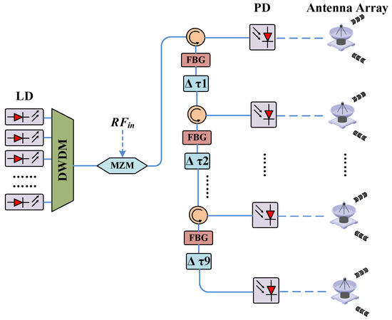
Figure 1.
The PAA application of the microwave photonic TTD system.
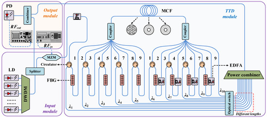
Figure 2.
A schematic diagram of the microwave photonic TTD system.

Table 1.
An explanation of the abbreviation in Figure 2.
There are two important devices in the whole MFBGs delay system, splitter and combiner, when we take the carrier compensation technology into account. The splitter separates a laser, as a beam of the compensating carrier, from the original laser combining the ten lasers, and takes it to an input port of the combiner. In the TTD module, another laser of the splitter is used effectively, because the CS-DSB improves the modulation sidebands compared to the double-sideband (DSB) modulation. Additionally, the following erbium-doped fiber amplifier (EDFA) amplifies the sidebands more than the central carriers under the CS-DSB, and the lack of the optical carrier power is compensated by the combiner. In principle, the illustrated microwave photonic TTD system presents a better ability to microsecond delay in comparison to the traditional TTD system based on the FBG. Figure 3a,b show the optical spectrum of the general delay system and proposed delay system before entering the PD, which carry out the DSB modulation and CS-DSB modulation separately; furthermore, one applies carrier compensation while the other doesn’t. Here, we ignore the higher-order sidebands (≥2) under the small-signal modulation condition. It is evidenced that our system can produce higher modulation sidebands, almost equivalent to the central optical carrier, when the CS-DSB modulation and carrier compensation are performed.
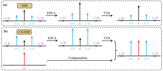
Figure 3.
The optical spectrum of the (a) general delay system and (b) proposed delay system before entering the PD.
3. Simulation Results
A simulation in accordance with Figure 2 was implemented through OptiSystem. The linewidth and power of the lasers are 5 MHz and 10 dBm, respectively. The wavelength spacing between the two lasers is set to 1.6 nm, which corresponds to two standard channel intervals of 0.8 nm. A sufficiently long wavelength spacing is necessary so that the MFBGs do not interfere with the adjacent channels when they reflect the light signals. In the settings, an MZM is adopted whose lower and upper ports have opposite electrical phases, and the MZM has the extinction ratio of 30 dB. In addition, the switching bias voltage and the bias voltage of upper arm are set to 6 V to carry out the CS-DSB modulation. The PD has a responsivity of 0.8 A/W that is consistent with reality. In the TTD module, the delay lines use time delayers instead of optical fibers to simplify the simulation, and the delay time is set to 10 μs.
The result of six-channel delay is shown in Figure 4. A rectangular monopulse signal is modulated on an RF carrier, which has the frequency of 20 GHz. The modulation monopulse signal is modulated again on six-channel optical carriers by the MZM, and then the original signal is densely copied to produce six pulse signals. Monitoring through a time window, we see that the pre-designed interval of 10 μs and total delay time of 50 μs are obtained. In order to explain the advantages of carrier compensation, a comparative simulation is completed on the two different schemes according to Figure 3. All setup conditions except the modulation format of the MZM remain unchanged to ensure the effectiveness of the comparison results. As can be seen from Figure 5, the optical power of the +1 order sideband enhances 18.7 dBm after the carrier compensation. It is beneficial to strengthen the beating intensity between the central optical carrier and sidebands, and the electrical spectrum has a power improvement of 5.2 dBm in Figure 5e. Similarly, the amplitude of the delay signals has also been increased by nearly an order of magnitude. Therefore, from the point of view of simulation, the proposed microwave photonic TTD system verifies improved delay launch capability by applying the carrier compensation and CS-DSB modulation.
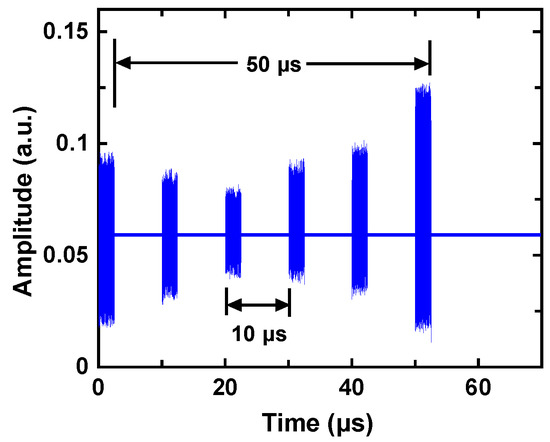
Figure 4.
The simulation result of six-channel TTD system.
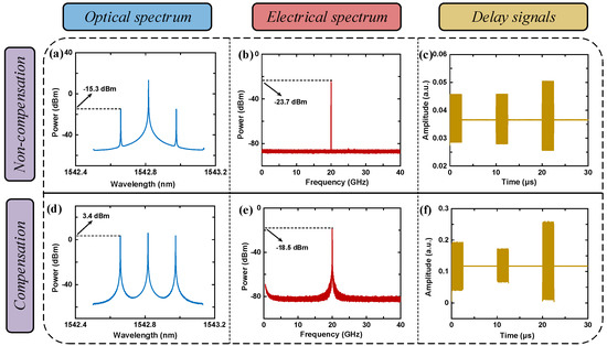
Figure 5.
The optical spectrum, Electrical spectrum and delay signals of (a–c) TTD system without carrier compensation and (d–f) compensation TTD system with carrier compensation.
4. Experimental Results
4.1. Experimental Setup
The experiment based on the setup of Figure 2 is carried out in Figure 6. The wavelength intervals and output optical power of all the LDs are set at 1.6 nm and 10 dBm, respectively, to satisfy the requirements of the link. The ten standard channels, whose wavelengths range from 1542.142 nm to 1556.555 nm, are selected for the DWDM. The commercial modulator (ixblue, MXAN-LN-20) is connected to the DWDM so that the optical carriers can be coupled to the MZM. The MZM has the half-wave voltage of 5 V and optical insertion loss of 3.5 dB, and the CS-DSB is finished by simply controlling the bias voltages of the modulator. The central reflection wavelength of the FBG should be matched with the laser and multiplexing channel; additionally, the reflection bandwidth of 0.35 nm is enough to ensure that both the optical carrier and sidebands are reflected. Except for the EDFA amplifying the sideband signals, four EDFAs are connected either behind the FBGs for the purpose of optical power compensation. The pump power and amplification gain of the single EDFA are 5 dBm and 25 dB, respectively, under the working current of 100 mA. Finally, the photoelectric conversion is completed using the PD, which has the responsivity of 0.8 A/W and the bandwidth of 18 GHz. In order to achieve adjustable delay, there are several optical fibers with different lengths after the optical switch; moreover, the insertion loss 2 dB and switching time 3 ms of the optical switch can meet the experimental demand.
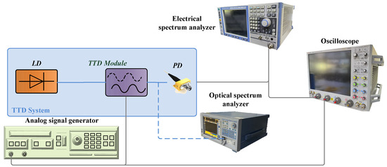
Figure 6.
Experiment setup of the TTD system test.
In the experiment, we need to balance the relationship between power budget and system performance. More optical power is not always better, as it is subject to the power limits of the MZM and PD. For the MZM, the maximum input optical power is 20 dBm; for the PD, the input saturated optical power is 13 dBm. So, a larger power budget is better without exceeding device power limits. This is conducive to improving the signal quality.
4.2. Optical Spectrum
First, the CS-DSB modulation of the proposed microwave photonic TTD system is analyzed in the optical domain. The benefits of the carrier compensation are evaluated using an optical spectrum analyzer (OSA, YOKOGAWA, AQ6370D). To observe the sidebands and carrier changes clearly, an analog signal generator (ASG, KEYSIGHT E8267D) outputs the RF signal of 20 GHz and 10 dBm. When the ten-channel optical carriers pass through the DWDM, MZM, EDFA, and TTD system in turn, the optical spectrum is shown in Figure 7. In the experimental link, two optical attenuators are set at the outputs of the channels λ5 and λ10, resulting in a 7.2 dB power difference between the channel λ10 and others. The purpose is to reduce optical power on the last two delay channels, λ5 and λ10; otherwise, the reflected signals in the rear orders will be amplified all the time until saturation. As shown in Figure 7b, the modulation +1 order sideband of the channel λ1 exhibits an optical power of −31.4 dBm; it obviously cannot support the follow-up photoelectric detection. Therefore, after the EDFA, the sideband power is up to a level greater than −20 dBm. It is observed that the power of the central carriers is also increased a lot, because the MZM has a relatively small extinction ratio (25 dB) and shows a not-very-strong suppression ability of optical carriers. Although the carrier suppression is not significant, the power of the sideband is still much improved compared with DSB. Figure 8 compares the two modulation schemes, and we can see that the strength of +1 order sideband signal improves 13.5 dB through EDFA. Because EDFA concentrates its amplification power on high-power optical signals, the magnification is transferred to the sideband under the CS-DSB. Therefore, a high-quality beat signal can be obtained with the compensated center carrier and high-power sideband. For the channel λ3, the reflection characteristic of the FBG is described in Figure 7e, and a side-mode suppression ratio of larger than 41.4 dB is sufficient to not affect the adjacent channels. With going through the TTD system, the optical signals to be beat have almost no power loss compared to Figure 7c, because the EDFAs provide full power compensation. More importantly, in Figure 7d, the sideband power is almost comparable to the central carrier, which benefits from the carrier compensation and CS-DSB modulation. It should be noted that the noise floor of the spectrum is not flat, which is caused by the non-flat EDFA gain.
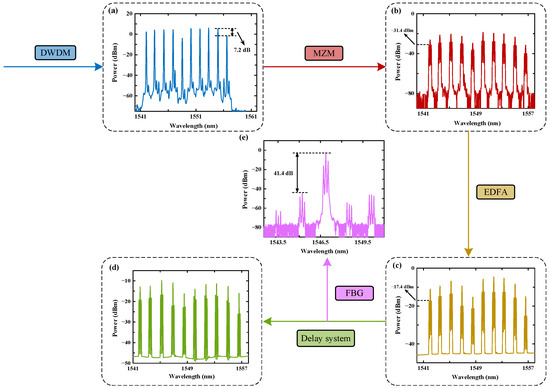
Figure 7.
The optical spectrum when the ten-channel optical carriers pass through the (a) DWDM, (b) MZM, (c) EDFA, and (d) TTD system. (e) The FBG reflection optical spectrum of the channel.
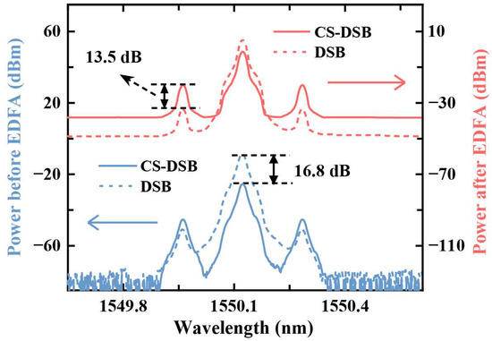
Figure 8.
Measured optical spectrum before and after EDFA.
4.3. Electrical Spectrum
The features of the electrical spectrum are demonstrated using an electrical spectrum analyzer (ESA, ROHDE&SCHWARZ). The measured output spectrum of the beating signals is described in Figure 9a where the RF carrier has the frequency of 6 GHz and power of 0 dBm. The output RF signal achieves the peak power of 4.45 dBm and has the spurious suppression of more than 60 dBc at 6 GHz. By comparing the RF power of output to input, the microwave photonic TTD system realizes a 3 dB gain instead of loss owing to the EDFAs.
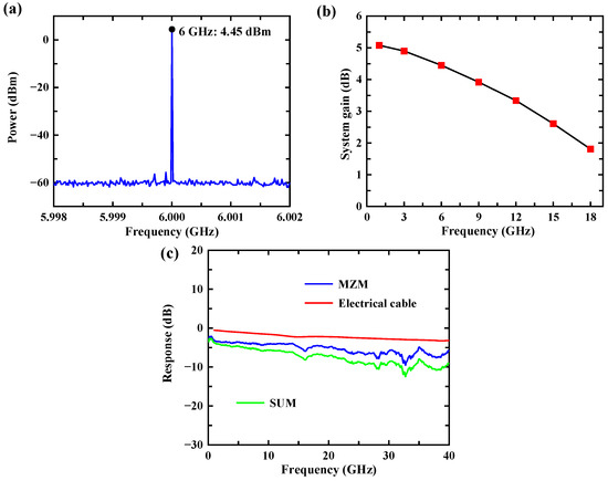
Figure 9.
(a) The measured output spectrum, (b) the system gain from 0.8 to 18 GHz, and (c) the measured power responses of electrical cable and MZM.
The system gain represents the power response of the proposed TTD system. The RF frequency is tuned from 0.8-18 GHz in order to measure the system gain shown in Figure 9b. Furthermore, the power of the input RF signal is fixed at 0 dBm, which is in the linear response region of the whole system. We can see that the system gain decreases with the increase in the RF frequency from Figure 9b. To further analyze the influencing factors of system gain, the power responses of the electrical cable and MZM are measured and illustrated in Figure 9c. According to the response curves, we find that the transmission responses of both drop at higher frequencies and microwave loss reaches 3.2 dB and 5.8 dB, respectively, at 40 GHz, which coincides with the downtrend of the system gain. To improve the flatness of system gain, the MZM with a better bandwidth curve or response equalization technique can be considered.
4.4. Time Domain Results
We set the transmitting RF frequency of the ASG as 6 GHz, the transmitting power as 10 dBm, and the ASG under pulse mode that has the pulse frequency 1 kHz and pulse width 3 μs; thus, periodic rectangular pulses modulated on the RF carrier are acquired. An oscilloscope (DSAZ594A, KEYSIGHT) gives measurement results shown in Figure 10 for the TTD system. In Figure 10a, the initial total delay time of ten replicate signals attains 90.103 μs, so the feasibility of the system in microsecond delay is verified experimentally. The performance of optical switching is also demonstrated by changing the length of the delay fiber, and the delay interval between the 3rd signal and the 10th signal is increased from 66.448 μs to 71.373 μs. In addition, the total delay changes to 92.514 μs. On the other hand, response time to the original signal must be considered, which is defined by the launch time from the original pulse to first copy. When testing the response time, a power divider is needed to separate half of the initial pulse, called the pulse in contrast, from the ASG. As can be seen from Figure 10b, the TTD system enjoys a response time of 172.74 ns. Therefore, the response speed in our system is sufficient for most practical applications of beamforming and radar detection.
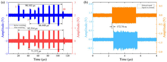
Figure 10.
(a) The total time domain results and (b) response time.
5. Discussion
It is noteworthy that the delay signals in Figure 10a exhibit a heterogeneity in amplitude, since strain perturbation on some FBGs can cause a shift of the central reflection wavelength leading to incomplete reflection. To solve the problem introduced by the heterogeneity, a variable optical attenuator (VOA) needs to be connected behind the optical switch, which attenuates each channel with unequal amplitude to maintain consistency of the amplitude.
In practice, the phase interference problem is of great importance, which is mainly reflected in three points: the influence of the phase during compensation, the laser coherence during the propagation, and the fiber dispersion. The coherence length calculation formula is given by
where nm is the refractive index of the material, λ0 is the central wavelength of the laser, and Δλ is the full-width at half-maximum (FWHM) in wavelength [22]. We found that the coherence length of the laser is about 200 m. To achieve a coherence length of 20 km, the linewidth of the laser should be 10 KHz, but this requires a high level of laser, which will lead to increased costs. We assume that the angular frequencies of the transmission sideband and the compensating carrier are ω1 and ω2, respectively; the PD beating formula is given by
where R is the responsiveness of PD, E1 and E2 are the light field intensity of the two beams, and φ1 and φ2 are the phase of the two beams. That means as long as we make sure the phases of the two beams are related, the phase of the electrical signal is determined. Furthermore, the optical fibers and discrete devices may have phase jitter. This can be resolved using a piezoelectric (PZT) PM fiber stretcher, which takes advantage of the feedback loop to control the phase of two beams of light [23]. On the other hand, since the compensated optical carrier power is much higher than the transmitted carrier power, generally much higher than 3 dB, the power cancellation due to phase difference is small enough so that the compensation effect on the transmitted optical carrier is still strong. The use of the same one laser ensures that the phase of the optical signal is correlated before and after the delay. The final factor that has a great influence on the phase is fiber dispersion, when we think about a very long optical fiber. Fiber dispersion creates a time delay Δτ between adjacent signals. That will increase phase difference Δφ = 2πfΔτ, which limits the application of PAA. To solve the problem introduced by dispersion, dispersion compensation techniques, such as Bragg grating dispersion compensation [24], chirp compensation [25], and dispersion compensation fiber (DCF) [26], are necessary in the application.
The temperature stability of the whole link is mainly determined by the laser. Typically, a 1 °C increase in temperature results in a wavelength shift of 0.1 nm. Thus, the temperature control circuit is very important to stabilize the wavelength. It uses thermistors to convert the temperature into electrical signals and sends them to a thermo-electric cooler (TEC) through a proportion–integration–differentiation (PID) control circuit, which then allows TEC to control the temperature. After the analysis of temperature stability, our TTD system can operate at 25 °C ± 20 °C.
6. Conclusions
In this paper, a novel microwave photonic TTD system using carrier compensation technology is proposed and experimentally demonstrated. The compensation carrier is combined with the time-delayed optical signals to be detected. Meanwhile, sideband signals are amplified effectively thanks to the CS-DSB modulation. So, the power of both the central optical carriers and sidebands is guaranteed, which produces a better beat-frequency result than the TTD system without carrier compensation. The simulation results confirm that the signal amplitude has an order of magnitude improvement due to the compensation. With employing the delay fibers based on MFBGs, the experimental delay and response time reach 90.103 μs and 172.74 ns. The proposed technique can find applications in time-delay beamforming of PAAs.
Author Contributions
Conceptualization, Y.Z. and C.W.; hardware, Y.Z., C.W. and Z.Z.; validation, W.Z. and Z.Z.; writing—original draft preparation, Y.Z. and C.W.; writing—review and editing, W.Z. and J.L.; project administration, J.L., C.W. and Y.Z. contributed equally to this work. All authors have read and agreed to the published version of the manuscript.
Funding
This work is supported by the National Natural Science Foundation of China (61727815).
Informed Consent Statement
Not applicable.
Data Availability Statement
No new data were created or analyzed in this study. Data sharing is not applicable to this article.
Acknowledgments
The authors are grateful to the State Key Laboratory on Integrated Optoelectronics, Institute of Semiconductors, Chinese Academy of Sciences and School of Integrated Circuits, University of Chinese Academy of Sciences.
Conflicts of Interest
The funders had no role in the design of the study; in the collection, analyses, or interpretation of data; in the writing of the manuscript, or in the decision to publish the results.
References
- Longbrake, M. True Time-Delay Beamsteering for Radar. In Proceedings of the 2012 IEEE National Aerospace and Electronics Conference (NAECON), Dayton, OH, USA, 25–27 July 2012; IEEE: Manhattan, NY, USA, 2012; pp. 246–249. [Google Scholar]
- Capmany, J.; Novak, D. Microwave Photonics Combines Two Worlds. Nat. Photon. 2007, 1, 319–330. [Google Scholar] [CrossRef]
- Rotman, R.; Tur, M.; Yaron, L. True Time Delay in Phased Arrays. Proc. IEEE 2016, 104, 504–518. [Google Scholar] [CrossRef]
- Jung, B.-M.; Shin, J.-D.; Kim, B.-G. Optical True Time-Delay for Two-Dimensional X-Band Phased Array Antennas. IEEE Photon. Technol. Lett. 2007, 19, 877–879. [Google Scholar] [CrossRef]
- Wang, J.; Hou, P.; Cai, H.; Sun, J.; Wang, S.; Wang, L.; Yang, F. Continuous Angle Steering of an Optically- Controlled Phased Array Antenna Based on Differential True Time Delay Constituted by Micro-Optical Components. Opt. Express 2015, 23, 9432. [Google Scholar] [CrossRef] [PubMed]
- Ding, Z.; Yang, F.; Cai, H.; Weng, Y.; Wang, M.; Wang, D. Photonic Radio Frequency Memory with Controlled Doppler Frequency Shift. In Proceedings of the 2019 International Topical Meeting on Microwave Photonics (MWP), Ottawa, ON, Canada, 7–10 October 2019; IEEE: Manhattan, NY, USA, 2019; pp. 1–3. [Google Scholar]
- Nguyen, T.A.; Chan, E.H.W.; Minasian, R.A. Photonic Radio Frequency Memory Using Frequency Shifting Recirculating Delay Line Structure. J. Light. Technol. 2014, 32, 99–106. [Google Scholar] [CrossRef]
- Qi, K.; Zhang, Y.; Wu, Y.; Li, H.; Yuan, P. Tunable and Flat Optical Delay Line Based on Double Rings Resonators. In Quantum and Nonlinear Optics IV, Proceedings of the SPIE/COS Photonics Asia, Beijing, China, 3 November 2016; Gong, Q., Guo, G.-C., Ham, B.S., Eds.; SPIE: Bellingham, WA, USA, 2016; p. 1002916. [Google Scholar]
- Khurgin, J.B.; Morton, P.A. Tunable Wideband Optical Delay Line Based on Balanced Coupled Resonator Structures. Opt. Lett. 2009, 34, 2655. [Google Scholar] [CrossRef] [PubMed]
- Brunetti, G.; Conteduca, D.; Dell’Olio, F.; Ciminelli, C.; Armenise, M.N. Design of an Ultra-Compact Graphene-Based Integrated Microphotonic Tunable Delay Line. Opt. Express 2018, 26, 4593. [Google Scholar] [CrossRef] [PubMed]
- Zhang, Q.; Ji, J.; Cheng, Q.; Duan, Y.; Zang, J.; Yang, J.; Yu, H.; Zhang, X. Two-Dimensional Phased-Array Receiver Based on Integrated Silicon True Time Delay Lines. IEEE Trans. Microw. Theory Tech. 2022, 1–11. [Google Scholar] [CrossRef]
- Moreira, R.L.; Garcia, J.; Li, W.; Bauters, J.; Barton, J.S.; Heck, M.J.R.; Bowers, J.E.; Blumenthal, D.J. Integrated Ultra-Low-Loss 4-Bit Tunable Delay for Broadband Phased Array Antenna Applications. IEEE Photon. Technol. Lett. 2013, 25, 1165–1168. [Google Scholar] [CrossRef]
- Sancho, J.; Bourderionnet, J.; Lloret, J.; Combrié, S.; Gasulla, I.; Xavier, S.; Sales, S.; Colman, P.; Lehoucq, G.; Dolfi, D.; et al. Integrable Microwave Filter Based on a Photonic Crystal Delay Line. Nat. Commun. 2012, 3, 1075. [Google Scholar] [CrossRef] [PubMed]
- Zhang, W.; Yao, J. A Fully Reconfigurable Waveguide Bragg Grating for Programmable Photonic Signal Processing. Nat. Commun. 2018, 9, 1396. [Google Scholar] [CrossRef] [PubMed]
- Liu, J.; Cheng, T.H.; Yeo, Y.K.; Wang, Y.; Xue, L.; Zhu, N.; Xu, Z.; Wang, D. All-Optical Continuously Tunable Delay with a High Linear-Chirp-Rate Fiber Bragg Grating Based on Four-Wave Mixing in a Highly-Nonlinear Photonic Crystal Fiber. Opt. Commun. 2009, 282, 4366–4369. [Google Scholar] [CrossRef]
- Cheng, T.-H.; Liu, J.; Yeo, Y.; Wang, Y.; Xu, Z.; Wang, D. Hi-Fi All-Optical Continuously Tunable Delay with a High Linear-Chirp-Rate Fiber Bragg Grating Based on Four-Wave Mixing in a Highly-Nonlinear Photonic Crystal Fiber. In Proceedings of the Optical Fiber Communication Conference and National Fiber Optic Engineers Conference, San Diego, CA, USA, 22–26 March 2009; p. JWA31. [Google Scholar]
- Pisco, M.; Campopiano, S.; Cutolo, A.; Cusano, A. Continuously Variable Optical Delay Line Based on a Chirped Fiber Bragg Grating. IEEE Photon. Technol. Lett. 2006, 18, 2551–2553. [Google Scholar] [CrossRef]
- Zhao, J.; Ding, Z.; Yang, F.; Cai, H. Configurable Photonic True-Time Delay Line Based on Cascaded Linearly Chirped Fiber Bragg Grating. In Proceedings of the 2018 International Topical Meeting on Microwave Photonics (MWP), Toulouse, France, 22–25 October 2018; IEEE: Manhattan, NY, USA, 2018; pp. 1–4. [Google Scholar]
- Italia, V.; Pisco, M.; Campopiano, S.; Cusano, A.; Cutolo, A. Tunable Optical True Time Delay Line Based on Fiber Bragg Grating. In Proceedings of the 2005 IEEE/LEOS Workshop on Fibres and Optical Passive Components, Palermo, Italy, 22–24 June 2005; IEEE: Manhattan, NY, USA, 2005; pp. 345–348. [Google Scholar]
- Ball, G.A.; Glenn, W.H.; Morey, W.W. Programmable Fiber Optic Delay Line. IEEE Photon. Technol. Lett. 1994, 6, 741–743. [Google Scholar] [CrossRef]
- Molony, A.; Zhang, L.; Williams, J.A.R.; Bennion, I.; Edge, C.; Fells, J. Fiber Bragg-Grating True Time-Delay Systems: Discrete-Grating Array 3-b Delay Lines and Chirped-Grating 6-b Delay Lines. IEEE Trans. Microw. Theory Tech. 1997, 45, 1527–1530. [Google Scholar] [CrossRef]
- Zhang, C.; Liao, P.; Burgoyne, B.; Kim, Y.; Trepanier, F.; Villeneuve, A.; Liboiron-Ladouceur, O. Low-Cost Dispersion-Tuned Active Harmonic Mode-Locked Laser With a 3-Cm Coherence Length. IEEE J. Select. Top. Quantum Electron. 2014, 20, 399–405. [Google Scholar] [CrossRef]
- Morton, P.A.; Khurgin, J.B.; Morton, M.J. All-Optical Linearized Mach-Zehnder Modulator. Opt. Express 2021, 29, 37302. [Google Scholar] [CrossRef] [PubMed]
- Inui, T.; Komukai, T.; Nakazawa, M.; Suzuki, K.; Tamura, K.R.; Uchiyama, K.; Morioka, T. Adaptive Dispersion Slope Equalizer Using a Nonlinearly Chirped Fiber Bragg Grating Pair with a Novel Dispersion Detection Technique. IEEE Photon. Technol. Lett. 2002, 14, 549–551. [Google Scholar] [CrossRef]
- Lanne, S.; Penninckx, D.; Thiery, J.-P.; Hamaide, J.-P. Impact of Chirping on Polarization-Mode Dispersion Compensated Systems. IEEE Photon. Technol. Lett. 2000, 12, 1492–1494. [Google Scholar] [CrossRef]
- Dong, B.; Wei, L.; Zhou, D.P. Coupling Between the Small-Core-Diameter Dispersion Compensation Fiber and Single-Mode Fiber and Its Applications in Fiber Lasers. J. Light. Technol. 2010, 28, 1363–1367. [Google Scholar] [CrossRef]


Disclaimer/Publisher’s Note: The statements, opinions and data contained in all publications are solely those of the individual author(s) and contributor(s) and not of MDPI and/or the editor(s). MDPI and/or the editor(s) disclaim responsibility for any injury to people or property resulting from any ideas, methods, instructions or products referred to in the content. |
© 2022 by the authors. Licensee MDPI, Basel, Switzerland. This article is an open access article distributed under the terms and conditions of the Creative Commons Attribution (CC BY) license (https://creativecommons.org/licenses/by/4.0/).