Abstract
We demonstrate a fourth-order Vernier serious-coupled microring resonator (MRR) filter based on the InGaAs/InAlAs five-layer asymmetric coupled quantum-well (FACQW) waveguide. As the tuning of the main resonance wavelength is driven by the electrorefractive index change in the FACQW layer caused by the quantum-confined Stark effect (QCSE), the MRR filter has lower tuning power consumption and high-speed operation. The free spectral range (FSR) of the MRR filter is extended to 9.4 nm. The main resonant peak is discretely tuned within one FSR, leading to an increase in the wavelength channel.
1. Introduction
With the growing demand for data bandwidth, traditional electronic integrated circuits are facing the problem of high-power consumption and long latency, which poses a great challenge to the development of electronic integrated circuits. Photonic integrated circuits have emerged as a promising platform to solve these problems due to their low latency, high integration, and low power consumption. A microring resonator (MRR) is one of the key components for realizing optical large-scale integrated circuits because of its compact structure and flexible function configuration.
MRRs are used in many optical devices, such as dispersion compensators [1], lasers [2,3], optical modulators [4,5], optical switches [6,7], delay lines [8,9], isolators [10,11], optical memories [12,13], and sensors [14,15]. MRR filters are a viable device in the wavelength division multiplexing (WDM) system to extract a wavelength over a broad spectral range. To date, various MRR filters have been proposed and demonstrated based on SiN [16], lithium niobate [17], and polymers [18]. Furthermore, silicon-based MRR filters have attracted the attention of many researchers because of their low propagation, high-index contrast, and excellent filtering features. Liu et al. have demonstrated a low-loss add-drop MRR filter with an FSR of 93 nm using bent asymmetrical direction couplers [19]. Hu et al. demonstrated a thermally tunable Si third-order MRR filter with a tuning efficiency of 48.4 mV/nm [20]. Liu et al. employed the opto-mechanical effect in MRR tuning, and the wavelength tuning efficiency of the MRR filter reached 0.043 nm/mW [21]. However, most of the MRR filters are mainly derived from the thermo-optic (TO) effect to achieve wavelength tuning. Although the TO effect-driven MRR wavelengths have a wide range and a stable optical characteristic, it is challenging to operate at high speeds with lower power consumption. In addition, Si-based devices cannot be seamlessly integrated with semiconductor active devices, such as lasers composed of III–V semiconductors.
To solve the above problems, our laboratory has developed the InGaAs/InAlAs-based five-layer asymmetric coupled quantum well (FACQW) structure as the waveguide for optical devices [22]. The electrorefractive index change in the FACQW waveguide is achieved using the quantum-confined Stark effect (QCSE), which contributes to the realization of optical devices with high-speed operation and low tuning power consumption. Various optical devices based on the FACQW structure have been proposed [23,24,25]. Furthermore, the hitless wavelength-selective switch, namely MRR filters, with fourth-order MRR using FACQW waveguides is reported [26], which exhibits a microwatt level tuning power consumption and an operation speed of 2 ns. This means that optical devices based on FACQW also have low tuning power consumption and high-speed operation. However, the bending loss of the FACQW-based waveguide is so large that the FACQW-based MRR filter cannot increase the FSR by reducing the round-trip length of the MRR, like Si-based MRR filters. The FSR and the wavelength tuning range of the MRR filter in [26] are approximately 1.9 nm and 0.7 nm, respectively. Nevertheless, a larger FSR is required to maximize the number of channels that can be multiplexed. In the design of MRR filters, the Vernier effect is often adopted to extend the FSR using the MRRs with different round-trip lengths, thereby increasing the number of channels in WDM systems [27,28]. To date, the Vernier MRR filter based on the multiple-quantum-well (FACQW) waveguides has not been demonstrated.
In this study, we experimentally demonstrate a fourth-order Vernier series-coupled MRR filter based on FACQW waveguides. Its FSR is extended to 9.4 nm. Additionally, applying voltages in the vertical direction of MRRs enables the resonance wavelength to be discretely tuned with a step of 1.8 nm or 1.5 nm within one FSR due to the Vernier effect.
2. Working Principle and Transfer function
Generally, the Vernier MRR filters are composed of two MRRs with different round-trip lengths and two or three parallel waveguides. Figure 1a,b show the working principle of the Vernier effect and the spectral response schematic in the drop port, respectively. The FSR of MRRs is inversely proportional to the round-trip length of the MRR. The FSR1 and FSR2 in Figure 1a correspond to the MRR1 and MRR2, respectively. The main resonance peaks, the black dashed line in Figure 1a, will appear when the resonance peaks from MRR1 to MRR2 are aligned, as illustrated in Figure 1a.
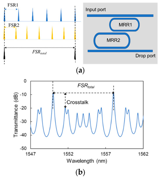
Figure 1.
(a) Working principle of the Vernier effect and second-order Vernier MRR filter structure. (b) The theoretical spectral response in the drop port.
The main resonance peak will be red-shifted in the steps of the FSR of the untuned MRR. However, to reduce the bending loss of the FACQW-based waveguide, the round-trip length of the FACQW-based MRR filter is several hundred micrometers, and the wavelength tuning range is less than 1 nm [23]. When the channel spacing in WDM systems is 0.8 nm, only one wavelength channel can be utilized. Thus, it is necessary to reduce the difference between the two FSRs to extend the tuning range of the main resonance peak with a tuning range of 1 nm. Nevertheless, the small difference between FSR1 and FSR2 will cause the resonance peaks next to the main resonance peak to partially overlap to form a strong resonance peak, resulting in serious crosstalk (i.e., small interstitial peak suppression). The crosstalk can be suppressed using high-order series-coupled MRRs [29].
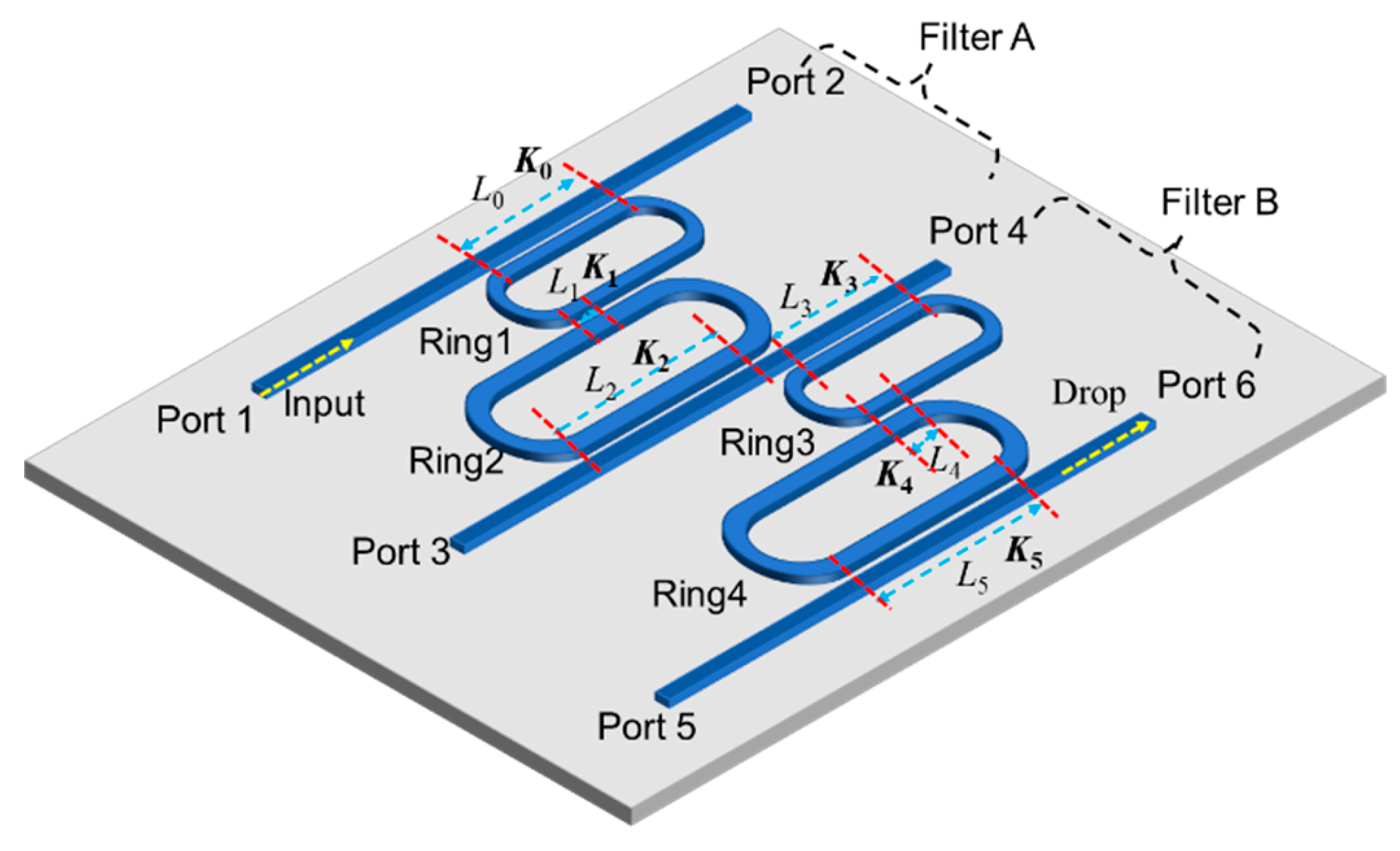
A fourth-order Vernier MRR filter is proposed in this study, as illustrated in Figure 2. A busline is introduced between Rings 2 and 3. It can be regarded as a combination of two MRR filters, Rings 1 and 2—which are considered Filter A—and Rings 3 and 4 as Filter B. This structure can precisely detect the MRRs that need to be tuned for the manufacturing error that causes the resonance peaks of MRRs to not be aligned by measuring the response spectra of Filter A and Filter B. In addition, the structure can also be used to confirm whether the Vernier effect exists by analyzing the spectra of Filter A and Filter B [28]. The light signal is input from Port 1, and the spectral response of the fourth-order Vernier MRR filter will be measured at Port 6.

Figure 2.
Schematic of the fourth-order Vernier MRR filter and its design parameters. L0 to L5 are the coupling lengths of the couplers.
The transfer function of the fourth-order Vernier MRR filter is basically similar to the transfer function of fourth-order MRR filters with the same round-trip lengths of MRRs [26,30]. The difference is that there is a busline between Rings 2 and 3 in the above structure, so additional transfer matrixes, C3 and C4, are added in the derivation of the transfer function. The drop port transfer of the Vernier fourth-order MRR filter can be determined using
where
where TA, RD, TI, and RT are the field amplitudes at Ports 2 5, 6, 1, and 2, respectively. Cn is the transfer matrix for the N-th coupler, corresponding to the area of L0 to L5 in Figure 2. The symbol ηn is the field amplitude transmission in a coupler region, and Kn and tn are the power coupling efficiency and power transmission at the n-th coupler, respectively. β and an are the propagation constant and the power transmittance in the MRR, respectively. The transfer function of the proposed MRR filter is equal to RD/TI.
3. Fourth-Order Vernier MRR Filter Design and Fabrication
3.1. MRR Filter Design
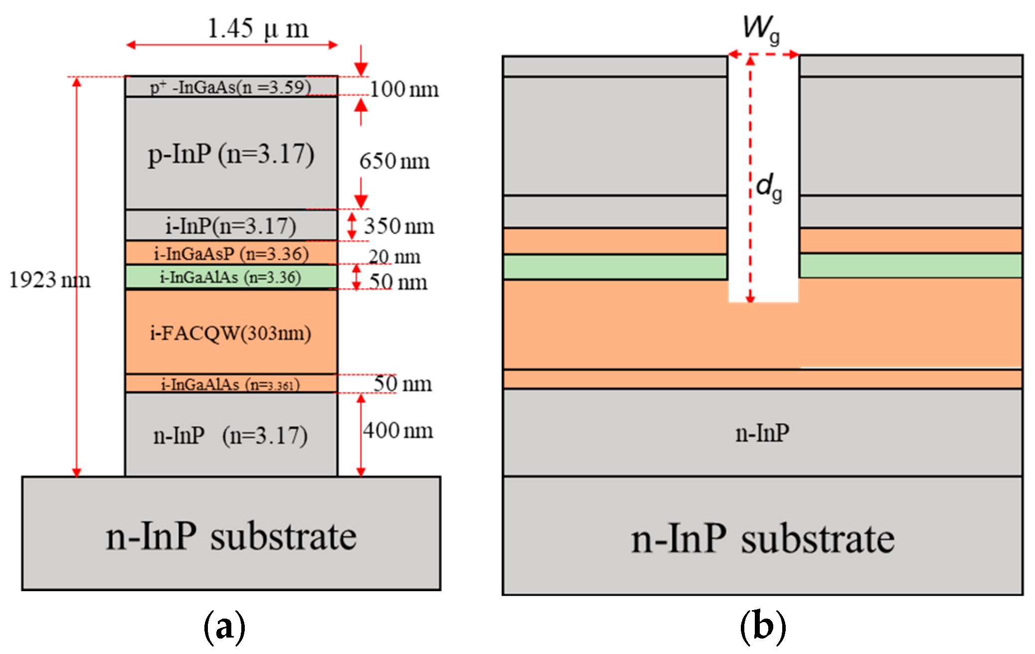
A schematic cross-section of the FACQW-based waveguide is shown in Figure 3a. The waveguide structure is the same as the second-order and fourth-order wavelength-selective switches reported by our research group [23,26]. The waveguide consists of a core layer with 12 periods of InGaAs/InAlAs (i-FACQW in Figure 3a), 50 nm of InAlGaAs, and 20 nm of i-InGaAsP separate confinement heterostructure layers, and a p/n-doped InP cladding layer. The refractive index and thickness of every layer in the waveguide are labeled in Figure 3a. The waveguide is surrounded by benzoncyclobutene (BCB) (refractive index is 1.543 at a wavelength of 1550 nm). The group index of the FACQW waveguide is 3.8. Figure 3b shows the schematic cross-sectional view of the coupling region. The width and depth of the groove in the coupling region are 300 nm and 1.27 μm, respectively. The amplitude transmission for the coupler is 0.96.
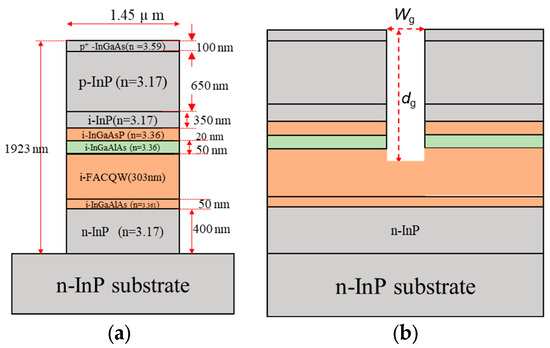
Figure 3.
Schematic cross-sectional views of (a) waveguide and (b) coupling regions.
The structure of the fourth-order Vernier MRR filter is shown in Figure 2, where the round-trip lengths of Rings 1 and 2, l1 and l2, are equal to those of Rings 3 and 4, l3 and l4, respectively. The FSRs of Rings 1 and 3 correspond to FSR1, and the FSRs of Rings 2 and 4 correspond to FSR2. The extended FSR, FSRtotal, is related to the FSR of Rings 1 and 2 using [28,31]
where m1 and m2 are co-prime integers. The round-trip lengths of the MRRs are determined using
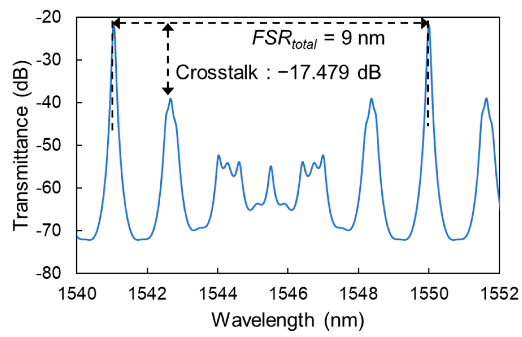
The ratio of m2 to m1 in this study is set at 5 to 6, and the FSRtotal is 9 nm. The round-trip lengths of Rings 1 and 3 are 351.19 μm, which corresponds to the FSR1 of 1.8 nm, and the round-trip lengths of Rings 2 and 4 are 421.36 μm with the FSR2 of 1.5 nm. The designed parameters of the proposed fourth-order Vernier MRR filter are summarized in Table 1. The calculated spectral response of the MRR filter is shown in Figure 4, which exhibits an extended FSRtotal of 9 nm. The difference between the intensity of the main resonance peak and the second-highest resonance peak within the FSR is defined as the crosstalk. The crosstalk of the designed MRR filter is −17.479 dB.

Table 1.
Designed parameters of fourth-order Vernier MRR filter.
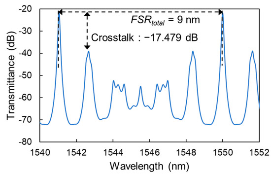
Figure 4.
Calculated spectral response of the fourth-order Vernier MRR filter.
3.2. Fabrication
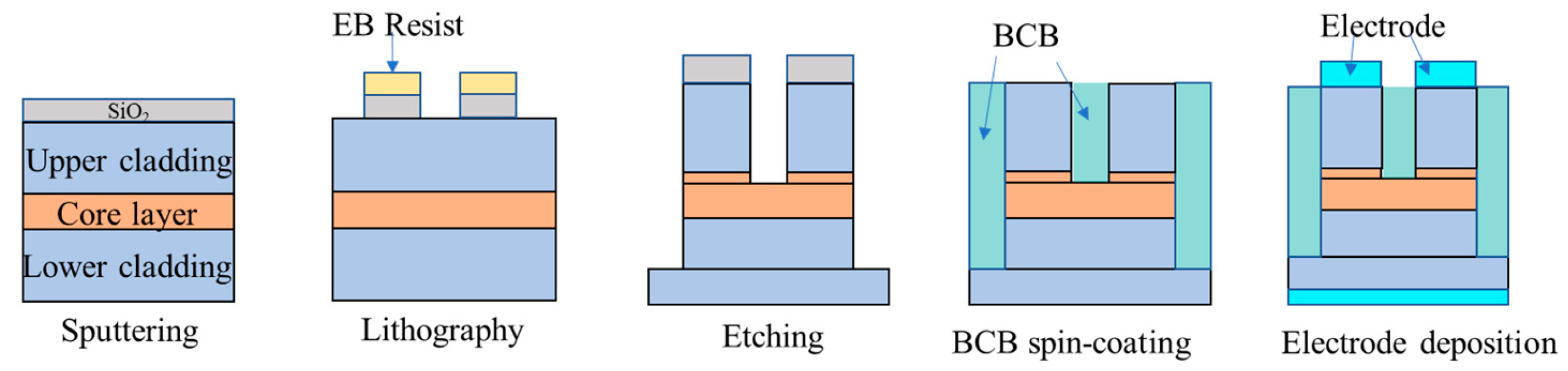
A 2-inch FACQW wafer is fabricated via metal-organic chemical vapor deposition (MOCVD). The wafer will be cut into a chip with a size of 1 × 1 cm2. Since the height of the designed waveguide is approximately 1.923 μm, it takes 4 min to form the waveguides in the process of etching. When Electron Beam (EB) resist is used directly as the mask layer for waveguides, the EB resist will be completely etched, which will result in the waveguide height not reaching 1.923 μm. Because SiO2 has a high etch selectivity ratio in InP etching, SiO2 is adopted as the mask layer for waveguides and grooves forming in this experiment. The main fabrication process is shown in Figure 5. Then, the resist required for exposure is spin-coated on the FACQW wafer, and the wafer is exposed via electron-beam lithography (Advantest F7000, ADVANTEST, Tokyo, Japan). After development, the pattern of the designed MRR filter is transferred to the resist. The remaining resist is used as a mask layer, and the wafer is etched using inductively coupled plasma reactive ion etching (ICP-RIE, Oxford ICP 180, Oxford Instruments, Oxfordshire, England) to form the waveguide and groove. Subsequently, BCB is filled around the waveguide, and metal electrodes are deposited on the top of the MRRs and the bottom of the chip.
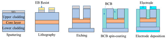
Figure 5.
Schematic of fabrication for the coupling area between MRRs.
There is a slight difference from the previous process [26]. The previous process utilized lithography and etching twice to form the waveguide and groove. Insufficient precision in the alignment exposure will easily lead to waveguide asymmetry on both sides of the groove and a lack of groove formation at one end of the coupling region. It will result in the upper cladding layers at both ends of the groove not being completely separated, thus preventing individual tuning of the MRRs. Therefore, the micro-loading effect in etching is used to simultaneously form waveguides and groves by once etching in this experiment. The benefit of using this method is that the upper cladding on both sides of the groove can be easily separated for individual tuning of the MRRs.
The scanning electron microscopy image of the cross-section of the coupler and the fabricated fourth-order MRR filter are shown in Figure 6. It can be seen from Figure 6a that the widths of the waveguide on both sides of the groove are almost the same. Due to the narrow etching area in the coupler, the etching plasma is not uniformly distributed, so the groove shows a V-shape. However, the depth of the groove reaches the core layer so that the upper cladding layers are completely separated, which enables MRRs to be tuned individually. Figure 7 shows the I-V characteristics when a reverse bias is performed in the vertical direction of the MRR. The reverse bias is controlled in the range of 0 V to −15 V to prevent high voltage breaking through the core layer. The current is less than 10 μA, so the tuning power consumption of a single FACQW-based MRR is less than 150 μW.
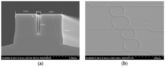
Figure 6.
Scanning electron microscopy image of (a) cross-section coupler and (b) proposed MRR filter.
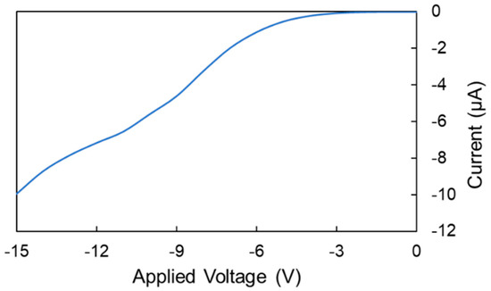
Figure 7.
I–V characteristic of the FACQW-based waveguide.
4. Result and Discussion
4.1. MRR Filter Characteristic
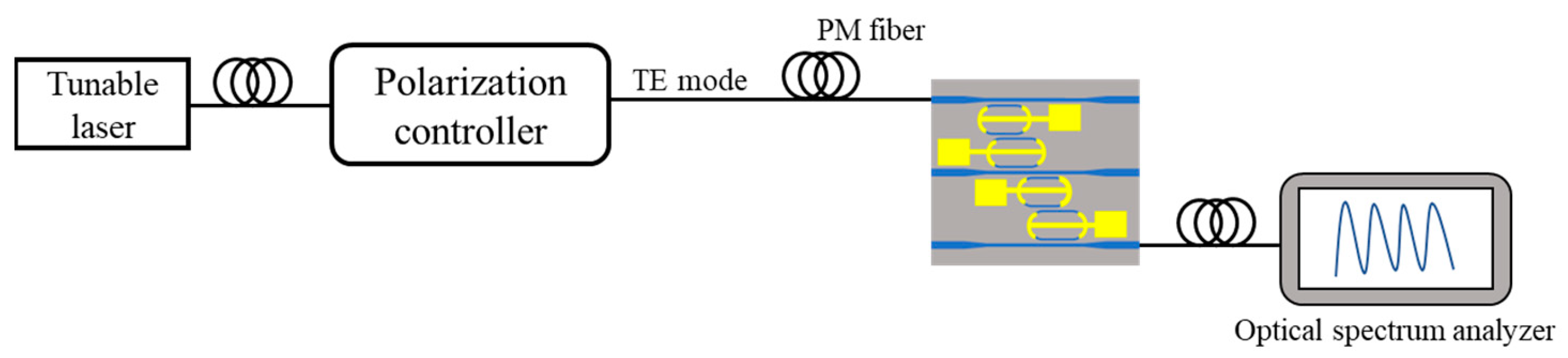
The equipment used in the measurement is an Agilent 816A tunable laser (Agilent, Santa Clara, CA, USA), a THORLABS PAT9000B polarization analyzer, and an Agilent 86082A spectrum analyzer. In the measurement setup, the lightwave signal with TE mode and an optical power output of 1 mW from the tunable laser is input to the MRR filter through the polarization controller (PM). The lightwave through the MRR filter is coupled to the optical fiber and then input to the spectrum analyzer, as shown in Figure 8. The entire chip is placed on a copper pedestal. Gold electrodes are deposited on the top of MRRs, as shown in Figure 8. Probes are used to contact the four electrode pads of the MRRs and form four sets of circuit loops with the copper pedestal to achieve MRR individual tuning. In addition, the diameter of the optical fiber spot is 9 µm, and the width of the waveguide is approximately 1.923 µm. Direct coupling between optical fibers and the waveguides will lead to mode mismatch, resulting in greater coupling loss. Therefore, tapers are used on the chip to reduce the coupling loss between optical fibers and the waveguides. A vertical electric field is applied to the waveguide through the top and bottom electrodes (Yellow part in Figure 8). Due to the application of an electric field, the refractive index of the waveguide will be changed to achieve tuning of the resonance peaks.
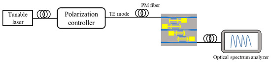
Figure 8.
Measurement setup schematic of MRR filter spectral response.
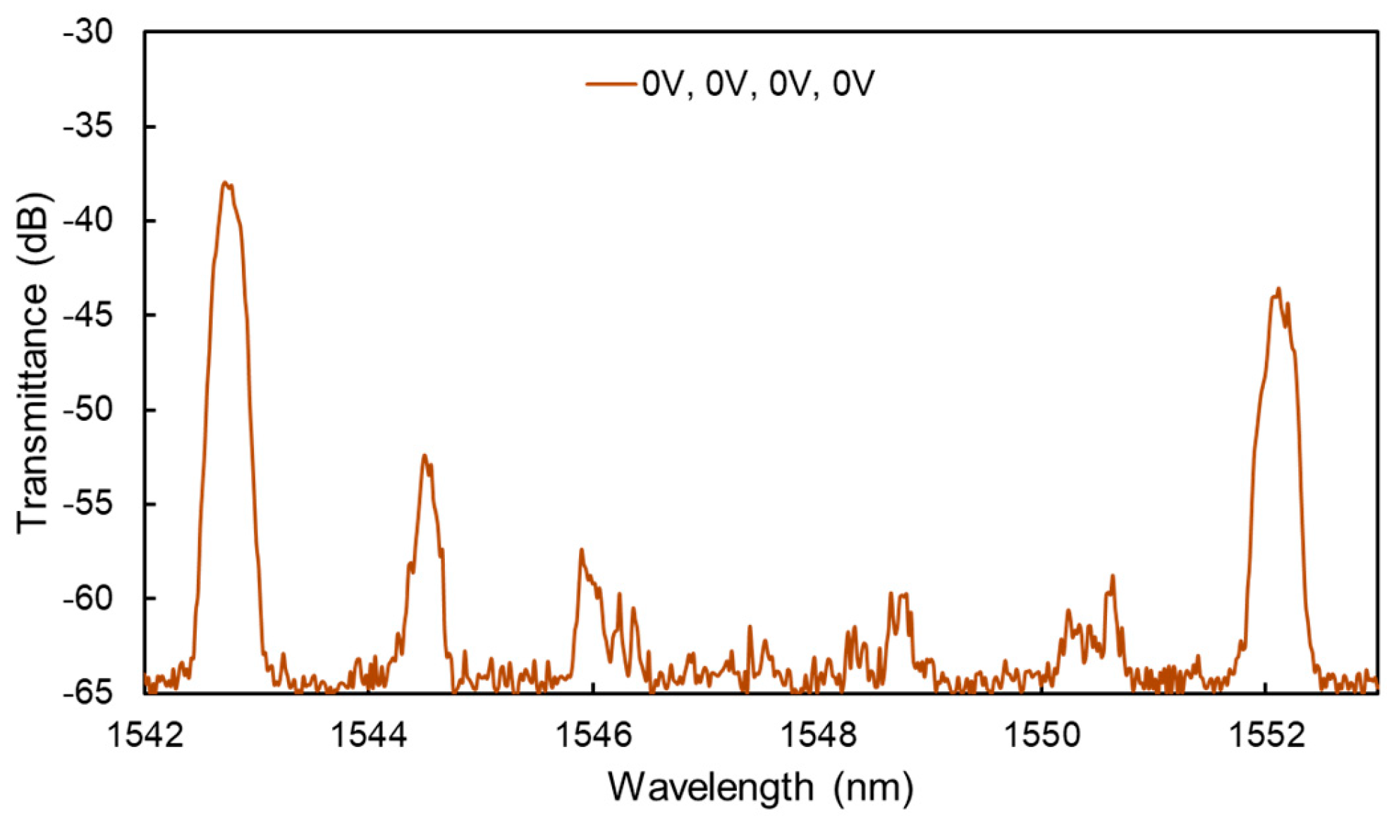
Figure 9 shows the measured drop-port spectral response of the proposed fourth-order Vernier MRR filter without reverse bias.

Figure 9.
Experimental drop-port spectral response of fourth-order Vernier MRR filter without reverse bias.
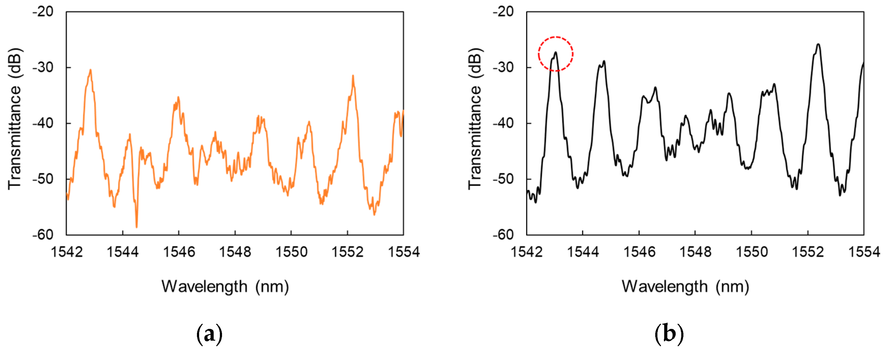
Two main resonance peaks appear in Figure 9, but there is a 5.619 dB difference in their intensities. It depicts that the resonance peaks are fully aligned and the MRRs need to be tuned. To find exactly the MRRs that need to be tuned, the spectral responses of Filter A (Input Port 1 and Output Port 4) and Filter B (Input Port 5 and Output Port 4) are measured. It can be seen from Figure 10a that there are two obvious main resonance peaks at the wavelengths of 1542.8 nm and 1552.2 nm. The main resonance peak is marked with a red dashed circle in Figure 10b, and the secondary resonance peak (next to the main resonance peak) has a larger crosstalk of −1.563 dB. Thus, Ring 3 or Ring 4 needs to be tuned to suppress the crosstalk. Figure 11 shows the spectral response of Filter B with −3 V applied to Ring 3, and the crosstalk is suppressed to −6.123 dB.
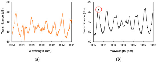
Figure 10.
Measured spectral response of (a) filter A and (b) filter B.
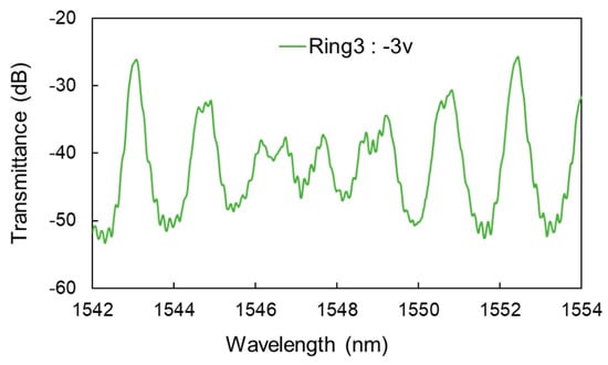
Figure 11.
Measured spectral response of filter B when −3 V is applied to ring 3.
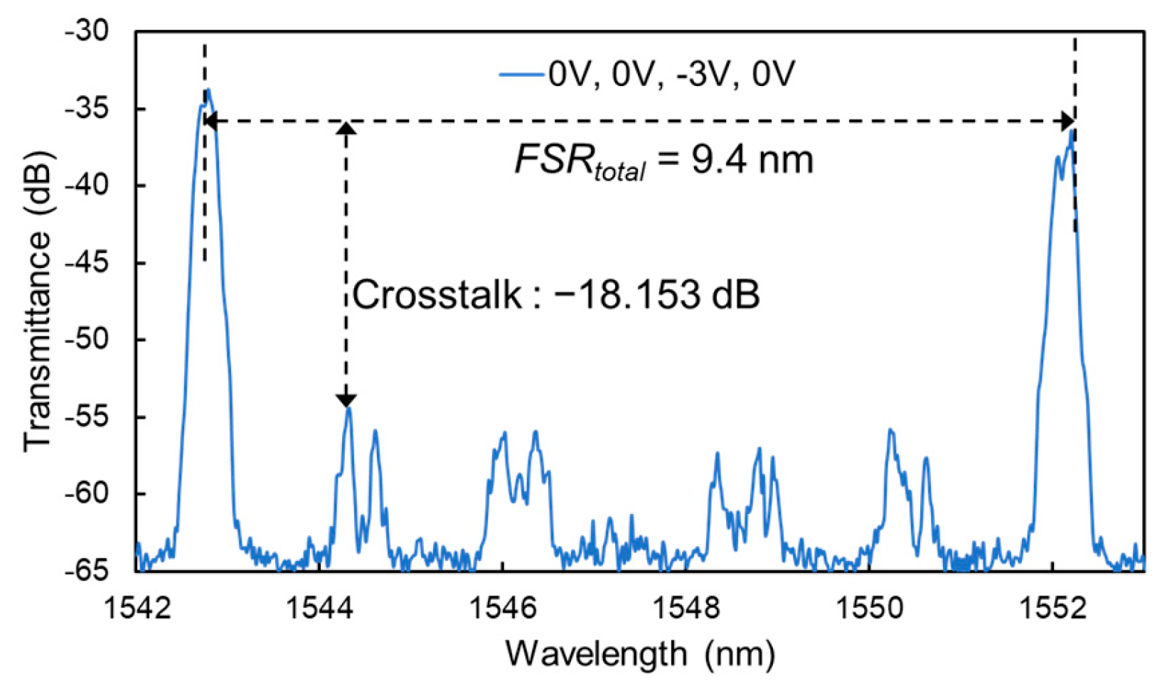
Figure 12 shows the measured drop port spectral response of the fourth-order Vernier MRR filter (light input from Port 1 and output from Port 6) when a voltage of −3 V is applied to Ring 3. The extended FSR, FSRtotal, is 9.4 nm, and the crosstalk is −18.153 dB, as illustrated in Figure 12. Manufacturing errors led to deviations between the actual round-trip lengths of the MRRs and the designed round-trip lengths. The ratio is not equal to 5 to 6, resulting in the resonance peaks of MRRs not being perfectly aligned. It causes a splitting of the main resonance peak on the right side in Figure 12, and the FSRtotal of 9.4 nm is slightly larger than the designed FSR of 9 nm. The total insertion losses for the drop port are 33.719 dB. The Q factor at the wavelength of 1542.8 nm is 8571. The fiber-to-fiber insertion loss in the process of optical performance measurement is approximately 10 dB. The propagation loss in a 2 mm long busline from the input port to the drop port is ignored. Therefore, the insertion loss of the fourth-order Vernier MRR filter is approximately 23.719 dB.
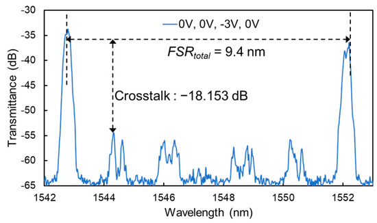
Figure 12.
Experimental drop-port spectral response of fourth-order Vernier MRR filter when −3 V is applied to ring 3.
4.2. Vernier Effect Characteristic
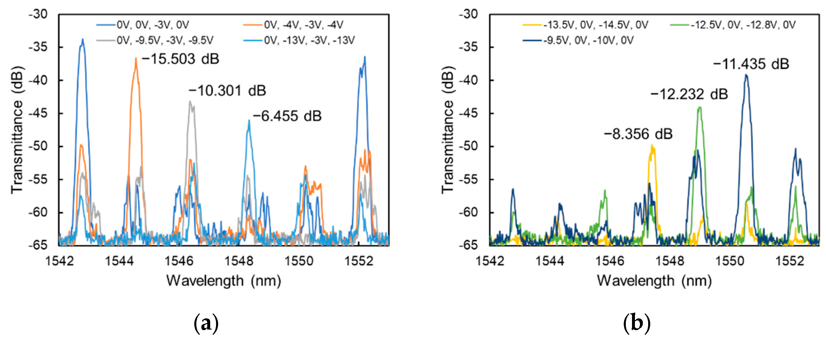
To increase the wavelength channels within one FSR, the MRRs are reverse biased to achieve discrete tuning of the main resonance peak. The main resonance peak shift is shown in Figure 13. When Rings 2 and 4 are applied voltage, the main resonance peak is red-shifted with a step of 1.8 nm, which corresponds to the FSR of Rings 1 and 3, as shown in Figure 13a. In turn, when Rings 2 and 4 are tuned, the main resonance is blue-shifted with a discrete step of 1.5 nm, which corresponds to the FSR of Rings 2 and 4. In WDM systems, a crosstalk of less than −10 dB is required to extract the desired wavelength. Unfortunately, the crosstalk of the main resonance peak is −6.455 dB at a reverse bias of −13 V on Rings 2 and 4, and the crosstalk of the resonance peak is also greater than −10 dB at a reverse bias of −13.5 V and −14.5 V on Rings 1 and 3. The reason is considered to be a manufacturing error in the thickness of each layer in the FACQW core layer during the MOCVD that causes the redshift of the absorption peak with an increase in the applied electric field.
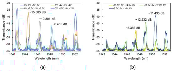
Figure 13.
Vernier tuning of drop port as a function applying voltages to (a) Ring 2 and Ring 4 and (b) Ring 1 and Ring 3.
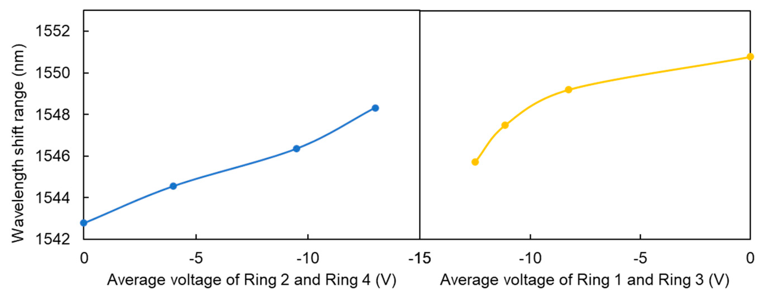
Figure 14 illustrates the wavelength shift range of the main resonance peak as a function of the average voltage applied to MRRs. Excluding the main resonance peaks with crosstalk greater than −10 dB, there are four channels within the FSR. In the right panel of Figure 14, since the reverse bias of Rings 1 and 3 is performed on the premise of Ring 3 at −3 V, the linear tuning is not presented. In the left panel of Figure 14, the discrete tuning of the main resonance peak is close to linear with respect to the applied average voltages to Rings 2 and 4.

Figure 14.
Main resonance peak shift range as a function of the average voltage applied to MRRs.
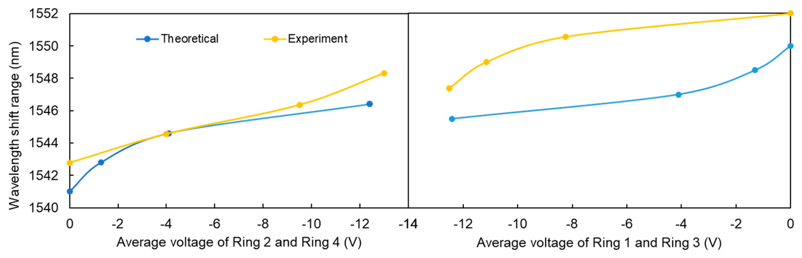
The tuning voltages of the theoretical and experimental values are shown in Figure 14. Since it is necessary to apply a voltage to Ring 3 to align the resonance peaks of Rings 1, 2, and 4, the average voltage of the main resonance peak tuning of Ring 1 and Ring 3 is greater than the theoretical tuning voltage from the right side in Figure 15. Therefore, the theoretical tuning voltage and the experimental tuning voltage are compared with the voltages of Ring 2 and Ring 4. It can be seen from Figure 15 that the experiment tuning voltage is greater than the theoretical tuning voltage in the lower applied voltage range. Its reason can be considered as the impurity density deviation in the waveguide. The electric field-induced refractive index change strongly depends on the impurity densities of the intrinsic FACQW layer and the upper cladding layers. Different impurity densities lead to a large difference in the refractive index change under the same voltage because the electric field-induced refractive index change of the designed FACQW is sensitive to the impurity density. Therefore, the deviation between the impurity density and the designed value in the wafer fabrication is the reason for the increase in the experimental tuning voltage.
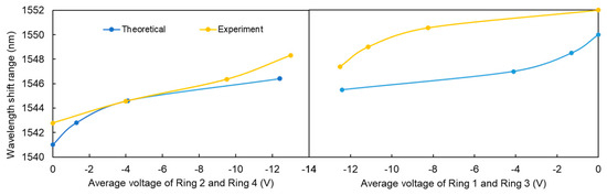
Figure 15.
Comparison of the theoretical and experimental tuning voltage.
4.3. Discussion
The main features of FACQW wafers are easy integration with lasers, low tuning power consumption, and high response speed. The previous work in our group demonstrated the fourth-order microring filter with an FSR of 2 nm and a wavelength tuning range of no more than 1 nm based on the electro-optical effect [26]. When the channel spacing in the WDM system is 0.8 nm, the number of wavelength channels of the FACQW-based fourth-order microring filter with the same round-trip lengths is only one, which will greatly reduce the working efficiency of the FACQW-based MRR filters demonstrated in previous work [26]. The waveguide of FACQW has a large bending loss, and the FSR of FACQW-based MRR filters cannot be increased by reducing the length of MRRs like the Si-based MRR. Therefore, in this study, the relay structure is used in the fourth-order MRR filter. The FSR of the fourth-order Vernier MRR filter is expanded from 2 nm to 9.4 nm, and the individual tuning power consumption of MRRs is less than 150 μW. The number of wavelength channels has increased to 4 from 1. The operation speed of the proposed MRR filter in this study is not measured, but it can be inferred based on the current during wavelength tuning. Currents based on the thermo-optical effect in Si-based MRR filters are usually above milliwatts. The tuning current is microampere, as shown in Figure 7, so the working principle of wavelength tuning is based on the electro-optical effect. According to the operation speed of the previous experiment [26], it can be inferred that the operation speed of the MRR filter in this study is also at the nano-second level.
5. Conclusions and Future Directions
We have demonstrated a fourth-order Vernier MRR filter. The relay structure is adopted, where a busline is placed between MRRs to accurately detect the ring that needs to be tuned due to manufacturing errors. The measured spectral responses show that the FSR is extended to 9.4 nm. The tuning of the MRR filter is driven by the QCSE, and the tuning power required for one MRR is less than 150 μW. Compared to the previous FACQW-based MRR filter with one wavelength channel, the number of wavelength channels is increased to four within one FSR in this study. Ideally, an FSR comparable to the C-band span of 36 nm would be beneficial, as this would increase the number of channels that can be multiplexed and demultiplexed. The FSR based on the FACQW-based filter has been expanded to 9.4 nm, and at least four MRR filters are needed to cover the entire C-band. This is not beneficial to chip miniaturization. In future work, wavelength tuning based on thermo-optical effects and electro-optical effects will be integrated into one MRR filter. The thermo-optical effect is used to achieve a wide range of wavelength shifts, while the electro-optical effect is used to accurately extract wavelength channels within one FSR. This enables MRR filters to cover the entire C-band. In addition, the FACQW wafer needs to be further designed and manufactured to ensure that the resonance peak does not redshift as the voltage increases, so as to achieve six channels within the next FSR under Vernier tuning.
Author Contributions
Conceptualization, Z.P. and T.A.; methodology, Z.P. and T.A.; design and experimental, Z.P.; writing—original draft preparation, Z.P.; review and project administration, T.A. All authors have read and agreed to the published version of the manuscript.
Funding
This research was funded by the Ministry of Education, Culture, Sports, Science and Technology of Japan (21H01841).
Institutional Review Board Statement
Not applicable.
Informed Consent Statement
Not applicable.
Data Availability Statement
Data are contained within the article.
Acknowledgments
The authors thank ARIM Japan (JPMXP1222UT1049) for supporting the experimentation.
Conflicts of Interest
The authors declare no conflict of interest.
References
- Madsen, C.K.; Lenz, G.; Bruce, A.J.; Capuzzo, M.A.; Gomez, L.T.; Nielsen, T.N.; Brener, I. Multistage dispersion compensator using ring resonators. Opt. Lett. 1999, 24, 1555–1557. [Google Scholar] [CrossRef]
- Fan, Y.; Epping, J.P.; Oldenbeuving, R.M.; Roeloffzen, C.G.; Hoekman, M.; Dekker, R.; Heideman, R.G.; van der Slot, P.J.; Boller, K.J. Optically Integrated InP–Si3N4 Hybrid Laser. IEEE Photon. J. 2016, 8, 1505111. [Google Scholar] [CrossRef]
- Wei, H.; Krishnaswamy, S. Polymer micro-ring resonator integrated with a fiber ring laser for ultrasound detection. Opt. Lett. 2017, 42, 2655–2658. [Google Scholar] [CrossRef] [PubMed]
- Sakai, K.; Kato, S.; Yoshikawa, N.; Kokubun, Y.; Arakawa, T. Proposal of ultra-low voltage quantum well optical modulator for optical interconnection in superconducting integrated circuit systems. J. Appl. Phys. 2020, 59, SOOB01. [Google Scholar] [CrossRef]
- Wu, Z.; Chen, Y.; Zhang, T.; Shao, Z.; Wen, Y.; Xu, P.; Zhang, Y.; Yu, S. Design and optimization of optical modulators based on graphene-on-silicon nitride microring resonators. J. Opt. 2017, 19, 045801. [Google Scholar] [CrossRef]
- Waldow, M.; Plötzing, T.; Gottheil, M.; Först, M.; Bolten, J.; Wahlbrink, T.; Kurz, H. 25ps all-optical switching in oxygen implanted silicon-on-insulator microring resonator. Opt. Express 2008, 16, 7693–7702. [Google Scholar] [CrossRef] [PubMed]
- Pelc, J.S.; Rivoire, K.; Vo, S.; Santori, C.; Fattal, D.A.; Beausoleil, R.G. Picosecond all-optical switching in hydrogenated amorphous silicon microring resonators. Opt. Express 2014, 22, 3797–3810. [Google Scholar] [CrossRef]
- Katti, R.; Prince, S. Photonic delay lines based on silicon coupled resonator optical waveguide structures. Silicon 2018, 10, 2793–2800. [Google Scholar] [CrossRef]
- Dey, S. Optical hextuple ring resonator-based delay line architecture. J. Opt. 2022, 51, 106–114. [Google Scholar] [CrossRef]
- Liu, S.; Shoji, Y.; Mizumoto, T. TE-mode magneto-optical isolator based on an asymmetric microring resonator under a unidirectional magnetic field. Opt. Express 2022, 30, 9934–9943. [Google Scholar] [CrossRef]
- Pintus, P.; Huang, D.; Zhang, C.; Shoji, Y.; Mizumoto, T.; Bowers, J.E. Microring-based optical isolator and circulator with integrated electromagnet for silicon photonics. J. Light. Technol. 2017, 35, 1429–1437. [Google Scholar] [CrossRef]
- Saharia, A.; Mudgal, N.; Choure, K.K.; Maddila, R.; Tiwari, M.; Singh, G. Proposed all-optical read-only memory element employing Si3N4 based optical microring resonator. Optik 2022, 25, 168493. [Google Scholar] [CrossRef]
- Gu, J.; Feng, C.; Zhao, Z.; Ying, Z.; Liu, M.; Chen, R.T.; Pan, D.Z. SqueezeLight: Towards scalable optical neural networks with multi-operand ring resonators. In Proceedings of the Design, Automation Test in Europe Conference Exhibition (DATE), Grenoble, France, 1–5 February 2021; pp. 238–243. [Google Scholar]
- Matsuura, S.; Yamasaku, N.; Nishijima, Y.; Okazaki, S.; Arakawa, T. Characteristics of highly sensitive hydrogen sensor based on Pt-WO3/Si microring resonator. Sensors 2019, 20, 96. [Google Scholar] [CrossRef] [PubMed]
- Yamasaku, N.; Matsuura, S.; Nishijima, Y.; Arakawa, T.; Okazaki, S. Response Characteristics of Silicon Microring Resonator Hydrogen Sensor. Proceedings 2018, 2, 795. [Google Scholar]
- Barwicz, T.; Popovic, M.A.; Rakich, P.T.; Watts, M.R.; Haus, H.A.; Ippen, E.P.; Smith, H.I. Microring-resonator-based add-drop filters in SiN: Fabrication and analysis. Opt. Express 2004, 12, 1437–1442. [Google Scholar] [CrossRef]
- Ding, Y.; Tao, S.; Wang, X.; Shang, C.; Pan, A.; Zeng, C.; Xia, J. Thermo-optic tunable optical filters with GHz-bandwidth and flat-top passband on thin film lithium niobate platform. Opt. Express 2022, 30, 22135–22142. [Google Scholar] [CrossRef] [PubMed]
- Samanta, S.; Dey, P.K.; Banerji, P.; Ganguly, P. Development of micro-ring resonator-based optical bandpass filter using SU-8 polymer and optical lithography. Opt. Mater. 2018, 77, 122–126. [Google Scholar] [CrossRef]
- Liu, D.; Zhang, C.; Liang, D.; Dai, D. Submicron-resonator-based add-drop optical filter with an ultra-large free spectral range. Opt. Express 2019, 27, 416–422. [Google Scholar] [CrossRef] [PubMed]
- Hu, T.; Wang, W.; Qiu, C.; Yu, P.; Qiu, H.; Zhao, Y.; Jiang, X.; Yang, J. Thermally tunable filters based on third-order microring resonators for WDM applications. IEEE Photon. Technol. Lett. 2012, 24, 524–526. [Google Scholar] [CrossRef]
- Liu, L.; Xue, W.; Jin, X.; Yue, J.; Yu, Z.; Zhou, L. Bandwidth and wavelength tunable all-optical filter based on cascaded opto-mechanical microring resonators. IEEE Photon. J. 2019, 11, 7800210. [Google Scholar] [CrossRef]
- Arakawa, T.; Toya, T.; Ushigome, M.; Yamaguchi, K.; Ide, T.; Tada, K. InGaAs/InAlAs five-layer asymmetric coupled quantum well exhibiting giant electrorefractive index change. Jpn. J. Appl. Phys. 2011, 50, 032204. [Google Scholar] [CrossRef]
- Ikehara, H.; Goto, T.; Kamiya, H.; Arakawa, T.; Kokubun, Y. Hitless wavelength-selective switch based on quantum well second-order series-coupled microring resonators. Opt. Express 2013, 21, 6377–6390. [Google Scholar] [CrossRef] [PubMed]
- Arakawa, T.; Hariki, T.; Amma, Y.; Fukuoka, M.; Ushigome, M.; Tada, K. Low-voltage Mach–Zehnder modulator with InGaAs/InAlAs five-layer asymmetric coupled quantum well. Jpn. J. Appl. Phys. 2012, 51, 042203. [Google Scholar] [CrossRef]
- Makino, T.; Gotoh, T.; Hasegawa, R.; Arakawa, T.; Kokubun, Y. Microring resonator wavelength tunable filter using five-layer asymmetric coupled quantum well. J. Light. Technol. 2011, 29, 2387–2393. [Google Scholar] [CrossRef]
- Kamiya, H.; Goto, T.; Ikehara, H.; Katouf, R. Arakawa, and Y. Kokubun. Hitless wavelength-selective switch with quadruple series-coupled microring resonators using multiple-quantum-well waveguides. Opt. Express 2013, 21, 20837–20850. [Google Scholar] [CrossRef]
- Zhou, L.; Zhang, X.; Lu, L.; Chen, J. Tunable Vernier Microring Optical Filters With p-i-p-Type Microheaters. IEEE Photon. J. 2013, 5, 6601211. [Google Scholar] [CrossRef]
- Boeck, R.; Jaeger, N.A.; Rouger, N.; Chrostowski, L. Series-coupled silicon racetrack resonators and the Vernier effect: Theory and measurement. Opt. Express 2010, 18, 25151–25157. [Google Scholar] [CrossRef]
- Goebuchi, Y.; Kato, T.; Kokubun, Y. Optimum arrangement of high-order series-coupled microring resonator for crosstalk reduction. J. Appl. Phys. 2006, 45, 5769. [Google Scholar] [CrossRef]
- Peng, Z.; Komatsubara, T.; Yamauchi, M.; Arakawa, T. Design of a series-coupled microring resonator wavelength filter using the digital filter design method. J. Opt. Soc. B. 2021, 38, 2837–2846. [Google Scholar] [CrossRef]
- Chaichuay, C.; Yupapin, P.P.; Saeung, P. The serially coupled multiple ring resonator filters and Vernier effect. Opt. Appl. 2009, 39, 174. [Google Scholar]


Disclaimer/Publisher’s Note: The statements, opinions and data contained in all publications are solely those of the individual author(s) and contributor(s) and not of MDPI and/or the editor(s). MDPI and/or the editor(s) disclaim responsibility for any injury to people or property resulting from any ideas, methods, instructions or products referred to in the content. |
© 2023 by the authors. Licensee MDPI, Basel, Switzerland. This article is an open access article distributed under the terms and conditions of the Creative Commons Attribution (CC BY) license (https://creativecommons.org/licenses/by/4.0/).