Communication

Design of a Novel Broadband Antenna for Photomixer Chips in the Terahertz Frequency Range

1
Key Laboratory of Optoelectronic Materials and Devices, Institute of Semiconductors, Chinese Academy of Sciences, Beijing 100083, China
2
College of Materials Science and Optoelectronic Technology, University of Chinese Academy of Sciences, Beijing 100049, China
3
School of Electronic, Electrical and Communication Engineering, University of Chinese Academy of Sciences, Beijing 100049, China
*
Authors to whom correspondence should be addressed.
Photonics 2023, 10(12), 1321; https://doi.org/10.3390/photonics10121321
Submission received: 28 October 2023 / Revised: 22 November 2023 / Accepted: 28 November 2023 / Published: 29 November 2023

Abstract

:
A novel broadband antenna designed for the terahertz (THz) frequency range is proposed and developed for the THz emitter on a photomixer chip. This THz emitter comprises an ultra-high-speed indium phosphide photodetector integrated with a planar THz antenna. This paper presents a novel broadband antenna configuration comprising a combination of bowtie and circular patch elements designed for the frequency range of 150 GHz to 500 GHz. Detailed parametric analysis of the antenna’s design parameters is also provided. The simulation results demonstrate that the optimized antenna achieves an impedance bandwidth of 350 GHz, satisfying the |S11| ≤ −10 dB condition, and exhibits a relative bandwidth of 107% within the 150 GHz to 500 GHz frequency range. This novel broadband terahertz antenna showcases an exceptional wideband performance and is highly suitable for high-speed transmission systems.

1. Introduction

With the rapid growth in information demand and escalating data communication traffic [1,2], traditional communication systems operating in lower frequency bands no longer suffice to meet society’s requirements. The inevitable trend is the expansion of carrier frequencies towards higher frequency ranges. The terahertz (THz) band represents a largely unexplored domain offering vast potential applications and developmental opportunities. Terahertz waves, situated within the electromagnetic spectrum from 0.1 THz to 10 THz, possess unique advantages for communication, including short wavelengths and ample available bandwidth, rendering them pivotal in future wireless communication systems [3,4,5,6]. In comparison to the millimeter-wave band, the terahertz frequency range promises to provide significantly larger usable bandwidth, advancing by an order of magnitude. In the terahertz spectrum, the low terahertz frequency range (100 GHz–1 THz) imposes relatively modest technical requirements on devices while preserving the unique characteristics of terahertz waves. Therefore, low terahertz technology is poised to offer unprecedented data rates in future generations of wireless systems, particularly in the context of the sixth-generation (6G) mobile communication systems [7].
The microwave photonics terahertz communication system based on optoelectronic integration effectively harnesses the wide bandwidth advantages of the terahertz spectrum. It combines optical fiber broadband communication with wireless communication, making it highly promising to serve as a fundamental technology for future integrated high-speed optoelectronic networks [8]. The key component of this system is the terahertz radiation source based on a photomixer module [4], which consists of a high-speed optoelectronic detector integrated with a THz resonant antenna. In this photonic terahertz radiation source, two distinct frequency optical beams mix within a uni-traveling-carrier photodetector [9,10], generating a THz signal with a frequency equal to the difference between the frequencies of the incident optical beams. This THz signal is then radiated via a THz antenna integrated with the photodetector [10,11,12]. These sources are extensively researched due to their advantages, including room-temperature continuous operation, wideband tunability, and high spectral purity [13].
In order to achieve high-performance terahertz sources, we need a terahertz antenna with broadband characteristics. In addition, the antenna also needs to have the characteristics of plane geometry, so that we can integrate the antenna and the photodetector on the chip [14]. Microstrip antennas can be easily designed to produce a variety of radiation patterns and polarizations and depend on the shape (circular, rectangular, etc.) [15]. However, the main disadvantage of microstrip antennas compared to other types of antenna designs is that they have a single-band performance, but not a broadband performance. Among various antenna configurations, the bowtie antenna has been widely concerned in recent years for its advantages of good broadband characteristics, simple and compact structure, and easy realization [16,17]. We can combine two or more antennas together to obtain better broadband characteristics.
At the 2019 World Radiocommunication Conference, the unrestricted allocation of terahertz bandwidth resources for fixed and land mobile service applications was approved within the frequency ranges of 275–296 GHz, 306–313 GHz, 318–333 GHz, and 356–450 GHz [18]. At present, for terahertz communication, researchers are focusing more on the low terahertz frequency range of 100 GHz to 500 GHz [19,20,21]. Therefore, we expect to obtain a novel combined high-performance terahertz antenna for the 100 GHz to 500 GHz band that can provide at least a 100% relative bandwidth.
This paper introduces a novel broadband antenna configuration, comprising bowtie and circular patch, designed for the 150 GHz–500 GHz terahertz frequency range. We conducted simulation analysis of the proposed novel antenna and optimized its radiation characteristics via detailed parametric investigations of various design parameters. The proposed wideband antenna design achieved an impedance bandwidth of 350 GHz.
This paper is organized as follows: Section 2 provides a detailed exposition of the antenna’s design process, Section 3 outlines the optimization analysis of the antenna’s design parameters, Section 4 describes the radiation performance of the optimized antenna, and finally, Section 5 summarizes key findings from this research.

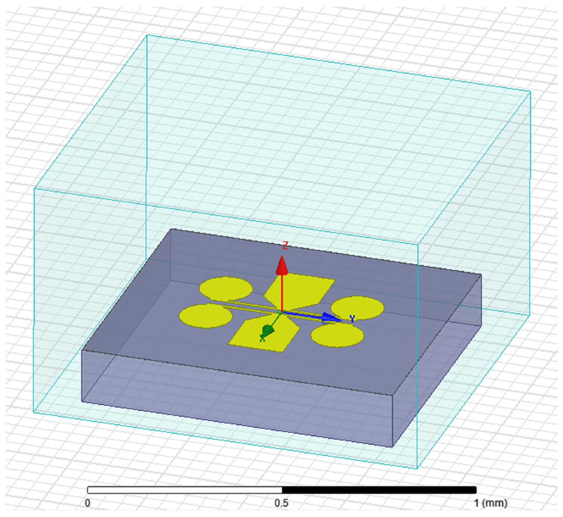
2. Antenna Design Procedure

The antenna design proposed in this paper is illustrated in Figure 1. It consists of a pair of bowtie antenna and two pairs of circular patch antennas. The central symmetric region of the bowtie antenna and circular patch antenna serves as the antenna’s feed area, which is also the emission source. In this region, indium phosphide (InP) photodetectors facilitate the optoelectronic conversion process. The metallic conductor of the antenna is composed of gold material with a thickness denoted as “t”. Beneath the antenna lies a substrate comprising an indium phosphide layer (with a relative dielectric constant of 10.8) and a thin layer of silicon dioxide dielectric (with a relative dielectric constant of 4) positioned above the indium phosphide layer.
Broadband antennas typically require intricate structures to achieve responses across multiple frequencies. In this paper, the complexity of the antenna primarily arises from the geometric structure of the combined antennas. The bowtie antenna, as a component of the novel antenna design, relies on its non-resonant structure and multimodal radiation characteristics as key factors for achieving a broadband performance [22]. Meanwhile, although the circular patch antenna is inherently a narrowband antenna, it can resonate at multiple frequencies, and the selection of resonance modes is related to parameters such as the radius of the circular patch [23,24]. We chose to introduce design elements of circular patches on the basis of the bowtie antenna, adding complexity to the geometric structure but bringing forth a more diverse range of resonance modes.
We established a 3D simulation model for the proposed novel bowtie and circular patch combination terahertz antenna, as depicted in Figure 2. The feeding region employed a lumped port excitation method with dimensions of 20 × 20 µm2, and the port impedance was set to 50 ohms. The substrate’s bottom and the metal surface of the antenna’s main body were designated as perfect conductor boundary conditions, while the external air cavity adopted radiation boundary conditions. A comprehensive parametric simulation was conducted on the entire model using a time-domain solver. Preliminary numerical analysis of this innovative antenna was performed and the initial simulation dimensions of the antenna are presented in Table 1. The subsequent section will further analyze the impact of parameter variations in the antenna’s dimensions on its performance.

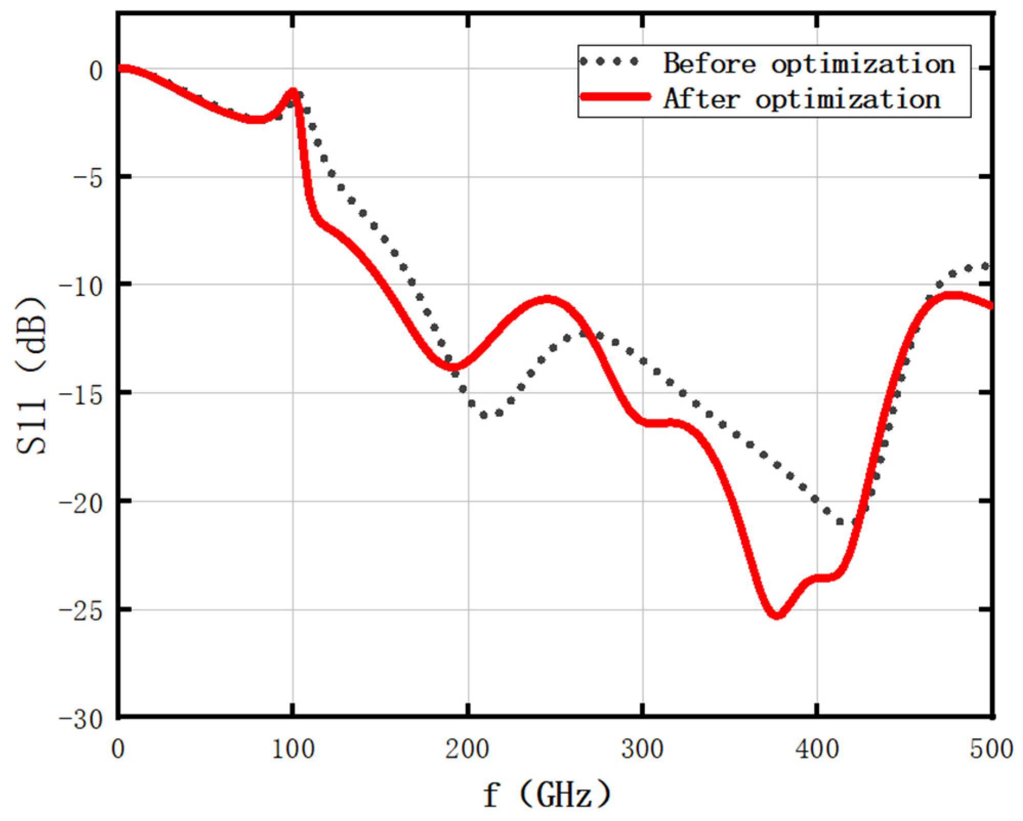
3. Optimization of Broadband Terahertz Antennas

In this section, a detailed simulation and optimization analysis of the novel composite antenna shown in Figure 1 has been conducted. The primary focus of the modeling is an extensive analysis of the impact of various antenna design parameters on the antenna’s reflection coefficient (S11). Antennas typically require an S11 value of less than −10 dB, signifying a return loss exceeding 10 dB, indicating minimal signal energy reflection.
The optimization analysis involved carefully selecting the range of variations for various design parameters, taking into account manufacturing constraints to minimize the substantial memory requirements of numerical models with various parameter sets. The upper and lower limits of each parameter are selected by covering the maximum value range without affecting the antenna shape. In all parametric analysis, we have provided significant parameter values, which give the important behavior by taking into account the fabrication constraints.

3.1. Effect of Substrate Thickness

Due to the substrate’s thickness (h) typically exceeding the wavelength of terahertz waves, the generation of surface/substrate modes is a phenomenon that cannot be disregarded. Beneath the antenna, the substrate consists of an indium phosphide layer (with a relative dielectric constant of 10.8) having a thickness denoted as d2, with a thin layer of silicon dioxide dielectric (with a relative dielectric constant of 4) positioned immediately above the indium phosphide layer, having a thickness of d1.
Figure 3 depicts the impact of varying the silicon dioxide substrate thickness (d1) from 0.3 μm to 0.6 μm on the reflection parameters of the designed antenna. For various d1 values, the antenna’s S11 remains consistently below −10 dB within the 150 GHz–470 GHz frequency range. As the silicon dioxide substrate thickness increases from 0.3μm to 0.6 μm, only minimal variations are observed in the antenna’s reflection parameter S11, with the overall curve shifting slightly towards the upper right. When the substrate thickness is 0.3 μm, the maximum frequency range complying with S11 < −10 dB is achieved, resulting in an impedance bandwidth of 350 GHz (150 GHz–500 GHz), showcasing the antenna’s optimal performance at this dimension.
Figure 4 showcases the impact of altering the indium phosphide substrate thickness (d2) from 130 μm to 160 μm on the reflection parameters of the designed antenna. As the indium phosphide substrate thickness increases from 130 μm to 160 μm, there is minimal fluctuation in the antenna’s reflection parameter S11. For d2 values of 140 μm, 150 μm, and 160 μm, all satisfy the condition S11 < −10 dB within the 150 GHz–500 GHz frequency band. Consequently, we opt for an indium phosphide substrate thickness of d2 = 140 μm as the ultimate optimization outcome.

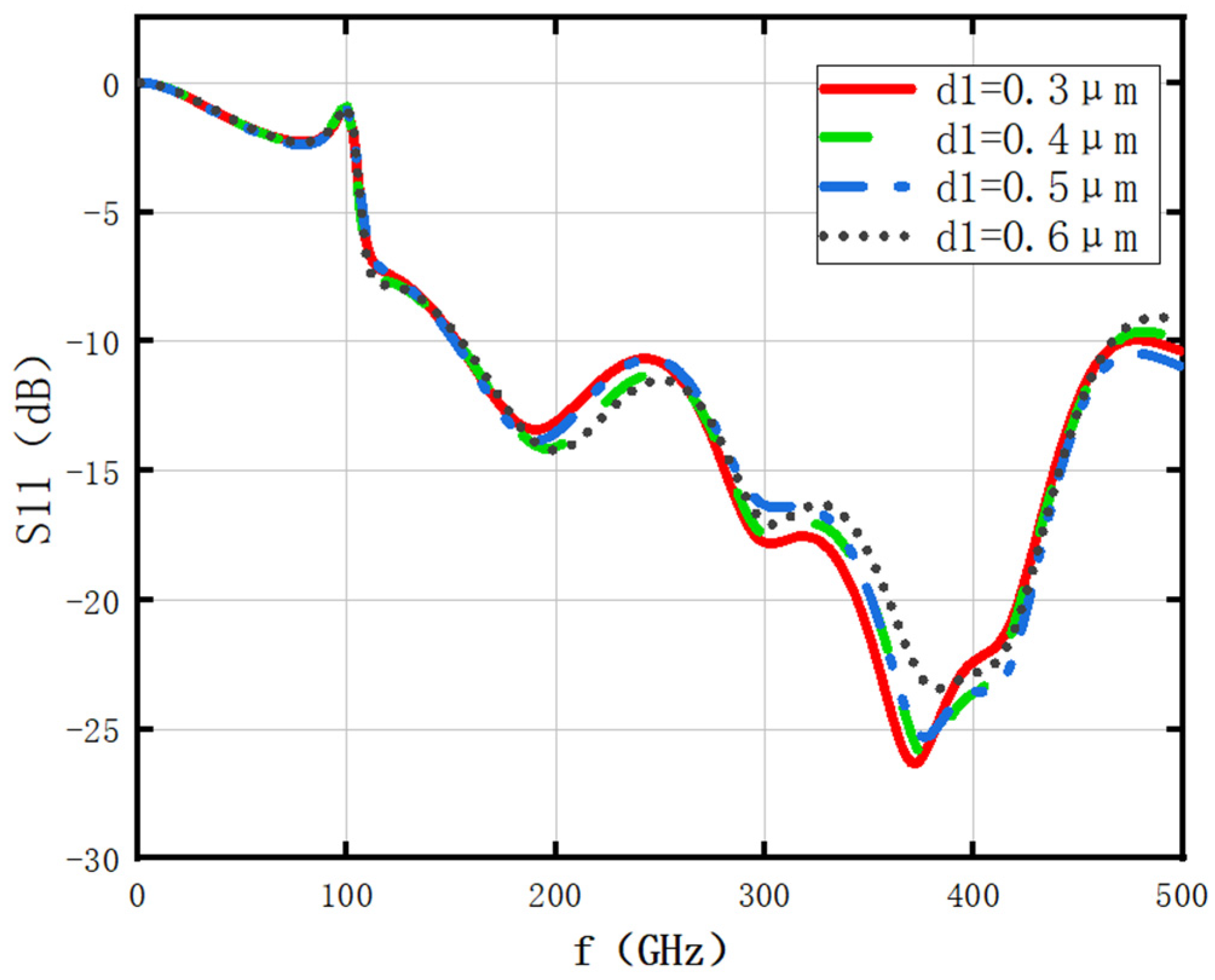
3.2. Effect of Gold Thickness

Figure 5 illustrates the impact of gold thickness (t) varying from 0.3 μm to 0.9 μm on the reflection parameters of the designed antenna. The change in gold thickness between 0.3 µm and 0.9 µm leads to a significant 5 dB variation in S11 within the 150 GHz~500 GHz band. The antenna’s reflection characteristics are sensitive to the variations in gold thickness (t) due to the changes in the current distribution along the antenna affecting its resonance characteristics. From Figure 4, the optimal metal thickness for achieving the best resonance characteristics is determined to be 0.9 μm.

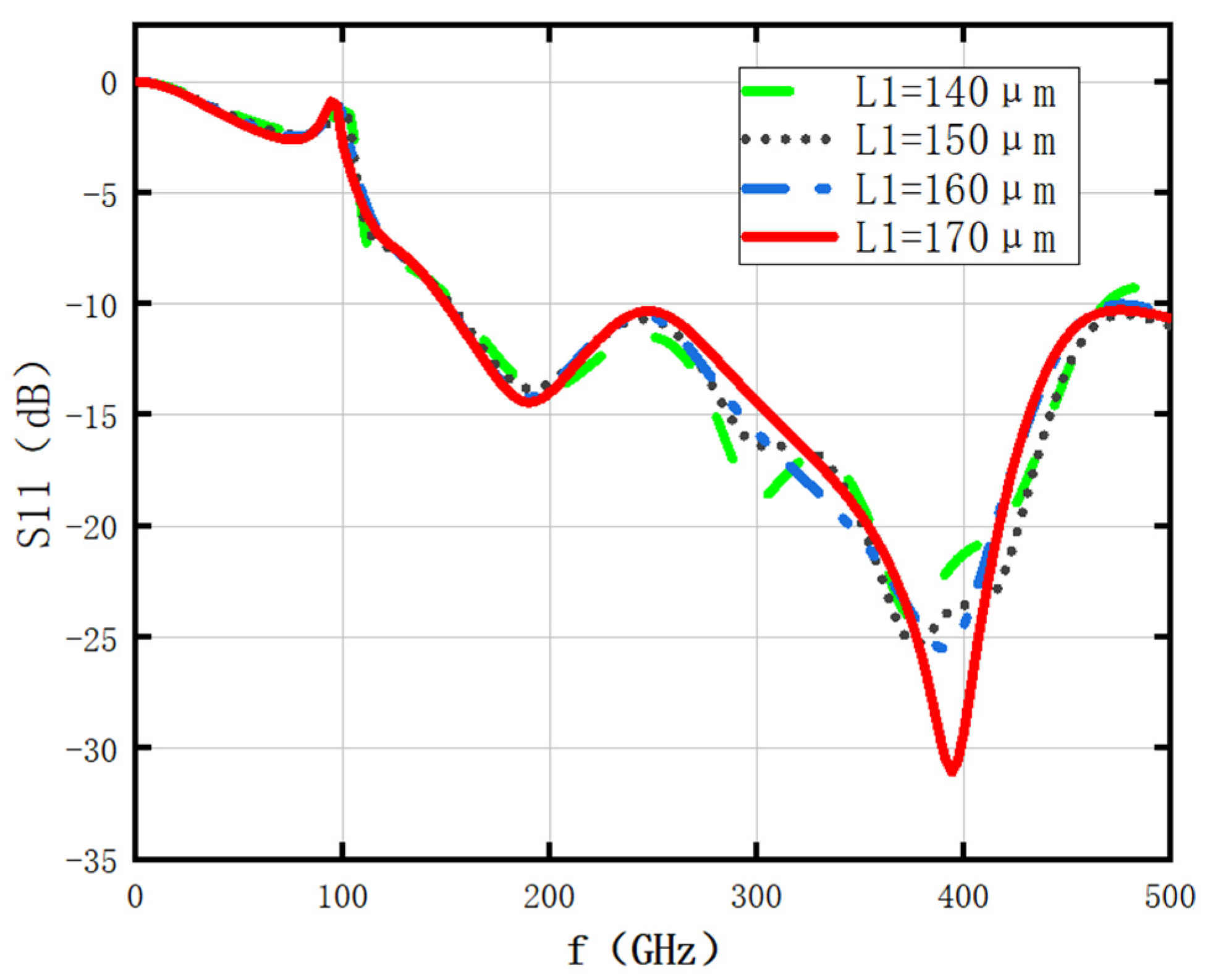
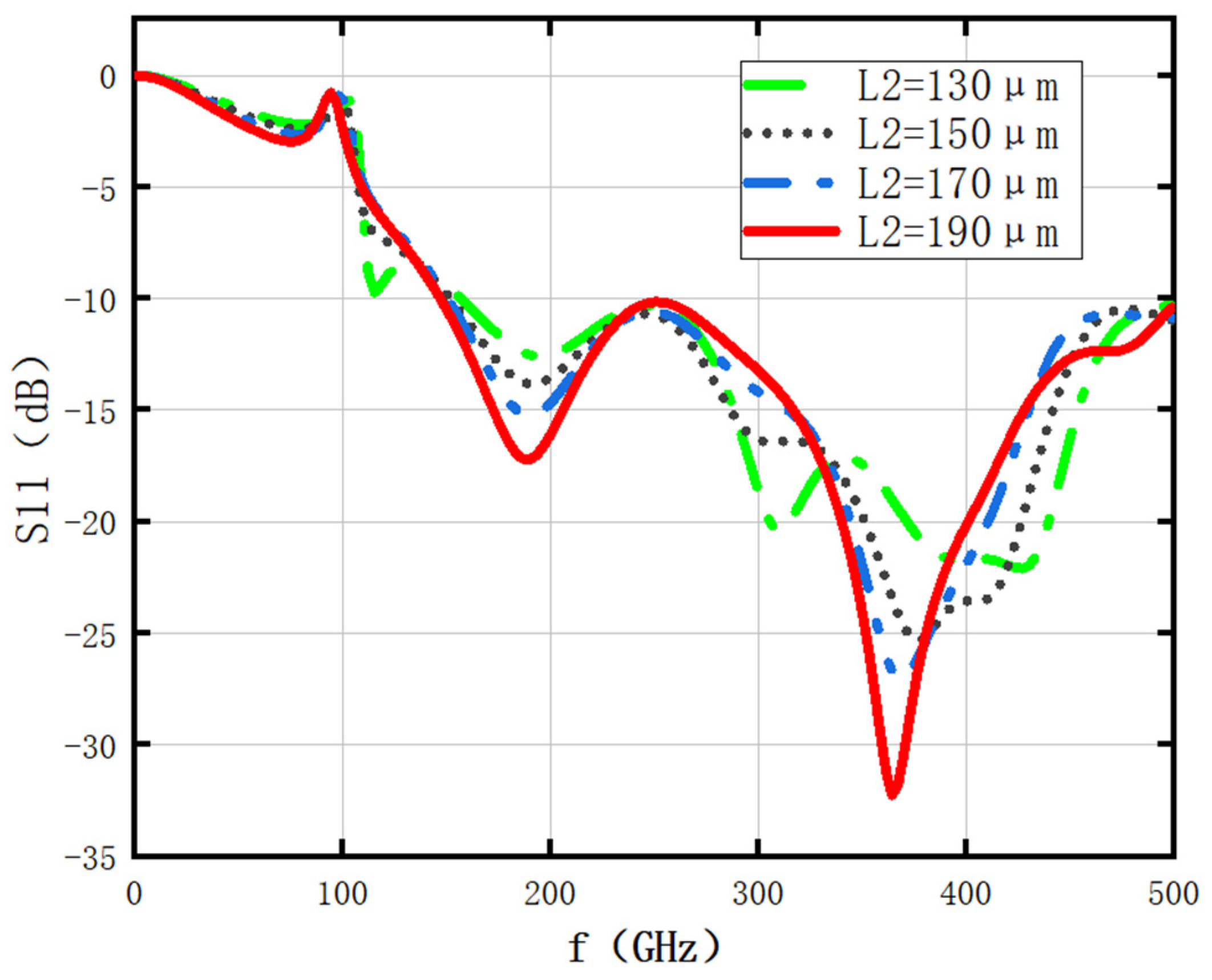
3.3. Effect of Bowtie Patch Antenna Dimensions

The antenna dimension design is divided into three parts: the first part involves optimizing the dimensions of the bowtie patch antenna, the second part concerns optimizing the dimensions of the circular patch antenna, and the third part focuses on designing the dimensions of the microstrip lines connecting them. First, we optimized two parameters of the bowtie patch antenna: width (L1) and length (L2).
Figure 6 shows the impact of varying the width (L1) of the bowtie patch antenna from 140 μm to 170 μm on the antenna’s reflection parameters. When the width of the bowtie patch antenna varies between 140 µm and 160 µm, there is minimal variation in the numerical values of S11, making this change negligible. However, at a width of 170 μm, a noticeable decrease in S11’s valley point is observed. Consequently, we select L1 = 170 μm.
Figure 7 illustrates the impact of varying the length (L2) of the bowtie patch antenna from 130 μm to 190 μm on the antenna’s reflection parameters. Changes in L2 within the range of 130 μm to 190 μm cause the valley points of the S11 curves to shift towards lower frequencies and decrease in magnitude. However, all four curves satisfy S11 < −10 dB within the 150 GHz~500 GHz frequency range. Ultimately, we choose L2 = 190 μm as the optimized result due to its minimal S11 value at the valley point.

3.4. Effect of Circular Patch Antenna Radius

The second step in designing the antenna’s dimensions is determining the dimensions of the circular patch antenna, specifically its radius (R). Figure 8 illustrates the impact of varying R on the antenna’s S11. As R varies within the range of 60 μm to 90 μm, the S11 curves exhibit significant frequency-dependent variations. Within the 150 GHz~500 GHz band, the curve that provides both a wide bandwidth and the lowest S11 value corresponds to R = 70 μm.

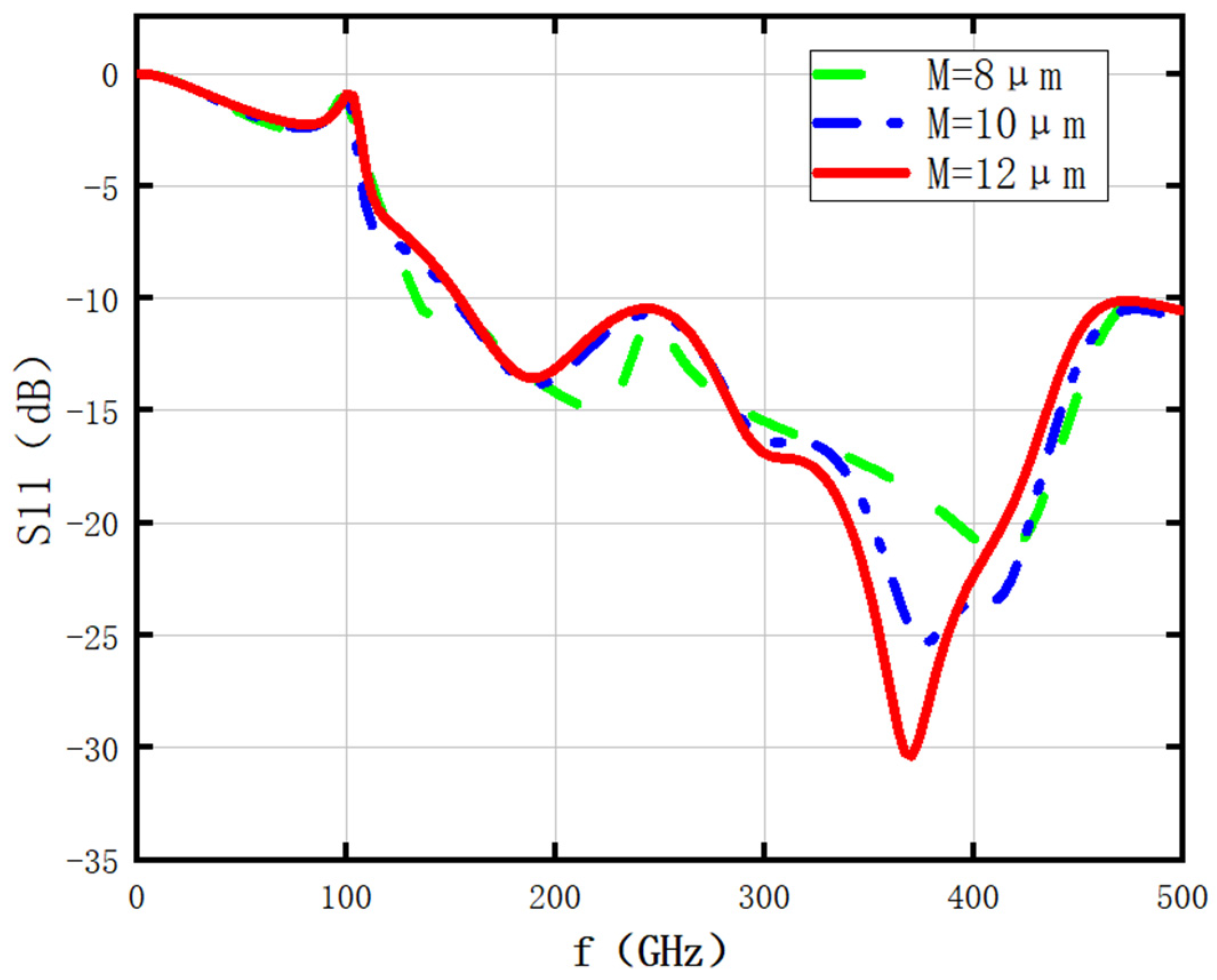
3.5. Effect of Microstrip Line Dimensions

The third step in antenna dimension design is optimizing the dimensions of the microstrip lines, including length (H) and width (M).
Figure 9 displays the effect of varying the length (H) of the microstrip lines from 190 μm to 220 μm on the antenna’s S11. As H increases from 190 μm to 220 μm, a substantial shift of the S11 curves towards lower frequencies is observed. Considering the requirement for a wide bandwidth, we select H = 200 μm as the optimal result.
Figure 10 shows the impact of varying the width (M) of the microstrip lines from 8 μm to 12 μm on the antenna’s S11. As M changes within this range, the valley points of the S11 curves reduce in magnitude and shift towards lower frequencies. However, all three curves maintain S11 < −10 dB within the 150 GHz~500 GHz frequency range. Ultimately, we choose M = 12 μm as the optimal result, corresponding to the smallest S11 value at the valley point.
Table 2 presents the optimized design parameters of the novel broadband terahertz antenna based on a parametric study. The subsequent analysis uses these parameters to evaluate the antenna’s radiation performance in the far-field region.

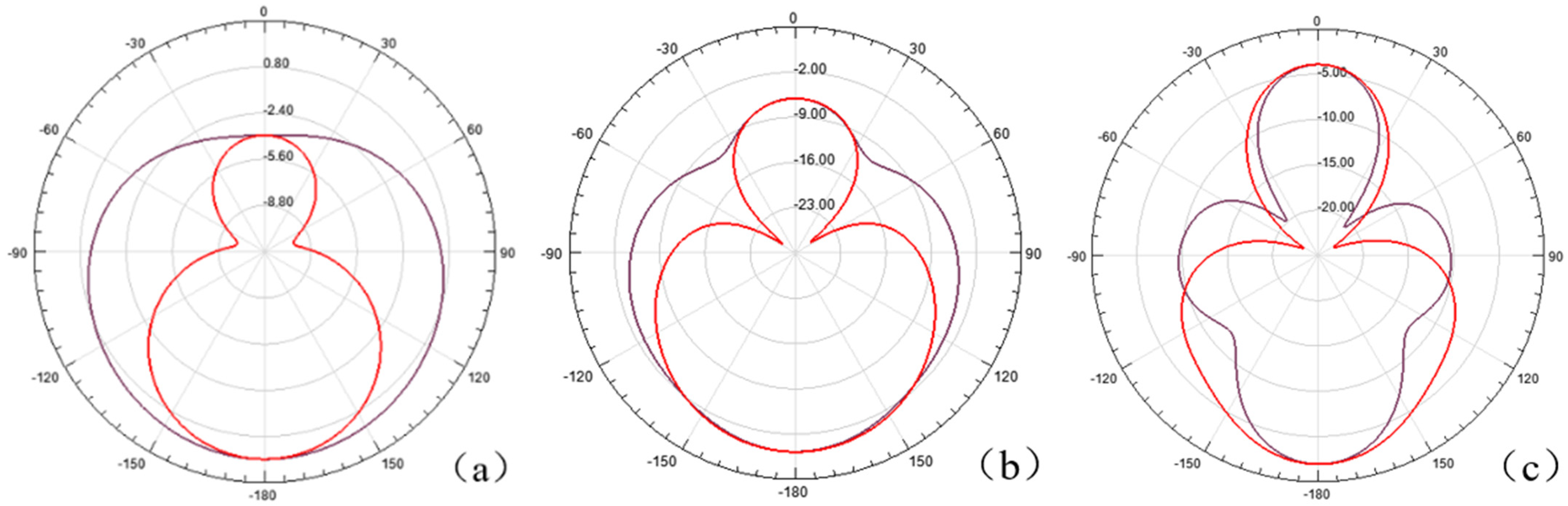
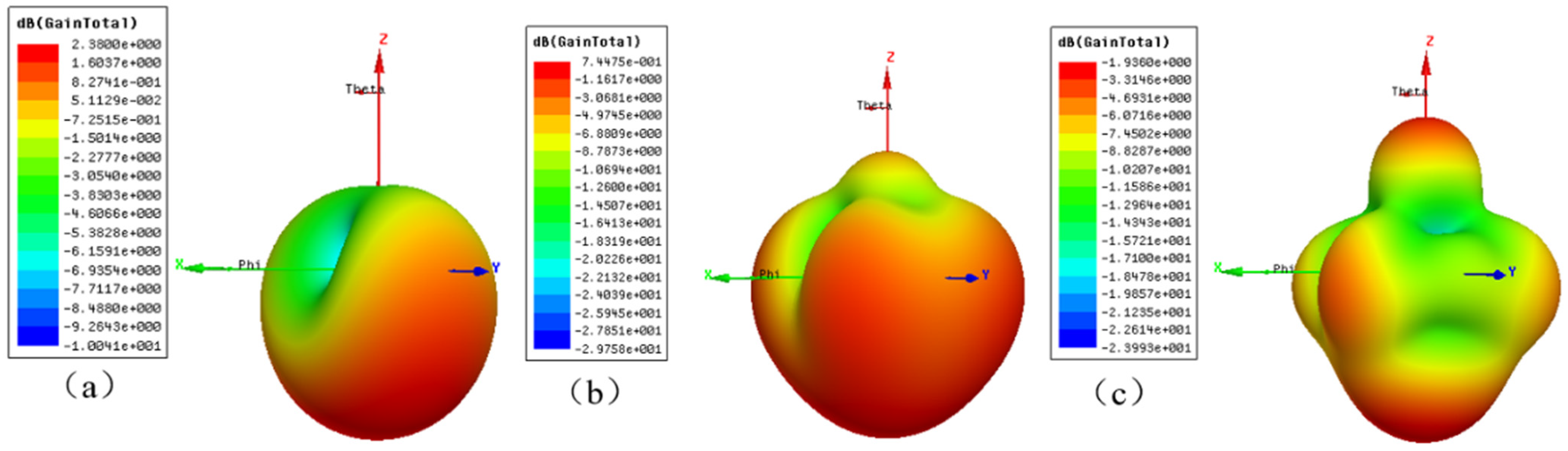
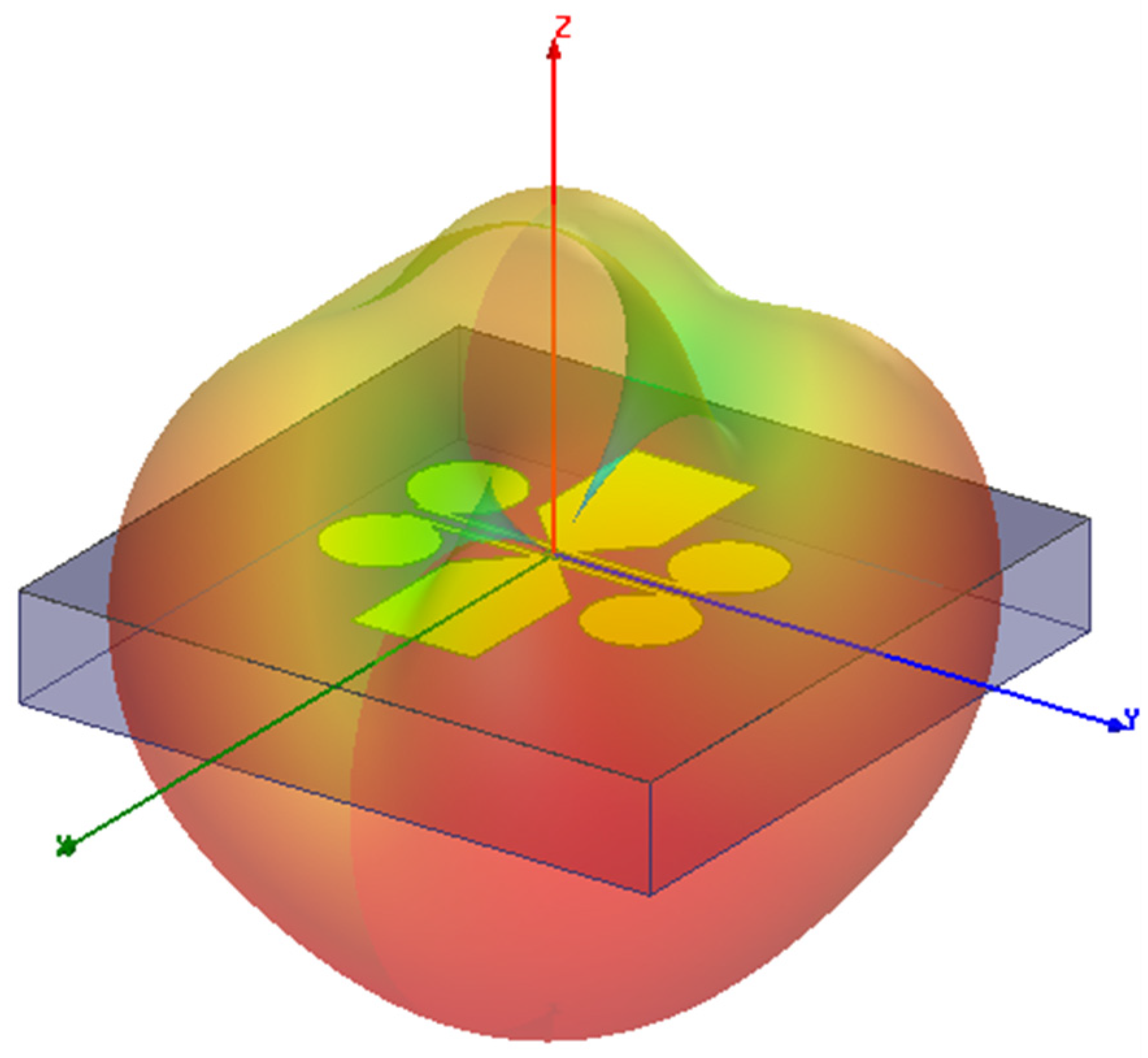
4. Optimized Antenna Radiation Performance

Figure 11 illustrates the changes in the antenna’s reflection coefficient (S11) before and after optimization. Through simulation optimization, we successfully increased the impedance bandwidth of the antenna from 300 GHz to 350 GHz, and the relative bandwidth from 94% to 107%.
Antennas with an impedance bandwidth greater than or equal to 500 MHz or a fractional bandwidth (FBW) greater than 20% are typically referred to as ultra-wideband (UWB) antennas [25]. For the proposed novel bowtie and circular patch combination terahertz antenna, the −10 dB impedance bandwidth (|S11| ≤ −10 dB) and FBW are approximately 350 GHz and 107%, respectively.
We utilized the optimized antenna design parameters to simulate the far-field radiation performance of the antenna. Figure 12a–c respectively depicts the two-dimensional radiation patterns of the antenna at frequencies of 180 GHz, 285 GHz, and 350 GHz. All three figures illustrate that the main lobe of the antenna is directed below the substrate (−180°) and the pattern exhibits near-axial symmetry. Figure 13a–c illustrates the simulated far-field radiation patterns of the antenna at frequencies of 180 GHz, 285 GHz, and 350 GHz. Figure 14 presents an overlay of the antenna’s radiation patterns and the design diagram, providing a general visualization of the antenna’s far-field radiation characteristics.

5. Comparison with State of the Art

Table 3 presents a comparison between the proposed terahertz novel antenna in this study and previous broadband terahertz antennas. In prior designs, these terahertz antennas exhibited certain limitations in terms of impedance bandwidth and relative bandwidth in the low terahertz frequency range. In contrast, the optimized novel combination of the bowtie and circular patch antenna that we designed boasts an impressive 350 GHz impedance bandwidth with a remarkable relative bandwidth of 107%. This table distinctly illustrates that our novel antenna in this work outperforms previous terahertz antennas in terms of an outstanding broadband performance.

6. Conclusions

This paper presents a novel terahertz broadband antenna designed for the low terahertz frequency range of 150 GHz to 500 GHz. A comprehensive parametric analysis of the antenna’s design parameters was conducted, resulting in the optimal design parameters for the proposed antenna. The optimized novel combination of bowtie and circular patch in the designed broadband antenna achieves an impressive impedance bandwidth of 350 GHz with a relative bandwidth of 107%. The broad bandwidth in the low terahertz frequency range allows for the antenna to simultaneously cover multiple frequency points, enhancing system flexibility and adaptability. When employed in high-speed transmission systems, this antenna enables a higher data transfer rate.

Author Contributions

Formal analysis, Y.C., H.Y. and Q.H.; funding acquisition, Q.H., H.Y. and S.W.; methodology, Y.C. and Q.H.; software, Y.C.; writing—original draft, Y.C.; writing—editing, Q.H., H.Y., S.W., Y.Z. and L.G. All authors have read and agreed to the published version of the manuscript.

Funding

This study was funded by the National key Research and Development program of China (Grant No. 2020YFB1805701) and the National Natural Science Foundation of China (Grant Nos. 61934003).

Institutional Review Board Statement

Not applicable.

Informed Consent Statement

Not applicable.

Data Availability Statement

The data that support the findings of this study are available from the. corresponding author upon reasonable request.

Conflicts of Interest

The authors declare no conflict of interest.

References

  1. Zhou, X.; Liu, H.; Urata, R.; Zebian, S. Scaling Large Data Center Interconnects: Challenges and Solutions. Opt. Fiber Technol. 2018, 44, 61–68. [Google Scholar] [CrossRef]
  2. Miguelez, P. What Applications Are Driving Higher Capacity in Access? In Proceedings of the Optical Fiber Communication Conference (2018), San Diego, CA, USA, 11 March 2018; Optica Publishing Group: Washington, DC, USA, 2018; p. M2B.1. [Google Scholar]
  3. Akyildiz, I.F.; Jornet, J.M.; Han, C. Terahertz Band: Next Frontier for Wireless Communications. Phys. Commun. 2014, 12, 16–32. [Google Scholar] [CrossRef]
  4. Kleine-Ostmann, T.; Nagatsuma, T. A Review on Terahertz Communications Research. J. Infrared Milli. Terahz. Waves 2011, 32, 143–171. [Google Scholar] [CrossRef]
  5. Dragoman, D.; Dragoman, M. Terahertz Fields and Applications. Prog. Quantum Electron. 2004, 28, 1–66. [Google Scholar] [CrossRef]
  6. Mukherjee, P.; Gupta, B. Terahertz (THz) Frequency Sources and Antennas—A Brief Review. Int. J. Infrared Milli. Waves 2008, 29, 1091–1102. [Google Scholar] [CrossRef]
  7. Xu, R.; Gao, S.; Izquierdo, B.S.; Gu, C.; Reynaert, P.; Standaert, A.; Gibbons, G.J.; Bosch, W.; Gadringer, M.E.; Li, D. A Review of Broadband Low-Cost and High-Gain Low-Terahertz Antennas for Wireless Communications Applications. IEEE Access 2020, 8, 57615–57629. [Google Scholar] [CrossRef]
  8. Natrella, M. Photonic Terahertz Emitters and Receivers. Ph.D. Thesis, University College London, London, UK, 2015. [Google Scholar]
  9. Rouvalis, E.; Renaud, C.C.; Moodie, D.G.; Robertson, M.J.; Seeds, A.J. Traveling-Wave Uni-Traveling Carrier Photodiodes for Continuous Wave THz Generation. Opt. Express 2010, 18, 11105. [Google Scholar] [CrossRef]
  10. Nagatsuma, T.; Ito, H.; Ishibashi, T. High-power RF Photodiodes and Their Applications. Laser Photonics Rev. 2009, 3, 123–137. [Google Scholar] [CrossRef]
  11. Matsuura, S.; Ito, H. Generation of CW Terahertz Radiation with Photomixing. In Terahertz Optoelectronics; Sakai, K., Ed.; Topics in Applied Physics; Springer: Berlin/Heidelberg, Germany, 2005; Volume 97, pp. 157–202. ISBN 978-3-540-20013-0. [Google Scholar]
  12. Tonouchi, M. Cutting-Edge Terahertz Technology. Nat. Photon. 2007, 1, 97–105. [Google Scholar] [CrossRef]
  13. Stöhr, A.; Babiel, S.; Cannard, P.J.; Charbonnier, B.; van Dijk, F.; Fedderwitz, S.; Moodie, D.; Pavlovic, L.; Ponnampalam, L.; Renaud, C.C.; et al. Millimeter-Wave Photonic Components for Broadband Wireless Systems. IEEE Trans. Microw. Theory Tech. 2010, 58, 3071–3082. [Google Scholar] [CrossRef]
  14. Sun, K.; Moody, J.; Li, Q.; Bowers, S.M.; Beling, A. High-Power Integrated Photodiode-Antenna Emitter for 100 GHz Applications. In Integrated Photonics Research, Silicon and Nanophotonics; Optica Publishing Group: Washington, DC, USA, 2016; p. IW2A.6. [Google Scholar]
  15. Dashti, M.; Carey, J.D. Graphene Microstrip Patch Ultrawide Band Antennas for THz Communications. Adv. Funct. Mater. 2018, 28, 1705925. [Google Scholar] [CrossRef]
  16. Behera, D.; Dwivedy, B.; Mishra, D.; Behera, S.K. Design of a CPW Fed Compact Bow-tie Microstrip Antenna with Versatile Frequency Tunability. IET Microw. Antennas Propag. 2018, 12, 841–849. [Google Scholar] [CrossRef]
  17. Guo, Z.; Ma, C.; Ou, H.; Wang, X.; Liu, S.; Chen, H.; Zheng, S.; Deng, S. Room–Temperature Terahertz Detector Based on Monolayer Graphene Integrated with an Asymmetric Bowtie Antenna. Photonics 2023, 10, 576. [Google Scholar] [CrossRef]
  18. He, Y.; Ma, C. Research on Frequency Selection Method for Spatial Terahertz Communication under Multiple Constraints. In Proceedings of the 2022 IEEE 22nd International Conference on Communication Technology (ICCT), Nanjing, China, 11–14 November 2022; pp. 774–781. [Google Scholar]
  19. Bhutani, A.; Kretschmann, M.; Dittmer, J.; Lu, P.; Stöhr, A.; Zwick, T. A 220 GHz to 325 GHz Grounded Coplanar Waveguide Based Periodic Leaky-Wave Beam-Steering Antenna in Indium Phosphide Process. Electronics 2023, 12, 3482. [Google Scholar] [CrossRef]
  20. Choe, W.; Jeong, J. A Broadband THz On-Chip Transition Using a Dipole Antenna with Integrated Balun. Electronics 2018, 7, 236. [Google Scholar] [CrossRef]
  21. Huang, Z.; Li, Z.; Dong, H.; Yang, F.; Yan, W.; Wang, X. Novel Broadband Slot-Spiral Antenna for Terahertz Applications. Photonics 2021, 8, 123. [Google Scholar] [CrossRef]
  22. Yazdandoost, K.Y.; Kohno, R. Ultra Wideband Antenna. IEEE Commun. Mag. 2004, 42, S29–S32. [Google Scholar] [CrossRef]
  23. Rubani, Q.; Gupta, S.H.; Kumar, A. Design and Analysis of Circular Patch Antenna for WBAN at Terahertz Frequency. Optik 2019, 185, 529–536. [Google Scholar] [CrossRef]
  24. Das, S.; Mitra, D.; Bhadra Chaudhuri, S.R. Fractal Loaded Circular Patch Antenna for Super Wide Band Operation in THz Frequency Region. Optik 2021, 226, 165528. [Google Scholar] [CrossRef]
  25. Dhiflaoui, A.; Yahyaoui, A.; Yousaf, J.; Bashir, S.; Hakim, B.; Aguili, T.; Rmili, H.; Mittra, R. Numerical Analysis of Wideband and High Directive Bowtie THz Photoconductive Antenna. Appl. Comput. Electromagn. Soc. J. 2020, 35, 662–673. [Google Scholar]
  26. Deng, X.-D.; Li, Y.; Liu, C.; Wu, W.; Xiong, Y.-Z. 340 GHz On-Chip 3-D Antenna With 10 dBi Gain and 80% Radiation Efficiency. IEEE Trans. THz Sci. Technol. 2015, 5, 619–627. [Google Scholar] [CrossRef]
  27. Li, Y.; Song, R. A High Gain On-Chip Terahertz Antenna with High Efficiency. In Proceedings of the 2016 IEEE 9th UK-Europe-China Workshop on Millimetre Waves and Terahertz Technologies (UCMMT), Qingdao, China, 20 September 2016; IEEE: Piscataway, NJ, USA, 2016; pp. 222–224. [Google Scholar]
  28. Bunea, A.-C.; Neculoiu, D.; Avram, M.A.; Iovea, M. Wideband Sub-Terahertz Coplanar Waveguide-Fed Spiral Antenna. Rom. J. Inf. Sci. Technol. 2020, 23, 140–156. [Google Scholar]
  29. Shamim, S.M.; Uddin, M.S.; Hasan, M.d.R.; Samad, M. Design and Implementation of Miniaturized Wideband Microstrip Patch Antenna for High-Speed Terahertz Applications. J. Comput. Electron. 2021, 20, 604–610. [Google Scholar] [CrossRef]
  30. Apriono, C.; Aji, A.; Wahyudi, T.; Zulkifli, F.Y.; Rahardjo, E. High-Performance Radiation Design of a Planar Bow-Tie Antenna Combined with a Dielectric Lens and Cascaded Matching Layers at Terahertz Frequency. Int. J. Technol. 2018, 9, 589. [Google Scholar] [CrossRef]
  31. Krishna, C.M.; Das, S.; Nella, A.; Lakrit, S.; Madhav, B.T.P. A Micro-Sized Rhombus-Shaped THz Antenna for High-Speed Short-Range Wireless Communication Applications. Plasmonics 2021, 16, 2167–2177. [Google Scholar] [CrossRef]
  32. Babu, K.V.; Das, S.; Sree, G.N.J.; Madhav, B.T.P.; Patel, S.K.K.; Parmar, J. Design and Optimization of Micro-Sized Wideband Fractal MIMO Antenna Based on Characteristic Analysis of Graphene for Terahertz Applications. Opt. Quant. Electron. 2022, 54, 281. [Google Scholar] [CrossRef]
  33. Vasu Babu, K.; Das, S.; Varshney, G.; Sree, G.N.J.; Madhav, B.T.P. A Micro-Scaled Graphene-Based Tree-Shaped Wideband Printed MIMO Antenna for Terahertz Applications. J. Comput. Electron. 2022, 21, 289–303. [Google Scholar] [CrossRef]
Figure 1. Design of the Novel Broadband Terahertz Antenna.
Photonics 10 01321 g001
Figure 2. 3D simulation model of the Novel Broadband Terahertz Antenna.
Photonics 10 01321 g002
Figure 3. Variation in S11 of the Novel Broadband Terahertz Antenna with Silicon Dioxide Substrate Thickness (d1).
Photonics 10 01321 g003
Figure 4. Variation in S11 of the Novel Broadband Terahertz Antenna with Indium Phosphide Substrate Thickness (d2).
Photonics 10 01321 g004
Figure 5. Variation in S11 of the Novel Broadband Terahertz Antenna with Gold Thickness (t).
Photonics 10 01321 g005
Figure 6. Variation in S11 of the Novel Broadband Terahertz Antenna with the Width (L1) of the Bowtie Patch Antenna.
Photonics 10 01321 g006
Figure 7. Variation in S11 of the Novel Broadband Terahertz Antenna with the Length (L2) of the Bowtie Patch Antenna.
Photonics 10 01321 g007
Figure 8. Variation in S11 of the Novel Broadband Terahertz Antenna with the Radius (R) of the Circular Patch Antenna.
Photonics 10 01321 g008
Figure 9. Variation in S11 of the Novel Broadband Terahertz Antenna with the Length (H) of the Microstrip Line Connecting the Bowtie Patch Antenna and the Circular Patch Antenna.
Photonics 10 01321 g009
Figure 10. Variation in S11 of the Novel Broadband Terahertz Antenna with the Width (M) of the Microstrip Line Connecting the Bowtie Patch Antenna and the Circular Patch Antenna.
Photonics 10 01321 g010
Figure 11. Graph illustrating the Changes in the Reflection Coefficient (S11) of the Optimized Terahertz Antenna Before and After Optimization.
Photonics 10 01321 g011
Figure 12. Antenna 2D Radiation Patterns (a) at f = 180 GHz; (b) at f = 285 GHz; and (c) at f = 350 GHz (Red Curve: φ = 0°; Purple Curve: φ = 90°).
Photonics 10 01321 g012
Figure 13. Antenna 3D Radiation Patterns (a) at f = 180 GHz; (b) at f = 285 GHz; and (c) at f = 350 GHz.
Photonics 10 01321 g013
Figure 14. Overlapping Antenna Radiation Patterns and Design Diagram.
Photonics 10 01321 g014
Table 1. Initial Design Dimensions of the Novel Broadband Terahertz Antenna.
ParametersValues (μm)
d10.5
d2150
t0.3
L1150
L2150
H200
R70
M10
Table 2. Optimized Design Dimensions of the Novel Broadband Terahertz Antenna.
ParametersValues (μm)
d10.3
d2140
t0.9
L1170
L2190
H200
R70
M12
Table 3. Comparative Analysis of the Proposed Terahertz Novel Antenna with Previous Broadband Terahertz Antennas.
ReferencesAntenna TypeFrequency Band Satisfying |S11| ≤ −10 dB (GHz)Impedance Bandwidth (GHz)Relative Bandwidth (%)Published in
[26]3D Yagi-like antenna320–3604011.76IEEE Trans. THz Sci. Technol.
2015
[27]Bowtie antenna on InP substrate loaded with a bullet silicon lens340–3804011.11UCMMT
2016
[21]Novel broadband slot-spiral antenna150–450300100Photonics
2021
[28]Coplanar waveguide-fed Archimedean spiral antenna60–1509085.71Sci. Technol.
2020
[29]Graphene-based microstrip patch antenna570–84027038.30J. Comput. Electron.
2021
[30]Planar bowtie antenna835–120036535.87Int. J. Technol
2018
[31]Rhombus-shaped wideband THz antenna445–71426946.41Plasmonics
2021
[20]Dipole Antenna with Integrated Balun220–320 Electronics
2018
[32]Micro-sized wideband fractal MIMO antenna350–75040072.72Opt Quant Electron
2022
[33]Tree-shaped wideband-printed MIMO antenna276–71143588.14J. Comput. Electron.
2022
This workNovel broadband antenna comprising bowtie and circular patch150–500350107.69
Disclaimer/Publisher’s Note: The statements, opinions and data contained in all publications are solely those of the individual author(s) and contributor(s) and not of MDPI and/or the editor(s). MDPI and/or the editor(s) disclaim responsibility for any injury to people or property resulting from any ideas, methods, instructions or products referred to in the content.

