Article

X-Cut Lithium Niobate Optical Waveguide with High-Index Contrast and Low Loss Fabricated by Vapor Proton Exchange

1
Key Laboratory of Optoelectronic Information Technology (Ministry of Education), and Key Laboratory of Micro-Opto-Electro-Mechanical Systems (MOEMS) Technology (Ministry of Education), Department of Opto-Electronics and Information Engineering, School of Precision Instruments and Opto-Electronics Engineering, Tianjin University, Tianjin 300072, China
2
CETC DeQing HuaYing Electronics Co., Ltd., Huzhou 313200, China
*
Author to whom correspondence should be addressed.
Photonics 2023, 10(12), 1390; https://doi.org/10.3390/photonics10121390
Submission received: 15 November 2023 / Revised: 16 December 2023 / Accepted: 17 December 2023 / Published: 18 December 2023
(This article belongs to the Special Issue Micro-Nano Optical Devices)

Abstract

:
Highly integrated and stable devices are appealing in optical communication and sensing. This appeal arises from the presence of high refractive index contrast and high-quality waveguides. In this study, we improved the vapor proton exchange (VPE) process, enabling large-scale waveguide fabrication and addressing the issue of liquid exchange during cooling. Additionally, we have prepared and characterized planar waveguides on X-cut lithium niobate (LN) crystals. The exchanged samples exhibit α and k1 phases, refractive index contrasts as high as 0.082, and exceptional refractive index uniformity. Furthermore, we utilized the same process to fabricate channel waveguides and Y-branch waveguides. We achieved low propagation losses in channel waveguides, accompanied by small mode sizes, and low-loss Y-branch waveguides with a highly uniform beam splitting ratio. All waveguides exhibited consistent performance across multiple preparations and tests, remaining free from aging effects for three months. Our results underscore the promising potential of VPE for creating Y-branch splitters and modulators in LN crystals.

1. Introduction

Lithium niobate (LN) holds significance in integrated optics owing to its outstanding electro-optical, acoustic-optical, nonlinear optical, and piezoelectric properties, along with high transmittance in visible and near-infrared wavelengths [1]. The optical waveguide serves as the fundamental structural element in integrated optics, effectively confining light to a micro-scale region and enabling its propagation as a guided mode. A multitude of advanced photonic devices, including Mach–Zehnder electro-optical modulators [2,3], nonlinear wavelength converters [4], and wavelength-division multiplexers [5], rely on the preparation of optical waveguides.
Currently, the predominant methods for fabricating commercial lithium niobate optical waveguide devices involve titanium diffusion (TD) [6,7] and proton exchange (PE) [8,9,10,11,12,13,14] techniques. Titanium diffusion technology, the earliest optical waveguide preparation method, is well established and has been extensively employed for large-scale production of electro-optical modulators. It is characterized by a high preparation temperature, ensuring minimal disruption to the electro-optical coefficient of lithium niobate, facilitating easy coupling with communication fiber. However, its application to thin-film materials is impractical, thus limiting its developmental scope. By combining the proton exchange with annealing (APE) [9,10], optical waveguides can exhibit reduced propagation loss and the capability to transmit single-polarized light, while preserving the electro-optical coefficient more effectively. In comparison to alternative optical waveguide processes, proton exchange technology’s relatively low reaction temperature is suitable for thin-film lithium niobate (TFLN) applications. Nevertheless, the proton exchange technique yields waveguides with a low relative refractive index (Δn < 0.03) [12], resulting in larger optical waveguides (mode-field diameter > 6 um), which hinders further integration and the realization of complex structures. The direct contact between the acidic reaction solution and LN poses a high risk of corrosion and complicates precise control of the exchange degree, leading to poor repeatability and stability. This damage affects the crystal domains of LN and has detrimental effects on creating periodically poled lithium niobate (PPLN).
With the development of optical waveguide preparation techniques, vapor proton exchange (VPE) [15,16,17,18,19,20,21,22] has emerged as a promising alternative. VPE employs an acidic gas as the proton source, replacing direct contact between LN and an acidic solution. Recent investigations have demonstrated that VPE-based optical waveguides exhibit significant refractive index differences (∆n > 0.1) [17], preserved nonlinear effects, smaller mode-field sizes (mode-field diameters < 4 um) [18,21,22], and excellent reproducibility. Presently, research on VPE technology has been exclusively focused on Z-cut LN crystals. However, at small mode sizes, the propagation losses surpass those of liquid-phase proton exchange waveguides by an order of magnitude (>3.5 dB/cm) [21]. A comparison between the current VPE process and established methods is presented in Table 1.
The reaction process involved in VPE is characterized by high temperature (≥300 °C) and elevated reaction gas pressure. Hence, the fabrication of VPE waveguides is limited to small amperometric vials, with a sample size restricted to slightly less than 10 × 15 mm. Additionally, during the cooling phase following the completion of the exchange process, the sample surface undergoes liquefaction due to the proton source gas, leading to inevitable liquid-phase exchange and causing instability in the experimental samples. Currently, VPE research remains concentrated solely on Z-cut lithium niobate crystals, with a primary emphasis on their application in PPLN-related devices.
In this study, we enhanced the exchange process by achieving wafer-level exchange through a redesigned, larger reaction vessel. This overcomes the challenge of implementing liquid exchange during cooling. Additionally, our investigation of vapor proton exchange (VPE) was expanded to include X-cut lithium niobate crystals. The properties of X-cut LN optical waveguides prepared by vapor proton exchange were systematically investigated. The exchanged planar waveguides were evaluated using a Model 2010 prism coupler to measure high-index contrasts and exceptionally uniform refractive index distributions on the sample surfaces. Furthermore, we established a correlation between the exchange time and refractive index distribution. The crystalline phases of the exchanged samples were analyzed using a D8 Advanced X-ray diffractometer, which revealed only the presence of α and k1 phases. Channel waveguides were characterized using a near-field mode measurement system, resulting in low-loss waveguides with small mode-field sizes. Additionally, we fabricated a Y-branch splitter that exhibited a highly uniform beam splitting ratio. All samples underwent reproducibility testing, with results indicating both high reproducibility and stability. This supports the advancement of research in VPE technology, particularly towards the development of highly integrated optical beam splitters and modulators.

2. Fabrication

We employed a 3-inch X-cut LN wafer for VPE. The entire wafer, along with 12 g of benzoic acid (BA), was loaded into a quartz crucible, which was hermetically sealed at the upper and lower sections using a laser welder. The BA was positioned at the crucible’s base, and the wafer was tilted within a sample holder, both of which were suspended in an overhanging metal basket. The sample was tilted at a 45° angle within the vessel to allow for removal and reduce temperature field discrepancies. Figure 1 depicts the distinct structure of the VPE vessel. A vacuum pump was attached to the vacuum port at the crucible’s top, reducing the air pressure inside the crucible to 5 × 10⁻³ mbar for 30 min, thus minimizing the impact of water vapor during the experiment. After reaching the target pressure, we hermetically sealed the quartz crucible and introduced it into the proton exchange furnace. The quartz crucible is positioned within the constant temperature zone of the proton exchange furnace, which is set at 300 °C, ensuring a consistent temperature throughout the entire process.
During the reaction, benzoic acid (BA) undergoes complete vaporization and comes into contact with LN through the circular holes in the metal basket. Throughout the reaction, both pressure and temperature inside the crucible remain constant, thereby making the reaction process entirely time-controlled. The entire interior of the crucible is filled with benzoic acid, and its large size reduces the concentration of H+ ions, leading to a slower reaction rate. The Li+ ions that escape from LN’s surface during the reaction react with the BA gas to form evenly distributed lithium benzoate (LB) gas within the crucible, further slowing down the overall reaction kinetics. Vapor proton exchange demonstrates significantly slower kinetics compared to conventional liquid proton exchange. Once all exchange reactions are completed, gradual cooling of the crucible to room temperature takes place. Due to its significantly higher thermal conductivity compared to SiO2 and LN materials used elsewhere in this setup, liquefaction and solidification occur exclusively on the metal cradle surface preventing any undesired interaction between liquid BA and LN during the cooling phase. Following full cooling, a diamond scribe tool is employed to open up the quartz crucible along the welded seam for wafer extraction purposes. By implementing these improved procedures described above, we successfully fabricated planar waveguides as well as channel waveguides and Y-branch waveguides.

3. Measurement and Result
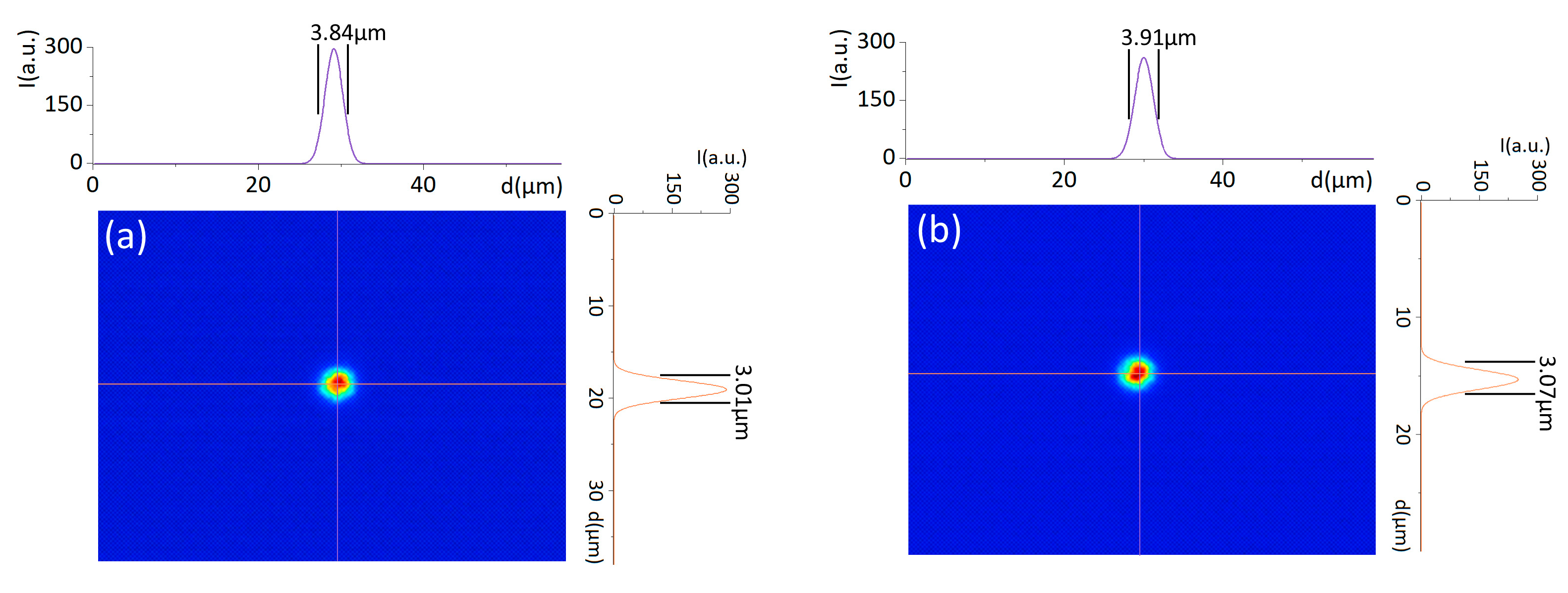
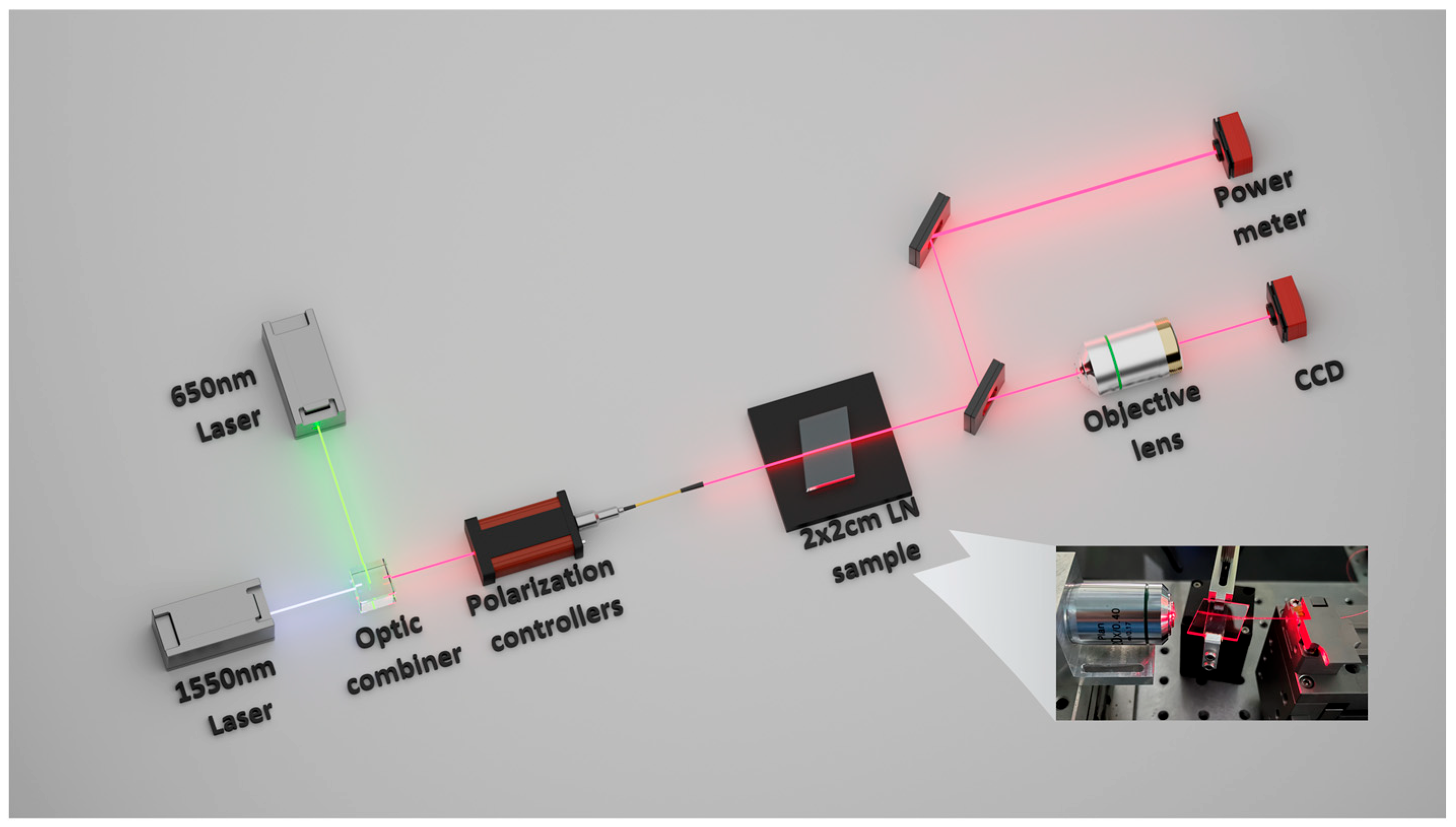
To determine the refractive index distribution of the exchanged planar waveguide profiles, we measured the effective refractive indices of TE modes transmitted through planar waveguides created on X-cut LN samples at a 1550 nm wavelength. This was achieved using a Metricon Model 2010 prism coupler (with a refractive index accuracy of ±0.001), and the profiles’ refractive index distributions were fitted using the IWKB method [25]. To minimize measurement errors caused by the angle between the sample’s optical axis and the vertical direction during refractive index measurements, as well as errors introduced by a limited number of waveguide modes, we ensured that the maximum refractive index of the sample did not surpass the surface refractive index obtained during the longest exchange time. This occurred when the waveguide supported the highest number of optical modes, ensuring a more accurate surface refractive index.
Figure 2 depicts the refractive index profile exhibiting a rapidly varying Fermi distribution when the exchange time is less than 15 h, with the refractive index of the LN substrate at 1550 nm and room temperature marked as n = 2.138. Extending the exchange time results in a refractive index profile displaying a step distribution. The refractive index contrast of the VPE waveguide, ∆n, is 0.082. As per the diffusion coefficient equation [8]:
D t = d 2 4 t ,
where t represents the reaction times, d represents the depth of VPE, the calculated exchange diffusion coefficients for time intervals of 12, 14, 16, and 18 h are 0.067, 0.057, 0.034, and 0.028 μm2/h, respectively. The decreasing trend in diffusion coefficients over time can be attributed to the release of Li+ from the crystals during the reaction, resulting in the dilution of the proton source’s concentration. To assess homogeneity in PE and VPE, we fabricated a proton exchange waveguide within a consistent vessel at 240 °C. During this process, the sample was immersed in a liquid proton source, and we subsequently measured refractive index contrast at various locations on the identical sample piece. Figure 3 illustrates the variation ranges of refractive index contrast for the VPE waveguide (0.0018) and the PE waveguide (0.0166). The difference in fluctuation range for the VPE waveguide closely aligns with the measurement error (±0.001), and the sample variance is 4.5 × 10⁻⁷, signifying minimal data fluctuation. This reveals a narrow refractive index distribution, indicating excellent uniformity in the planar waveguide fabricated by VPE.
XRD was employed to investigate the crystal structure and changes in lattice parameters in the VPE planar waveguide. A crystal plane parallel to the X-cut LN-like surface with Miller indices h = 2, k = 2, and l = 0 (220), corresponding to the Bragg angle ( θ B ) of the substrate at 73.497°, serves as the reference point in Figure 4. Due to the larger lattice parameter of the proton exchange layer compared to the substrate, the peak of the proton-exchange layer is displaced from that of the substrate [26]. This displacement partially indicates the degree of lattice distortion and the eventual development of refractive index contrast. Figure 4 depicts the X-ray rocking curve for the X-cut VPE planar waveguide. For a planar waveguide subjected to stress from the non-protonated substrate, deformations are solely permitted normal to the sample surface [27]. The strain ε 33 , perpendicular to the surface, is directly deducible from the rocking curves. This strain is expressed as ε 33 = Δ θ h k l × c o t θ B , where Δ θ h k l represents the measured angular distance between the substrate peak and the protonated layer peak on the rocking curve relative to the surface plane (hkl), specifically in our case (220). It has been consistently demonstrated that the surface layer consistently exhibits the highest strain value. By analyzing the rocking curves, we ascertain the crystallographic phases and compute the strain values, subsequently comparing them to those documented in the literature [8,27]. The offsets of the 9 h and 18 h curves relative to the substrate peaks in Figure 4 reveal the presence of two peaks in the VPE waveguide, designated as k1 and α. The peak position of the α-phase closely aligns with that of the substrate, and its lattice parameters closely resemble those of the substrate. The peak offsets are −35″ at 9 h and −54″ at 18 h. Furthermore, the −633″ offset in the 9 h and 18 h curves correspond to the k1 phase’s peak, and the intensity of the k1 phase increases with the exchange time, indicating an increase in the crystal layer’s thickness represented by the k1 phase. In prior research, conventional PE exchange often resulted in a mixed phase comprising β, k2, and k1 phases [28]. The lattice constant of the β phase was 0.45% larger than that of normal LN, causing significant lattice distortions that typically necessitated extended annealing periods for recovery [29,30]. When subjected to the VPE process, the X-cut LN waveguide does not show k2, in contrast to the Z-cut LN waveguide [19]. It is important to observe that the signal in the X-cut waveguide between the k1 and α peaks is nearly zero. This suggests a sudden transition between these crystalline phases and a significant mismatch in crystallographic parameters.
The primary focus in optical waveguide devices lies in the propagation characteristics of the waveguides. To address this, we investigated the propagation characteristics of both channel and Y-branch waveguides fabricated using VPE at a wavelength of 1550 nm. Maintaining single-mode propagation at this wavelength requires a reduction in waveguide size due to high refractive index contrast. Using Rsoft simulations, we modeled the refractive index distribution to achieve a single-mode waveguide measuring 3 μm in width. For this purpose, a 100 nm SiO2 mask was used to fabricate 3 μm widths for both the channel waveguide and the Y-branch waveguide via VPE at 300 °C for 12 h. The Y-branch waveguide measures a total length of 2 cm, including a tapered waveguide spanning 200 μm. The width of the tapered waveguide undergoes a transition from 3 μm to 7 μm, and the spacing between the two waveguides at the branch is 1 μm. The two branch waveguides experience separation at a 3° angle. Figure 5 exhibits the microscope image of the Y-branch waveguide, fabricated from a 3-inch X-cut LN wafer. The Y-branch waveguides were arranged in 20 groups equally spaced over a 2 × 2 cm area. The channel waveguide measured a length of 4 cm, and 100 strips were evenly spaced within a 4 × 2 cm area. It is important to note that the narrower opening in the exchange region on the mask leads to a smaller exchange depth in the channel waveguide compared to the planar waveguide. Furthermore, due to non-negligible lateral diffusion during the proton exchange process in the narrower exchange region, the actual width of the waveguide surpasses the mask width.
The exchanged wafer was cut into 4 × 2 cm and 2 × 2 cm diamond-shaped samples with an 80° inclination. These samples were optically polished at both the input and output ends, resulting in a channel waveguide length of 39 ± 0.1 mm and a Y-branch waveguide length of 19 ± 0.1 mm. We measured the near-field transmission modes and transmission losses of the two distinct waveguides. Near-field propagation mode measurements were conducted using a 1550 nm light source, which was coupled to the sample end-face through a fiber optic head made from a bundle of polarization-maintaining fibers. Additionally, a 650 nm visible light source assisted in the testing process. Mode images at the waveguide’s output were captured using an infrared CCD camera from Axiom Optics and a 20× microscope objective. The propagation loss of the single-mode waveguide was assessed via the truncation method. The testing system is depicted in Figure 6.
The insertion loss L O S S i n s e r t of the waveguide can be expressed as:
L O S S i n s e r t = L O S S p r o p + L O S S c o u p l + L O S S r e t u r n ,
where L O S S p r o p represents the propagation loss, L O S S c o u p l represents the coupling loss at the end face, and L O S S r e t u r n is the return loss at the end face. Measuring the insertion loss of different lengths of waveguide, their difference is only determined by the propagation loss difference caused by the length difference. Using the relationship between length difference and insertion loss difference, the propagation loss can be obtained as:
L O S S t r a n = L O S S i n s e r t 1 L O S S i n s e r t 2 Δ L ,
where L O S S i n s e r t 1 and L O S S i n s e r t 2 are the insertion loss measured by two waveguides with different lengths, and Δ L is the length difference between the two waveguides.
We randomly selected 20 out of the 100 channel waveguides and all of the Y-branch waveguides for testing. The results exhibited consistent agreement. The propagation loss and near-field modes of the channel waveguide and Y-branch waveguide are tested as:
a.
The propagation characteristics of the channel waveguide: The pattern image of the channel waveguide with a mask opening of 3 μm, as shown in Figure 7a, was analyzed using FWHM to determine its dimensions in the depth and width directions, which were calculated to be 3.84 ± 0.11 μm and 3.01 ± 0.09 μm, respectively. The propagation loss calculated from the measurements of the five lengths (39 mm, 34 mm, 29 mm, 24 mm, 19 mm) of the channel waveguide was 0.14 ± 0.01 dB/cm, and the polarization extinction ratio was 28.47 dB.
b.
Propagation characteristics of the Y-branch waveguide: Figure 7b shows the mode image of the Y-waveguide with a mask opening of 3 μm. The dimensions in the depth and width directions, calculated using FWHM through multiplicative conversion, are determined to be approximately 3.91 ± 0.15 μm and 3.07 ± 0.1 μm, respectively. The beam-splitting loss is 0.028 dB, the beam-splitting ratio is 1:0.9925, and the polarization extinction ratios of the two ports are 28.21 dB and 28.08 dB, respectively.
Figure 7. Near-field mode images of (a) channel waveguide and (b) Y-branch waveguide at wavelength 1550 nm.
Photonics 10 01390 g007
The planar waveguide, channel waveguide, and Y-branch waveguide were prepared and tested multiple times, all exhibiting good consistency and reproducibility. Additionally, there was no observed degradation in the waveguide performance over three months. This paper compares our enhanced VPE process with schemes from other teams, as demonstrated in Table 2.

4. Discussion

This study successfully performed VPE on lithium niobate wafers, yielding waveguides with a high refractive index contrast (Δn = 0.082) on X-cut LN wafers at 300 °C. Over time, the refractive index distribution shifted from a rapidly varying Fermi distribution to a stepwise distribution. The uniform concentration distribution of H+ in the crucible was ensured due to the large size of the quartz crucible and the gaseous proton source, while a metal basket prevented liquid proton exchange during cooling. The gaseous environment with low H+ concentration around the lithium niobate, along with the superior uniformity in refractive index distribution on the exchanged wafers, is crucial for device stability, particularly in highly symmetric structures like Y-waveguide beam splitters. X-ray diffraction (XRD) analysis of the exchanged planar waveguide revealed an entirely different α phase compared to the substrate crystal structure, along with a high-quality k1 phase. The intensity of the k1 phase increased with exchange time, indicating a thicker proton exchange layer. In contrast to the VPE Z-cut LN waveguide, the X-cut version displayed no k2 phase and exhibited reduced lattice distortion.
Utilizing the optimized process, we fabricated channel waveguides and Y-branch waveguides, achieving a propagation loss (0.14 ± 0.01 dB/cm) comparable to that of the APE process while maintaining a small mode size (3.84 ± 0.11 μm and 3.01 ± 0.09 μm in the depth and width directions, respectively). The Y waveguides prepared through VPE demonstrated an ultra-low beam-splitting loss of 0.028 dB and a highly uniform beam-splitting ratio. All waveguides exhibited polarization extinction ratios surpassing 28 dB, indicating favorable polarization characteristics in VPE-prepared waveguides.

5. Conclusions

In summary, we have demonstrated the successful preparation of waveguides on x-cut lithium niobate using the improved VPE process, achieving index contrast as high as ∆n = 0.08, low propagation losses, small mode sizes channel waveguides, and high-performance Y-branch waveguides. The VPE process is anticipated to enable the realization of electro-optical modulators with substantial modulation depths. The smaller mode-field size can decrease the electrode spacing of the modulator, reduce the drive voltage, enable direct coupling with fibers having small mode-field diameters, and potentially be employed in the future for etching spot-size converters in ridged waveguides. The enhanced VPE technology emerges as a valuable approach to enhance the integration and performance of optical waveguide devices. Looking ahead, there is potential for further in-depth studies on the nonlinear effects, periodic poling, and electro-optical properties of VPE waveguides. The scope of VPE technology can be expanded to lithium niobate thin films, opening avenues for applications such as beam splitters, phase modulators, intensity modulators, and more.

Author Contributions

Conceptualization, S.R.; methodology, S.R.; software, S.R., N.D. and J.L.; validation, S.R., X.W. and P.H.; formal analysis, P.H.; investigation, S.R. and X.W.; resources, S.R. and X.W.; data curation, S.R.; writing—original draft preparation, S.R.; writing—review and editing, P.H.; visualization, P.H.; supervision, P.H.; project administration, S.R. All authors have read and agreed to the published version of the manuscript.

Funding

This research was funded by the Key R&D Program of the Ministry of Science and Technology of China under Project No. SQ2020YFF0421731.

Institutional Review Board Statement

The study did not require ethical approval.

Informed Consent Statement

The study did not involve humans.

Data Availability Statement

Data underlying the results presented in this paper are not publicly available at this time but may be obtained from the authors upon reasonable request.

Conflicts of Interest

All authors have no conflict of interest with “CETC DeQing HuaYing Electronics CO., LTD”.

References

  1. Wang, Z.; Wang, C.; Yu, H. Advances in nonlinear photonic devices based on lithium niobate waveguides. J. Phys. D 2023, 56, 083001. [Google Scholar] [CrossRef]
  2. He, M.; Xu, M.; Ren, Y.; Jian, J.; Ruan, Z.; Xu, Y.; Gao, S.; Sun, S.; Wen, X.; Zhou, L.; et al. High-performance hybrid silicon and lithium niobate Mach–Zehnder modulators for 100 Gbit s−1 and beyond. Nat. Photonics 2019, 13, 359–364. [Google Scholar] [CrossRef]
  3. Wang, C.; Zhang, M.; Chen, X.; Bertrand, M.; Shams-Ansari, A.; Chandrasekhar, S.; Winzer, P.J.; Lončar, M. Integrated lithium niobate electro-optic modulators operating at CMOS-compatible voltages. Nature 2018, 562, 101–104. [Google Scholar] [CrossRef] [PubMed]
  4. Guo, Q.; Sekine, R.; Ledezma, L.; Nehra, R.; Dean, D.J.; Roy, A.; Gray, R.M.; Jahani, S.; Marandi, A. Femtojoule femtosecond all-optical switching in lithium niobate nanophotonics. Nat. Photonics 2022, 16, 625–631. [Google Scholar] [CrossRef]
  5. Liu, H.; Pan, B.; Huang, Y.; He, J.; Zhang, M.; Yu, Z.; Liu, L.; Shi, Y.; Dai, D. Ultra-compact lithium niobate photonic chip for high-capacity and energy-efficient wavelength-division-multiplexing transmitters. Light Sci. Appl. 2023, 4, 1–10. [Google Scholar] [CrossRef]
  6. Chen, Y.; Liu, G.; Zheng, Y.; Geng, F. Periodically poled Ti-diffused near-stoichiometric MgO: LiNbO3 waveguide nonline-ar-optic wavelength converter. Opt. Express 2009, 17, 4834–4841. [Google Scholar] [CrossRef] [PubMed]
  7. Yang, X.; Zhang, Z.; Du, W.; Zhang, Q.; Wong, W.H.; Yu, D.; Pun, E.Y.; Zhang, D. Near-stoichiometric Ti:Sc: LiNbO3 strip waveguide for integrated optics. Opt. Mater. 2016, 6, 2637–2643. [Google Scholar] [CrossRef]
  8. Jackel, J.L.; Rice, C.E.; Veselka, J.J. Proton exchange for high-index waveguides in LiNbO3. Appl. Phys. Lett. 1982, 41, 607–608. [Google Scholar] [CrossRef]
  9. Bortz, M.L.; Fejer, M.M. Annealed proton-exchanged LiNbO3 waveguides. Opt. Lett. 1991, 16, 1844–1846. [Google Scholar] [CrossRef]
  10. Korkishko, Y.N.; Fedorov, V.A.; Laurell, F. The SHG-response of different phases in proton exchanged lithium niobate waveguides. IEEE J. Quantum Electron. 2000, 6, 132–142. [Google Scholar] [CrossRef]
  11. Korkishko, Y.N.; Fedorov, V.A.; Morozova, T.M.; Caccavale, F.; Gonella, F.; Segato, F. Reverse proton exchange for buried waveguides in LiNbO3. J. Opt. Soc. Am. 1998, 15, 1838–1842. [Google Scholar] [CrossRef]
  12. Langrock, C.; Diamanti, E.; Roussev, R.V.; Yamamoto, Y.; Fejer, M.M.; Takesue, H. Highly efficient single-photon detection at communication wavelengths by use of upconversion in reverse-proton-exchanged periodically poled LiNbO3 waveguides. Opt. Lett. 2005, 30, 1725–1727. [Google Scholar] [CrossRef]
  13. Chanvillard, L.; Aschiéri, P.; Baldi, P.; Ostrowsky, D.B.; Micheli, M.D.; Huang, L.; Bamford, D.J. Soft proton exchange on periodically poled LiNbO3: A simple waveguide fabrication process for highly efficient nonlinear interactions. Appl. Phys. Lett. 2000, 76, 1089–1091. [Google Scholar] [CrossRef]
  14. Korkishko, Y.N.; Fedorov, V.A.; Baranov, E.A.; Proyaeva, M.V.; Morozova, T.V.; Caccavale, F.; Segato, F.; Sada, C.; Kostritskii, S.M. Characterization of alpha-phase soft proton-exchanged LiNbO3 optical waveguides. J. Opt. Soc. Am. 2001, 18, 1186–1191. [Google Scholar] [CrossRef] [PubMed]
  15. Rams, J.; Cabrera, J.M. Nonlinear optical efficient LiNbO3 waveguides proton exchanged in benzoic acid vapor: Effect of the vapor pressure. J. Appl. Phys. 1999, 85, 1322–1328. [Google Scholar] [CrossRef]
  16. Ramponi, R.; Osellame, R.; Marangoni, M.; Russo, V. Vapor-phase proton exchange for high quality lithium tantalate waveguides. In Proceedings of the Conference Digest, 2000 Conference on Lasers and Electro-Optics Europe (Cat. No.00TH8505), Nice, France, 10–15 September 2000. [Google Scholar]
  17. Rambu, A.P.; Apetrei, A.M.; Doutre, F.; Tronche, H.; De Micheli, M.; Tascu, S. Analysis of High-Index Contrast Lithium Niobate Waveguides Fabricated by High Vacuum Proton Exchange. J. Light. Technol. 2018, 36, 2675–2684. [Google Scholar] [CrossRef]
  18. Rambu, A.P.; Apetrei, A.M.; Tascu, S. Role of the high vacuum in the precise control of index contrasts and index profiles of LiNbO3 waveguides fabricated by high vacuum proton exchange. Opt. Laser Technol. 2019, 118, 109–114. [Google Scholar] [CrossRef]
  19. Nahm, H.; Park, C. Microscopic structure of hydrogen impurity in LiNbO3. Appl. Phys. Lett. 2001, 78, 3812–3814. [Google Scholar] [CrossRef]
  20. Casey, H.C.; Chen, C.; Zavada, J.M.; Novak, S.W. Analysis of hydrogen diffusion from proton-exchanged layers in LiNbO3. Appl. Phys. Lett. 1993, 63, 718–720. [Google Scholar] [CrossRef]
  21. Rambu, A.P.; Apetrei, A.M.; Doutre, F.; Tronche, H.; Tiron, V.; De Micheli, M.; Tascu, S. Lithium niobate waveguides with high-index contrast and preserved nonlinearity fabricated by a high vacuum vapor-phase proton exchange. Photonics Res. 2020, 8, 8–16. [Google Scholar] [CrossRef]
  22. Rams, J.; Cabrera, J.M. Preparation of proton-exchange LiNbO3 waveguides in benzoic acid vapor. J. Opt. Soc. Am. B 1999, 16, 401–406. [Google Scholar] [CrossRef]
  23. Radojevic, A.M.; Osgood, R.M.; Roy, N.A.; Bakhru, H. Prepatterned optical circuits in thin ion-sliced single-crystal films of LiNbO3. IEEE Photon. 2002, 14, 322–324. [Google Scholar] [CrossRef]
  24. Niu, Y.; Yang, L.; Guo, D.; Chen, Y.; Li, X.; Zhao, G.; Hu, X. Efficient 671 nm red light generation in annealed proton-exchanged periodically poled LiNbO3 waveguides. Chin. Opt. Lett. 2020, 18, 111902. [Google Scholar] [CrossRef]
  25. Mu, X.; Yue, X.; Chen, J.; Wang, J.; Shao, Z. Planar waveguide refractive index distribution functions determined precisely from mode indices. Appl. Opt. 1994, 33, 3227–3230. [Google Scholar] [CrossRef] [PubMed]
  26. Rice, C.E. The structure and properties of Li1-xHxNbO3. J Solid State Chem. 1986, 64, 188–199. [Google Scholar] [CrossRef]
  27. Korkishko, Y.N.; Fedorov, V.A. Structural phase diagram of Hx/Li1-xNbO3 waveguides: The correlation between optical and structural properties. IEEE J. Sel. Top. Quantum Electron. 1996, 2, 187–196. [Google Scholar] [CrossRef]
  28. Fedorov, V.A.; Korkishko, Y.N. Crystal structure and optical properties of proton-exchanged lithium niobate waveguides. In Proceedings of the SPIE’s 1994 International Symposium on Optics, Imaging, and Instrumentation, San Diego, CA, USA, 24–29 July 1994. [Google Scholar]
  29. Ito, K.; Kawamoto, K. Dependence of Lattice Constant Deviation and Refractive Index on Proton Concentration in Proton-Exchanged Optical Waveguides on a Single Crystal of LiNbO3. Jpn. J. Appl. Phys. 1992, 31, 3882–3887. [Google Scholar]
  30. Paz-Pujalt, G.R.; Tuschel, D.D.; Braunstein, G.; Blanton, T.N.; Lee, S.; Salter, L.M. Characterization of proton exchange lithium niobate waveguides. J. Appl. Phys. 1994, 76, 3981–3987. [Google Scholar] [CrossRef]
  31. Peng, Y.; Dai, J.; Li, C. Vapour proton exchange. J. Atmos. Environ. Opt. 2005, 18, 6–9. [Google Scholar]
Figure 1. VPE vessel. The vessel comprises an inner quartz crucible, a metal carrying basket, and a sample holder. The upper and lower sections are laser-fused, and once the desired pressure is attained, the vacuum interface is heated to create an effective seal through the quartz’s collapse.
Photonics 10 01390 g001
Figure 2. Using the IWKB method, we reconstructed refractive index profiles of X-cut LN planar waveguides fabricated via VPE at a wavelength of 1550 nm, employing different reaction times.
Photonics 10 01390 g002
Figure 3. Refractive index contrast histograms of VPE and PE samples are presented. To obtain these planar waveguides, two X-cut LN wafers were subjected to VPE at 300 °C for 30 h and PE at 240 °C for 12 h. The VPE waveguide exhibits a very narrow refractive index contrast distribution, in contrast to the PE waveguide, which displays a large refractive index contrast distribution.
Photonics 10 01390 g003
Figure 4. X-ray rocking curves were generated through reflections from X-cut VPE planar waveguides (220) subjected to thermal exchange at 300 °C for both 9 and 18 h.
Photonics 10 01390 g004
Figure 5. Microscope image of the Y-branch waveguide.
Photonics 10 01390 g005
Figure 6. The schematic and physical representation of near-field mode measurement are illustrated. We utilize lasers with wavelengths of 1550 nm and 650 nm, which are combined and coupled into a single-mode fiber. The polarized light is then output through a polarization controller, coupled into the LN sample via a bias-preserving fiber, and finally guided through a waveguide. The output is received by sub-CCDs and a power meter. The actual test image is displayed in the lower right corner.
Photonics 10 01390 g006
Table 1. Comparison between various optical waveguide fabrication techniques.
Fabrication TechniqueFabrication ConditionIndex ContrastWaveguide WidthNonlinear EffectPolarization Propertyα 3Fabrication Scale
TD [6,7]≥1000 °C, ATM 10.006~0.015~10 μmhigh performancenon0.4~0.7 dB/cmwafer
APE [23,24]150~250 °C, ATM 10.01~0.03~6 μmrequiring annealing for restorationself-polarization0.1~0.2 dB/cmwafer
VPE [21]≥300 °C, HV 2≥0.08≤3 μmhigh performanceself-polarization3.5 dB/cm10 × 15 mm
1 ATM represents standard atmospheric pressure. 2 HV represents high vacuum. 3 α represents propagation loss.
Table 2. Comparison of the improved VPE process in this paper and schemes from other teams.
Reaction VesselTemperatureIndex ContrastRepeatabilitySubstrateα 1
Ampoule [19]350 °C0.10HighZ-cut LN3.5 dB/cm
quartz flask [31]245 °C0.11LowZ-cut LN/
improved quartz crucible in this paper300 °C0.08HighX-cut LN0.14 dB/cm
1 α represents propagation loss.
Disclaimer/Publisher’s Note: The statements, opinions and data contained in all publications are solely those of the individual author(s) and contributor(s) and not of MDPI and/or the editor(s). MDPI and/or the editor(s) disclaim responsibility for any injury to people or property resulting from any ideas, methods, instructions or products referred to in the content.

