Communication

Pulse Width Control Based on Blumlein Pulse Forming Line and SI-GaAs PCSS

Key Laboratory of Ultrafast Photoelectric Technology and Terahertz Science in Shaanxi, Xi’an University of Technology, Xi’an 710048, China
*
Author to whom correspondence should be addressed.
Photonics 2023, 10(2), 156; https://doi.org/10.3390/photonics10020156
Submission received: 25 November 2022 / Revised: 18 January 2023 / Accepted: 31 January 2023 / Published: 2 February 2023

Abstract

:
In this paper, the output electrical pulse width of semi-insulating gallium arsenide photoconductive semiconductor switch (SI-GaAs PCSS) is controlled by means of Blumlein pulse formation line. Under the condition that the bias voltage is 28 kV and the laser pulse width is 9.5 ns, the electric pulse width obtained by using high-power pulse system transmission is 10 ns and the output voltage is 23 kV. Based on the Blumlein pulse formation line theory, the output pulse width and transient impedance are analyzed. The results show that the holding time of carriers avalanche multiplication can be controlled.

1. Introduction

The core of pulse power technology is the compression of energy during the transfer process, then the release of the energy in a short time through switching technology. With the development of pulsed power technology applications, high-power narrow pulses are of increasing attention, especially in ultra-wideband radar, biomedical and dielectric wall accelerator are in demand. The key technology of pulse power is switching technology, and switching devices is the core devices in the whole pulse power technology system. It plays a key role in the whole system, and the parameters of switching devices determine the stability of the whole system performance [1,2]. Metallic Oxide Semiconductor Field Effect Transistor (MOSFET) have the fastest response and low switching losses among power electronics devices and are widely used in high-frequency devices with frequencies up to MHz level, but MOSFET have small current capacity, low withstand voltage, and the power of a single tube generally does not exceed 10 kW. At voltages above 1000 V, IGBT switching losses are 1/10 that of Giant Transistors (GTR) and comparable to MOSFET when compared to power MOSFET and GTR. As a result, they have difficulty combining high repetition frequencies and power capacities, such as kilowatt-scale silicon IGBT with maximum operating frequencies in the 100 kHz range. PCSS have excellent characteristics in terms of both bandwidth and power, and are particularly prominent in the field of high-power electromagnetic pulse generation. Compared with other types of switches, PCSS have the advantages of simple structure, fast response, litter jitter and low parasitic inductance [3,4,5]. Furthermore, it is widely used in the fields of ultra-high speed electronics, solid-state pulse power sources, high speed photodetectors, THz radiation sources, etc. It is a semiconductor optoelectronic device with rapid development in recent years [6,7,8]. Due to its excellent performance, PCSS is considered to be a power switching device with great potential for future development. However, the width of the switch output electrical pulse is usually much wider than the trigger optical source. So the switch is usually triggered by a shorter laser, such as the fs laser, which is not only expensive but also bulky for the commercialization of the system. Therefore, finding a way to break the limitation of laser pulse width has become an important research direction.
In 1975, D.H. Auston of Bell Laboratories produced the first silicon optoelectronic semiconductor photoconductor switch on a microstrip line. The transmission efficiency of the switch circuit was about 50%, and published the relevant article about the photoconductive switch to generatein the kV and ns magnitudes electrical pulses by ps laser pulse triggering [9]. In 1977, C.H. Lee et al. first developed GaAs PCSS and operated it at a repetitive frequency of 1 GHz, pointing out that GaAs material has more performance advantages than silicon material in making photoconductive switches [10]. In 2010, Merla designed a new ns-level pulse source consisting of a photoconductive switch and a microstrip line that can withstand a voltage of 4 kV. The matching resistance is 10 Ω and a pulse width of less than 5 ns. It is used in biological experimental research [11]. At present, the width of the output pulse can be controlled by adjusting the energy-storage capacitance [12]. However, because of the uncertainty of discharge rate and discharge efficiency, it is difficult to accurately control the output pulse width.
In this paper, a high-power pulse system with Blumlein pulse forming line structure is designed. Its main components are Blumlein pulse forming line, SI-GaAs PCSS and solid-state laser. The Blumlein pulse formation line can be designed with pulse width and impedance according to actual requirements, and when it is combined with SI-GaAs PCSS, it can effectively control the width of the output electrical pulse.The transient impedance of SI-GaAs PCSS is also analyzed based on the basic theory of pulse Blumlein pulse forming line.

2. Experimental Setup
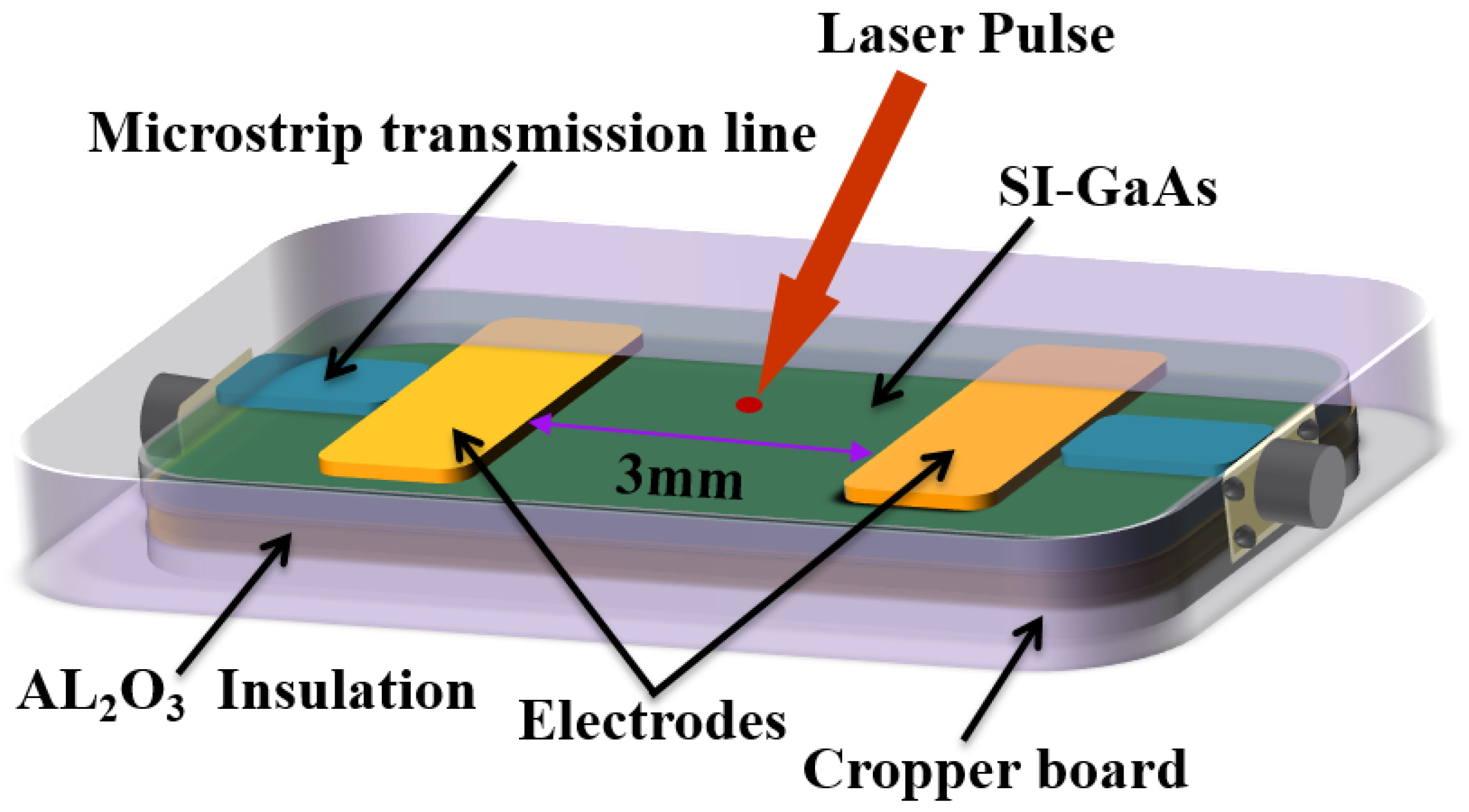
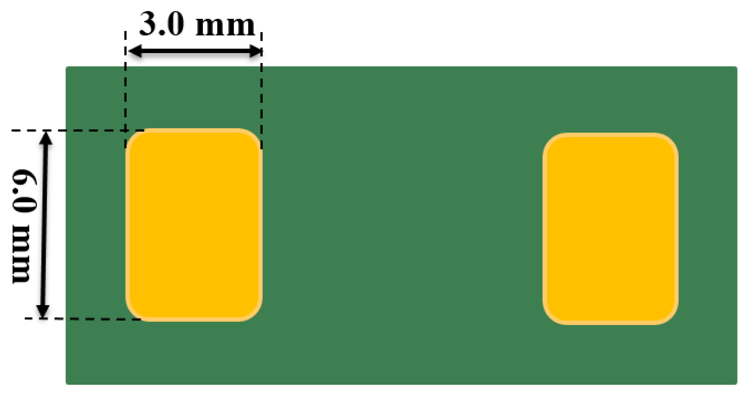
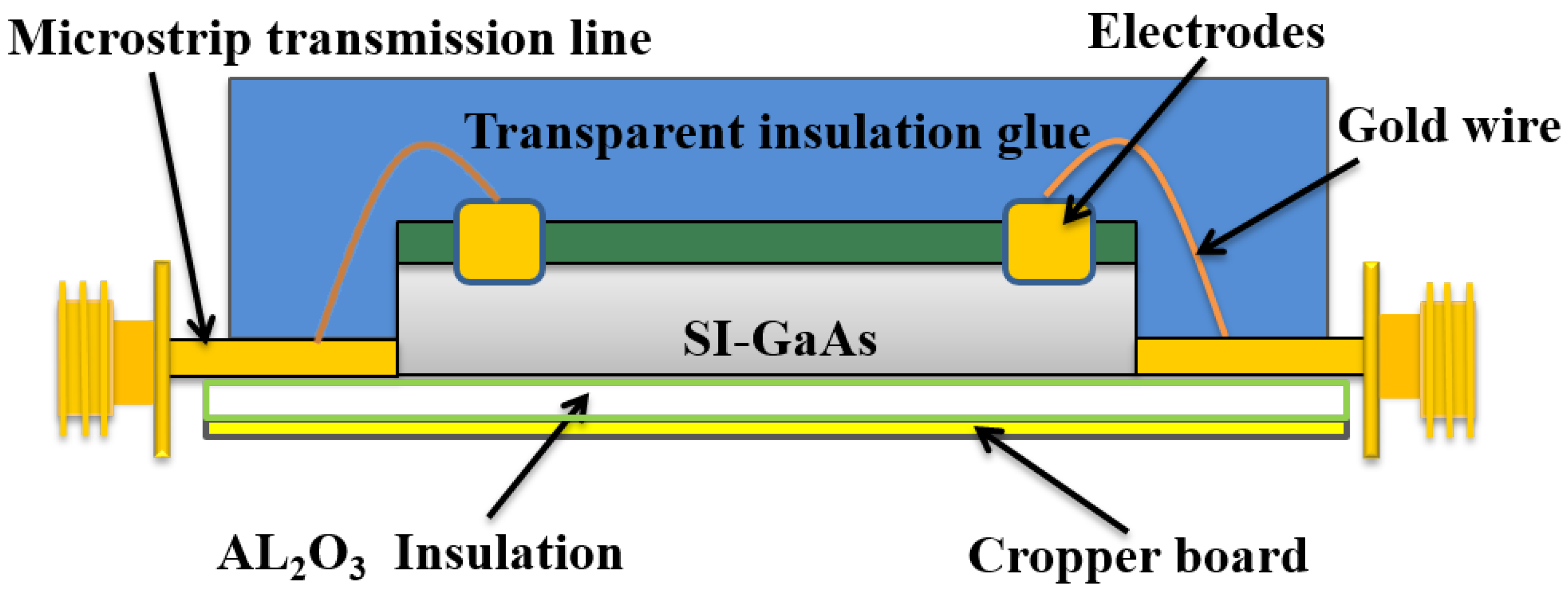
2.1. SI-GaAs PCSS

On the basis of existing processes and experiments, GaAs materials with EL2 or Cr compensation and Si injection are selected for the experiment. The dark-state resistivity of the lateral SI-GaAs PCSS is greater than 5 × 10 7 Ω ·cm, and its electron mobility is greater than 5000 cm 2 /(V·s). The electrodes gap of SI-GaAs PCSS is 3 mm, and the overall size is 10.0 mm (width) × 15.0 mm (length) × 0.6 mm (thickness), as shown in Figure 1. The electrodes adopts Au/Ge/Ni/Au, the size of each electrode is 6.0 mm × 3.0 mm, the electrodes were optimized with a fillet radius of 1.1 mm, as shown in Figure 2. This structure is beneficial to improve the compressive strength of SI-GaAs PCSS. In order to improve the insulation strength, three-layer insulation was used in the experiment. In addition to the Si 3 N 4 passivation layer of the SI-GaAs PCSS, the switch was encapsulated with transparent insulation glue and then placed in liquid insulating oil, as shown in Figure 3.

2.2. Test Circuit

The trigger optical source is provided by a Nd:YAG solid-state laser with a wavelength of 1064 nm, a pulse width of 9.5 ns and an energy of 78 mJ. In the experiment, a high-power pulse system with a Blumlein pulse forming line structure is used. Blumlein pulse forming line is made of ceramic medium with silver electrode printed on both sides. Furthermore, the size of ceramic medium is 300.0 mm × 30.0 mm, silver electrode size is 280.0 mm × 4.0 mm, as shown in Figure 4. The Blumlein pulse forming line is connected with the circuit through the coaxial transmission line, and the load resistance R L in the test circuit is 150 Ω . When the optical pulse triggers the SI-GaAs PCSS, the output electrical pulse signal passes through the coaxial line and the 60-dB attenuator, and finally enters the oscilloscope with the bandwidth of 1GHz (LeCroy HDO4104). The test circuit is shown in Figure 5.

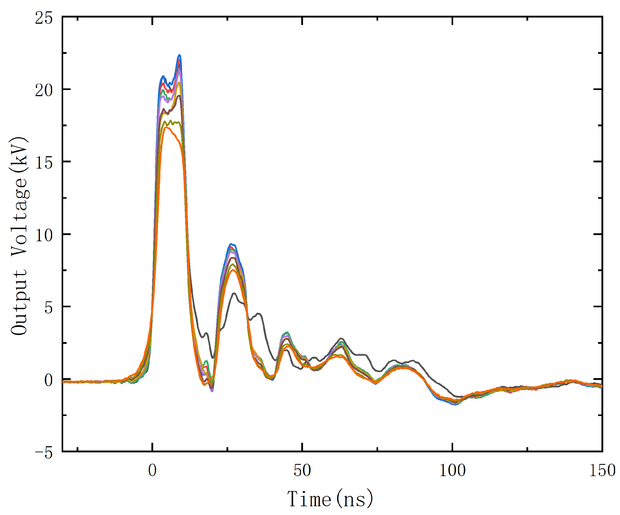
3. Results and Discussion

The SI-GaAs PCSS is triggered at a bias voltage is 28 kV and the trigger optical energy is 78 mJ, the PCSS enters the nonlinear operating mode. The main feature of SI-GaAs PCSS into nonlinear mode of operation is the multiplication rate of carriers. The carrier multiplication rate is calculated by using the ratio of absorbed photons to output electron-hole pairs in the nonlinear mode of operation of the PCSS, which reflects the depth of the nonlinear mode of the PCSS. In the paper, the multiplication rate of carriers is 58.2 for a bias voltage of 28 kV. Figure 6 shows the output electrical pulse transmitted through the Blumlein pulse formation line.
The width of the electrical pulse is 10 ns, the rise time is 2 ns and the output voltage is 23 kV. The width of the output electrical pulse is wider than the trigger optical pulse. In the pursuit of system optimization, the lower time jitter of SI-GaAs PCSS plays a critical role in enhancing the stability and the capacity of any system. The jitter value can describe avalanche stability quantitatively. The 10 repetitive output current waveforms are presented in Figure 7. When the bias voltage is 28 kV, the jitter value of SI-GaAs PCSS is 47.9 ps.
The transmission efficiency of waveform peak voltage is 82.14%. Since the SI-GaAs PCSS ON-state resistance is a time-dependent quantity during the process of switch conduction. Furthermore, the peak of the output electrical pulse waveform is the minimum value of the switch ON-state resistance. The smaller the SI-GaAs PCSS ON-state resistance R t , the higher the voltage transfer efficiency after the switch circuit is turned on. The triggering process of the SI-GaAs PCSS is accompanied by current ablation of the electrodes, and the PCSS was eventually damaged due to electrodes breakage. 3-mm electrodes gap can withstand 4888 pulses triggered by Nd:YAG laser. The Lifetime of the SI-GaAs PCSS is 4888 pulses. The Blumlein pulse forming line has the transmission characteristics to realize the output of electrical pulses with different pulse widths. Therefore, according to the basic theory of Blumlein pulse formation line, the output pulse width and impedance of its main parameters are analyzed.
According to the basic theory of Blumlein pulse formation line, the output pulse width can be expressed as,
τ = 2 l ε r μ r c
Here, l is the length of Blumlein pulse forming line, c = 3 × 10 8 m/s is the speed of optical propagation, ε r = 60 is the relative permittivity of the dielectric, μ r = 1 is the relative permeability of the dielectric [13,14,15]. It can be seen from Equation (1) that the pulse width of output voltage mainly depends on the length of Blumlein pulse forming line. Moreover, increasing the dielectric constant and permeability is helpful to reduce the length of Blumlein pulse formation line. At present, the width of the output electric pulse can also be controlled by adjusting the energy-storage capacitance, but the energy-storage capacitance has problems such as discharge rate and discharge efficiency. Therefore, it is more accurately to adjust the output electric pulse width through the Blumlein pulse forming line.
The transient impedance is also one of the most important parameters of Blumlein pulse forming line. Theoretically, the impedance Z s of Blumlein pulse forming line can be expressed as,
Z s = R + j ω L G + j ω C
The transient impedance of Blumlein pulse forming line is related to its resistance, conductance, inductance and capacitance per unit length. For uniform lossless transmission lines, R = 0 , G = 0 .
Z s = L C
In practical application, the transient impedance of Blumlein pulse formation line can be expressed as,
Z s = μ 0 μ r ε 0 ε r d d + W = 377 d d + W μ r ε r
Here, d = 4 mm is the thickness of Blumlein pulse forming line, W is the electrode width of Blumlein pulse forming line, ε 0 = 8.85 × 10 12 F/m is the permittivity of vacuum, μ 0 = 4 π × 10 7 H/m is the permeability of vacuum [16]. The calculated characteristic impedance of Blumlein pulse forming line is 49 Ω .
When the SI-GaAs PCSS is triggered, part of the signal in the voltage wave that passes through the Blumlein pulse forming line is reflected and part of the signal is transmitted. The integrity of the signal is damaged. In the process of signal transmission, part of the electrical signal will be reflected due to the influence of instantaneous impedance response. The unreflected signal will continue to propagate, but the amplitude and waveform will be changed. According to the definition of transmission line reflection coefficient deduced that,
ρ = Z 0 Z s Z 0 + Z s = V r V i
where, ρ is the reflection coefficient, V i is the incident voltage, V r is the reflected voltage, and Z 0 is the impedance of SI-GaAs PCSS.
After the SI-GaAs PCSS enters the nonlinear operating mode, the ON-state resistance of the SI-GaAs PCSS decreases sharply to the ohmic or subohmic order due to the avalanche multiplication effect of carriers [17]. At this time, the switching impedance Z 0 is smaller than Z s , the reflection coefficient ρ < 0 and the reflected voltage V r is negative, according to Equation (5). As the switch impedance Z 0 decrease, the bias voltage will keep decreasing under the action of reflected voltage wave with a negative reflection coefficient. When the bias voltage is less than the threshold voltage, the photon-activated charge domain (PACD) will be quenched and the switch returns to the off state. Compared with low bias voltage, carriers avalanche multiplication effect under high bias voltage is very strong, so the switching impedance Z 0 changes very quickly. In the nonlinear operating mode, when the electric pulse rises to a certain value, if the value of the bias voltage is just equal to the threshold voltage, the PACD will be quenched rapidly. So the electric pulse will fall rapidly before the rise is completed, and an ultra-short pulse will be obtained. From the analysis, it can be concluded that SI-GaAs PCSS under the nonlinear quenching mode, the rapid formation and quenching process of PACD leads to the output of ultra-fast electrical pulses.

4. Conclusions

In this paper, the Blumlein pulse forming line is combined with the traditional test circuit of SI-GaAs PCSS, and the output pulse width is 10 ns under the condition of 28 kV bias voltage. By the energy-storage means of Blumlein pulse forming line, the holding time of carrier avalanche multiplication is controlled. The transient impedance of Blumlein pulse forming line during the transmission is analyzed. It was seen that the negative reflected voltage wave in the nonlinear operating mode is the reason for the continuous decrease in bias voltage. The rapid decrease in the impedance of SI-GaAs PCSS causes the PACD to quench, and the switch quickly returns to the off state, thus realizing the output of ultra-short electrical pulses.

Author Contributions

W.S.; methodology, W.S. and M.W.; software, W.S., M.W. and C.M.; validation, W.S., M.W. and C.M.; formal analysis, M.W., and Z.C.; investigation, Z.C. and H.L.; resources, W.S., C.M. and M.W.; data curation, W.S. and M.W.; writing—original draft preparation, W.S. and M.W.; writing—review and editing, W.S.; visualization, W.S. and M.W.; supervision, W.S., M.W. and C.M.; project administration, W.S.; funding acquisition, W.S. All authors have read and agreed to the published version of the manuscript.

Funding

This research was funded by the National Key Research and Development Program of China (Grant No. 2017YFA0701005), the National Natural Science Foundational of China (Grant No. 51807161) and the Scientific research project of Shaanxi Provincial Department of Education (Grant No. 21JK0588).

Institutional Review Board Statement

Not applicable.

Informed Consent Statement

Informed consent was obtained from all subjects involved in the study.

Data Availability Statement

Not applicable.

Conflicts of Interest

The authors declare no conflict of interest.

References

  1. Ajram, S.; Salmer, G. Ultrahigh frequency DC-to-DC converters using GaAs power switches. IEEE Trans. Power Electron. 2001, 16, 594–602. [Google Scholar] [CrossRef]
  2. Chang, C.; Liu, G.; Tang, C.; Chen, C.; Fang, J. Review of recent theories and experiments for improving high-power microwave window breakdown thresholds. Phys. Plasmas 2011, 18, 055702. [Google Scholar] [CrossRef]
  3. Vergne, B.; Couderc, V.; Barthélémy, A.; Gontier, D.; Lalande, M.; Bertrand, V. High-voltage rectifier diodes used as photoconductive device for microwave pulse generation. IEEE Trans. Plasma Sci. 2006, 34, 1806–1813. [Google Scholar] [CrossRef]
  4. Wang, W.; Xia, L.; Chen, Y.; Liu, Y.; Yang, C.; Ye, M.; Deng, J. Research on synchronization of 15 parallel high gain photoconductive semiconductor switches triggered by high power pulse laser diodes. Appl. Phys. Lett. 2015, 106, 022108. [Google Scholar] [CrossRef]
  5. Shi, W.; Zhang, L.; Gui, H.; Hou, L.; Xu, M.; Qu, G. Accurate measurement of the jitter time of GaAs photoconductive semiconductor switches triggered by a one-to-two optical fiber. Appl. Phys. Lett. 2013, 102, 154106. [Google Scholar] [CrossRef]
  6. Schoenberg, J.S.; Burger, J.W.; Tyo, J.S.; Abdalla, M.D.; Skipper, M.C.; Buchwald, W.R. Ultra-wideband source using gallium arsenide photoconductive semiconductor switches. IEEE Trans. Plasma Sci. 1997, 25, 327–334. [Google Scholar] [CrossRef]
  7. Nunnally, W.C. High-power microwave generation using optically activated semiconductor switches. IEEE Trans. Electron Devices 1990, 37, 2439–2448. [Google Scholar] [CrossRef]
  8. Islam, N.; Schamiloglu, E.; Fleddermann, C.; Schoenberg, J.; Joshi, R. Analysis of high voltage operation of gallium arsenide photoconductive switches used in high power applications. J. Appl. Phys. 1999, 86, 1754–1758. [Google Scholar] [CrossRef]
  9. Auston, D.H. Picosecond optoelectronic switching and gating in silicon. Appl. Phys. Lett. 1975, 26, 101–103. [Google Scholar] [CrossRef]
  10. Lee, C.H. Picosecond optoelectronic switching in GaAs. Appl. Phys. Lett. 1977, 30, 84–86. [Google Scholar] [CrossRef]
  11. Merla, C.; El Amari, S.; Kenaan, M.; Liberti, M.; Apollonio, F.; Arnaud-Cormos, D.; Couderc, V.; Leveque, P. A 10-Ω High-Voltage Nanosecond Pulse Generator. IEEE Trans. Microw. Theory Tech. 2010, 58, 4079–4085. [Google Scholar] [CrossRef]
  12. Shi, W.; Wu, M.; Ma, C.; Chen, Z. Pulse width Control of Nonlinear GaAs Photoconductive Semiconductor Switch. IEEE Trans. Electron. Devices 2022, 69, 4396–4400. [Google Scholar] [CrossRef]
  13. Mi, Y.; Zhang, Y.; Wan, J.; Yao, C.; Li, C. Nanosecond pulse generator based on an unbalanced blumlein-type multilayered microstrip transmission line and solid-state switches. IEEE Trans. Plasma Sci. 2016, 44, 795–802. [Google Scholar] [CrossRef]
  14. Wang, L.; Liu, J.; Zhang, Q. Effect of different environmental dielectrics on the pulse-forming characteristics of solid-state meander pulse-forming line. IEEE Trans. Plasma Sci. 2016, 44, 821–828. [Google Scholar] [CrossRef]
  15. Geng, Y.; Zou, H.; Li, C.; Sun, J.; Wang, H.; Wang, P. Short pulse generation with on-chip pulse-forming lines. IEEE Trans. Very Large Scale Integr. VLSI Syst. 2011, 20, 1553–1564. [Google Scholar] [CrossRef]
  16. Ma, C.; Yang, L.; Wang, S.; Ji, Y.; Zhang, L.; Shi, W. Study of the lifetime of high-power GaAs PCSSs under different energy storage modes. IEEE Trans. Power Electron. 2016, 32, 4644–4651. [Google Scholar] [CrossRef]
  17. Xiao, L.; Hu, X.; Chen, X.; Peng, Y.; Yang, X.; Xu, X. Effect of periodic array on the on-state resistances of GaAs photoconductive semiconductor switch based on total reflection theory. AIP Adv. 2017, 7, 065119. [Google Scholar] [CrossRef] [Green Version]
Figure 1. Schematic diagram of SI-GaAs PCSS.
Photonics 10 00156 g001
Figure 2. Top view of SI-GaAs PCSS electrodes.
Photonics 10 00156 g002
Figure 3. Cross-section of the SI-GaAs PCSS.
Photonics 10 00156 g003
Figure 4. Schematic diagram of Blumlein pulse forming line.
Photonics 10 00156 g004
Figure 5. Schematic diagram of test circuit.
Photonics 10 00156 g005
Figure 6. Output pulse waveform of SI-GaAs PCSS with 3 mm electrodes gap.
Photonics 10 00156 g006
Figure 7. Ten repetitive output waveforms of the SI-GaAs PCSS biased at 28 kV.
Photonics 10 00156 g007
Disclaimer/Publisher’s Note: The statements, opinions and data contained in all publications are solely those of the individual author(s) and contributor(s) and not of MDPI and/or the editor(s). MDPI and/or the editor(s) disclaim responsibility for any injury to people or property resulting from any ideas, methods, instructions or products referred to in the content.

