Parallelized and Cascadable Optical Logic Operations by Few-Layer Diffractive Optical Neural Network

Abstract
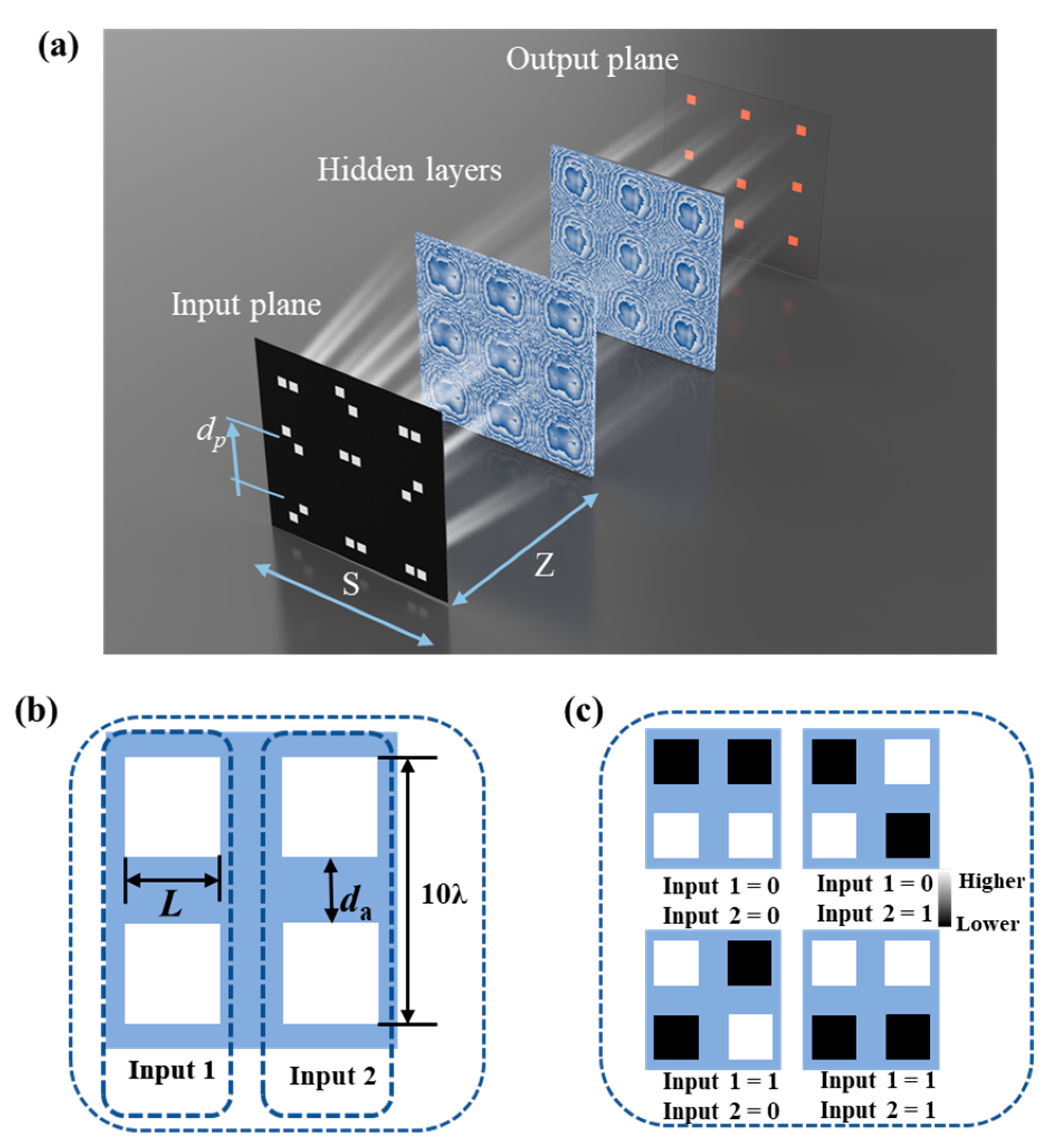
:1. Introduction
2. System and Method
3. Results
3.1. 2-Hidden-Layer DONN for Various Logic Operations
3.2. Effect of Pixel–Pixel Distance and Densely Integrated Logic Pixels
3.3. 16-Bit NAND Gate Operation and Transformation to NOR Gate
3.4. Cascaded DONNs for AND Logic Operation
4. Discussion
5. Conclusions
Author Contributions
Funding
Institutional Review Board Statement
Informed Consent Statement
Data Availability Statement
Conflicts of Interest
References
- Shen, Y.; Harris, N.C.; Skirlo, S.; Prabhu, M.; Baehr-Jones, T.; Hochberg, M.; Sun, X.; Zhao, S.; Larochelle, H.; Englund, D.; et al. Deep Learning with Coherent Nanophotonic Circuits. Nat. Photonics 2017, 11, 441–446. [Google Scholar]
- Zhu, H.H.; Zou, J.; Zhang, H.; Shi, Y.Z.; Luo, S.B.; Wang, N.; Cai, H.; Wan, L.X.; Wang, B.; Jiang, X.D.; et al. Space-Efficient Optical Computing with an Integrated Chip Diffractive Neural Network. Nat. Commun. 2022, 13, 1044. [Google Scholar] [PubMed]
- Harris, N.C.; Carolan, J.; Bunandar, D.; Prabhu, M.; Hochberg, M.; Baehr-Jones, T.; Fanto, M.L.; Smith, A.M.; Tison, C.C.; Alsing, P.M.; et al. Linear Programmable Nanophotonic Processors. Optica 2018, 5, 1623–1631. [Google Scholar]
- Lin, X.; Rivenson, Y.; Yardimci, N.T.; Veli, M.; Luo, Y.; Jarrahi, M.; Ozcan, A. All-Optical Machine Learning Using Diffractive Deep Neural Networks. Science 2018, 361, 1004–1008. [Google Scholar] [PubMed]
- Zheng, M.; Shi, L.; Zi, J. Optimize Performance of a Diffractive Neural Network by Controlling the Fresnel Number. Photonics Res. 2022, 10, 2667–2676. [Google Scholar]
- Luo, X.; Hu, Y.; Ou, X.; Li, X.; Lai, J.; Liu, N.; Cheng, X.; Pan, A.; Duan, H. Metasurface-Enabled on-Chip Multiplexed Diffractive Neural Networks in the Visible. Light Sci. Appl. 2022, 11, 158. [Google Scholar]
- Goi, E.; Chen, X.; Zhang, Q.; Cumming, B.P.; Schoenhardt, S.; Luan, H.; Gu, M. Nanoprinted High-Neuron-Density Optical Linear Perceptrons Performing near-Infrared Inference on a CMOS Chip. Light Sci. Appl. 2021, 10, 40. [Google Scholar] [PubMed]
- Mengu, D.; Ozcan, A. All-Optical Phase Recovery: Diffractive Computing for Quantitative Phase Imaging. Adv. Opt. Mater. 2022, 10, 2200281. [Google Scholar]
- Luo, Y.; Mengu, D.; Ozcan, A. Cascadable All-Optical NAND Gates Using Diffractive Networks. Sci. Rep. 2022, 12, 7121. [Google Scholar] [PubMed]
- Sakib Rahman, M.S.; Ozcan, A. Computer-Free, All-Optical Reconstruction of Holograms Using Diffractive Networks. ACS Photonics 2021, 8, 3375–3384. [Google Scholar] [CrossRef]
- Yan, T.; Wu, J.; Zhou, T.; Xie, H.; Xu, F.; Fan, J.; Fang, L.; Lin, X.; Dai, Q. Fourier-Space Diffractive Deep Neural Network. Phys. Rev. Lett. 2019, 123, 023901. [Google Scholar] [CrossRef] [PubMed]
- Huang, Z.; Wang, P.; Liu, J.; Xiong, W.; He, Y.; Xiao, J.; Ye, H.; Li, Y.; Chen, S.; Fan, D. All-Optical Signal Processing of Vortex Beams with Diffractive Deep Neural Networks. Phys. Rev. Appl. 2021, 15, 014037. [Google Scholar] [CrossRef]
- Liu, Z.; Gao, S.; Lai, Z.; Li, Y.; Ao, Z.; Li, J.; Tu, J.; Wu, Y.; Liu, W.; Li, Z. Broadband, Low-Crosstalk, and Massive-Channels OAM Modes De/Multiplexing Based on Optical Diffraction Neural Network. Laser Photonics Rev. 2200536. [CrossRef]
- Wang, H.; Zhan, Z.; Hu, F.; Meng, Y.; Liu, Z.; Fu, X.; Liu, Q. Intelligent Optoelectronic Processor for Orbital Angular Momentum Spectrum Measurement. PhotoniX 2023, 4, 9. [Google Scholar] [CrossRef]
- Duan, Z.; Chen, H.; Lin, X. Optical Multi-Task Learning Using Multi-Wavelength Diffractive Deep Neural Networks. Nanophotonics 2023, 12, 893–903. [Google Scholar] [CrossRef]
- Fu, T.; Zang, Y.; Huang, Y.; Du, Z.; Huang, H.; Hu, C.; Chen, M.; Yang, S.; Chen, H. Photonic Machine Learning with On-Chip Diffractive Optics. Nat. Commun. 2023, 14, 70. [Google Scholar] [CrossRef]
- Wang, Z.; Chang, L.; Wang, F.; Li, T.; Gu, T. Integrated Photonic Metasystem for Image Classifications at Telecommunication Wavelength. Nat. Commun. 2022, 13, 2131. [Google Scholar] [CrossRef] [PubMed]
- Tang, C.; Dou, X.; Lin, Y.; Yin, H.; Wu, B.; Zhao, Q. Design of All-Optical Logic Gates Avoiding External Phase Shifters in a Two-Dimensional Photonic Crystal Based on Multi-Mode Interference for BPSK Signals. Opt. Commun. 2014, 316, 49–55. [Google Scholar] [CrossRef]
- Mohebzadeh-Bahabady, A.; Olyaee, S. Proposal of a Cascade Photonic Crystal XOR Logic Gate for Optical Integrated Circuits with Investigation of Fabrication Error and Optical Power Changes. Photonics 2021, 8, 392. [Google Scholar] [CrossRef]
- El Haffar, R.; Mahboub, O.; Farkhsi, A.; Figuigue, M. All-Optical Logic Gates Using a Plasmonic MIM Waveguide and Elliptical Ring Resonator. Plasmonics 2022, 17, 831–842. [Google Scholar] [CrossRef]
- He, L.; Zhang, F.; Zhang, H.; Kong, L.-J.; Zhang, W.; Xu, X.; Zhang, X. Topology-Optimized Ultracompact All-Optical Logic Devices on Silicon Photonic Platforms. ACS Photonics 2022, 9, 597–604. [Google Scholar] [CrossRef]
- Neşeli, B.; Yilmaz, Y.A.; Kurt, H.; Turduev, M. Inverse Design of Ultra-Compact Photonic Gates for All-Optical Logic Operations. J. Phys. Appl. Phys. 2022, 55, 215107. [Google Scholar] [CrossRef]
- Chen, T.; Dang, Z.; Ding, Z.; Zhang, Z. Programmable Parallel Optical Logic Gates on a Multimode Waveguide Engine. Photonics 2022, 9, 736. [Google Scholar] [CrossRef]
- Huang, Y.; Xiao, T.; Chen, S.; Xie, Z.; Zheng, J.; Zhu, J.; Su, Y.; Chen, W.; Liu, K.; Tang, M.; et al. All-Optical Controlled-NOT Logic Gate Achieving Directional Asymmetric Transmission Based on Metasurface Doublet. Opto-Electron. Adv. 2023, 6, 220073. [Google Scholar] [CrossRef]
- Jiao, S.; Feng, J.; Zhang, L.; Wu, D.; Shen, Y. Optical Logic Gate Operations with Single-Pixel Imaging. IEEE J. Sel. Top. Quantum Electron. 2023, 29, 1–8. [Google Scholar] [CrossRef]
- Mukherjee, K.; Raja, A.; Maji, K. All-Optical Logic Gate NAND Using Semiconductor Optical Amplifiers with Simulation. J. Opt. 2019, 48, 357–364. [Google Scholar] [CrossRef]
- Miller, D.A.B. Are Optical Transistors the Logical next Step? Nat. Photonics 2010, 4, 3–5. [Google Scholar] [CrossRef]
- Qian, C.; Lin, X.; Lin, X.; Xu, J.; Sun, Y.; Li, E.; Zhang, B.; Chen, H. Performing Optical Logic Operations by a Diffractive Neural Network. Light Sci. Appl. 2020, 9, 59. [Google Scholar] [CrossRef] [PubMed]
- Wang, P.; Xiong, W.; Huang, Z.; He, Y.; Xie, Z.; Liu, J.; Ye, H.; Li, Y.; Fan, D.; Chen, S. Orbital Angular Momentum Mode Logical Operation Using Optical Diffractive Neural Network. Photonics Res. 2021, 9, 2116–2124. [Google Scholar] [CrossRef]
- Zarei, S.; Khavasi, A. Realization of Optical Logic Gates Using On-Chip Diffractive Optical Neural Networks. Sci. Rep. 2022, 12, 15747. [Google Scholar] [CrossRef] [PubMed]
- Zhao, Z.; Zhao, Z.; Wang, Y.; Ding, X.; Ding, X.; Li, H.; Li, H.; Fu, J.; Zhang, K.; Zhang, K.; et al. Compact Logic Operator Utilizing a Single-Layer Metasurface. Photonics Res. 2022, 10, 316–322. [Google Scholar] [CrossRef]
- Mengu, D.; Zhao, Y.; Yardimci, N.T.; Rivenson, Y.; Jarrahi, M.; Ozcan, A. Misalignment Resilient Diffractive Optical Networks. Nanophotonics 2020, 9, 4207–4219. [Google Scholar] [CrossRef]


| Logic-Pixel Index | Input 1 | Input 2 | Expected Output | Output Light Intensity | Correctness Check |
|---|---|---|---|---|---|
| (1, 1) | 1 | 1 | 0 | (3.75, 75.66) | √ |
| (1, 2) | 0 | 1 | 1 | (47.98, 20.82) | √ |
| (1, 3) | 0 | 1 | 1 | (49.64, 20.54) | √ |
| (1, 4) | 1 | 0 | 1 | (50.89, 19.23) | √ |
| (2, 1) | 1 | 0 | 1 | (50.03, 21.13) | √ |
| (2, 2) | 1 | 0 | 1 | (49.27, 20.42) | √ |
| (2, 3) | 1 | 0 | 1 | (48.69, 21.48) | √ |
| (2, 4) | 1 | 0 | 1 | (50.39, 18.90) | √ |
| (3, 1) | 1 | 0 | 1 | (50.58, 22.36) | √ |
| (3, 2) | 1 | 1 | 0 | (4.08, 77.43) | √ |
| (3, 3) | 1 | 1 | 0 | (4.24, 79.30) | √ |
| (3, 4) | 0 | 1 | 1 | (49.43, 19.82) | √ |
| (4, 1) | 1 | 1 | 0 | (3.75, 75.49) | √ |
| (4, 2) | 0 | 1 | 1 | (48.65, 20.99) | √ |
| (4, 3) | 1 | 1 | 0 | (3.76, 73.37) | √ |
| (4, 4) | 0 | 0 | 1 | (78.85, 1.12) | √ |
| Logic-Pixel Index | Input 1 | Input 2 | Expected Output | Output Light Intensity | Correctness Check |
|---|---|---|---|---|---|
| (1, 1) | 1 | 0 | 0 | (19.13, 52.4) | √ |
| (1, 2) | 0 | 0 | 1 | (72.56, 3.892) | √ |
| (1, 3) | 1 | 1 | 0 | (1.095, 78.6) | √ |
| (1, 4) | 0 | 1 | 0 | (17.39, 50.0) | √ |
| (2, 1) | 0 | 0 | 1 | (77.92, 3.837) | √ |
| (2, 2) | 0 | 0 | 1 | (78.85, 4.345) | √ |
| (2, 3) | 1 | 0 | 0 | (20.98, 47.3) | √ |
| (2, 4) | 0 | 1 | 0 | (19.82, 8.529) | √ |
| (3, 1) | 1 | 1 | 0 | (1.465, 77.6) | √ |
| (3, 2) | 1 | 1 | 0 | (21.13, 49.23) | √ |
| (3, 3) | 0 | 0 | 1 | (73.56, 4.645) | √ |
| (3, 4) | 1 | 1 | 0 | (20.71, 48.6) | √ |
| (4, 1) | 0 | 1 | 0 | (17.64, 50.5) | √ |
| (4, 2) | 1 | 1 | 0 | (1.769, 75.9) | √ |
| (4, 3) | 1 | 0 | 0 | (20.93, 50.6) | √ |
| (4, 4) | 0 | 0 | 1 | (75.20, 3.716) | √ |
| Logic-Pixel Index | Input 1 | Input 2 | Expected Output | Output Light Intensity | Correctness Check |
|---|---|---|---|---|---|
| (1, 1) | 1 | 0 | 0 | (10.10, 18.4) | √ |
| (1, 2) | 0 | 0 | 0 | (1.436, 41.8) | √ |
| (1, 3) | 0 | 1 | 0 | (10.83, 18.0) | √ |
| (1, 4) | 1 | 1 | 1 | (34.14, 3.70) | √ |
| (2, 1) | 1 | 0 | 0 | (9.116, 18.61) | √ |
| (2, 2) | 0 | 0 | 0 | (1.574, 43.7) | √ |
| (2, 3) | 0 | 0 | 0 | (1.625, 44.1) | √ |
| (2, 4) | 1 | 1 | 1 | (32.45, 3.213) | √ |
| (3, 1) | 1 | 0 | 0 | (8.832, 17.86) | √ |
| (3, 2) | 1 | 0 | 0 | (8.880, 18.2) | √ |
| (3, 3) | 0 | 0 | 0 | (1.591, 44.15) | √ |
| (3, 4) | 1 | 0 | 0 | (9.656, 15.69) | √ |
| (4, 1) | 0 | 0 | 0 | (1.156, 40.7) | √ |
| (4, 2) | 0 | 1 | 0 | (8.645, 16.53) | √ |
| (4, 3) | 0 | 0 | 0 | (1.367, 43.2) | √ |
| (4, 4) | 0 | 1 | 0 | (9.613, 13.71) | √ |
Disclaimer/Publisher’s Note: The statements, opinions and data contained in all publications are solely those of the individual author(s) and contributor(s) and not of MDPI and/or the editor(s). MDPI and/or the editor(s) disclaim responsibility for any injury to people or property resulting from any ideas, methods, instructions or products referred to in the content. |
© 2023 by the authors. Licensee MDPI, Basel, Switzerland. This article is an open access article distributed under the terms and conditions of the Creative Commons Attribution (CC BY) license (https://creativecommons.org/licenses/by/4.0/).
Share and Cite
Liu, X.; Zhang, D.; Wang, L.; Ma, T.; Liu, Z.; Xiao, J.-J. Parallelized and Cascadable Optical Logic Operations by Few-Layer Diffractive Optical Neural Network. Photonics 2023, 10, 503. https://doi.org/10.3390/photonics10050503
Liu X, Zhang D, Wang L, Ma T, Liu Z, Xiao J-J. Parallelized and Cascadable Optical Logic Operations by Few-Layer Diffractive Optical Neural Network. Photonics. 2023; 10(5):503. https://doi.org/10.3390/photonics10050503
Chicago/Turabian StyleLiu, Xianjin, Dasen Zhang, Licheng Wang, Ting Ma, Zhenzhen Liu, and Jun-Jun Xiao. 2023. "Parallelized and Cascadable Optical Logic Operations by Few-Layer Diffractive Optical Neural Network" Photonics 10, no. 5: 503. https://doi.org/10.3390/photonics10050503