Article

High-Efficiency and Compact Polarization-Insensitive Multi-Segment Linear Silicon Nitride Edge Coupler

1
State Key Laboratory on Integrated Optoelectronics, Institute of Semiconductors, Chinese Academy of Sciences, Beijing 100083, China
2
School of Electronic, Electrical and Communication Engineering, University of Chinese Academy of Sciences, Beijing 100049, China
3
College of Materials Science and Opto-Electronic Technology, University of Chinese Academy of Sciences, Beijing 100049, China
4
National Center for Nanoscience and Technology, Chinese Academy of Sciences, Beijing 100190, China
*
Author to whom correspondence should be addressed.
Photonics 2023, 10(5), 510; https://doi.org/10.3390/photonics10050510
Submission received: 17 March 2023 / Revised: 21 April 2023 / Accepted: 26 April 2023 / Published: 27 April 2023
(This article belongs to the Topic Optical and Optoelectronic Materials and Applications)

Abstract

:
Edge couplers are widely utilized in photonic integrated circuits and are vital for ensuring efficient chip-to-fiber coupling. In this paper, we present a high-efficiency and compact polarization-insensitive multi-segment linear silicon nitride edge coupler for coupling to high numerical aperture fibers. By optimizing the thickness of the up cladding and introducing air slots in the transverse direction, we have further modified the limiting effect of the mode field. This innovative edge coupler scheme boasts a compact structure and is compatible with existing mature standard processes, with a total length of only 38 μm. We numerically demonstrate that the proposed edge coupler exhibits a low coupling loss of 0.22 dB/0.31 dB for TE/TM modes at λ = 1550 nm. Furthermore, the proposed coupler displays high wavelength insensitivity within the range of 1400–1850 nm and maintains a coupling loss of less than 0.2 dB with a manufacturing deviation of ±20 nm.

1. Introduction

With the broad application of optoelectronic devices in communication and sensing, the interest in high-capacity, low-loss, small-size, high-density optoelectronic devices that are compatible with complementary metal oxide semiconductor (CMOS) technology has gradually increased and become a hot spot, especially for silicon photonic integrated circuits (SIPs) [1,2,3]. Although there are still great difficulties to generating lasers using silicon materials [4], silicon and silicon nitride are suitable transmission materials and can be well-implemented for passive devices [5]. In addition, silicon nitride has many advantages, such as low transmission loss, a wide transparency window, three-dimensional (3D) integration with silicon materials, and less susceptibility to processing tolerance during lithography and etching [6]. Efficient coupling between the chip and the fiber is essential in photonic integrated circuit (PIC), because they have different constraints on the mode field, resulting in a significant mismatch between the two mode fields [7,8]. Compared to silicon materials, silicon nitride has a very moderate refractive index, and it is more straightforward to achieve efficient coupling with optical fibers.
To achieve efficient coupling, two main methods are used for fiber-to-chip coupling: vertical coupling and edge coupling [9]. Vertical coupling generally uses grating structures, which are considered to be suitable for out-of-plane coupling, but its bandwidth is low, and the coupling loss is relatively large. Edge coupling is more mature and has a larger bandwidth, lower coupling loss, and independence from polarization, but the fixed coupling position is more stringent [10]. Many edge coupling structures have been proposed. The main structures of edge couplers include linear tapers [11], nonlinear tapers [12,13], multi-tapers [14], subwavelength grating structures [15,16], etc. The structure of a linear taper is simple and easy to process but requires extremely large dimensions and limited coupling efficiency. Power-squared tapers and exponential tapers have also been developed, and the coupling loss of their mode fields depends on several factors, including taper length, taper width, and profile curve slope. The subwavelength grating structure can achieve lower coupling loss, which makes it more difficult to achieve broadband coupling, and the ultra-narrow tip increases the fabrication complexity. In addition, many studies have proposed further structures to optimize the mode field size for efficient coupling with high-numerical aperture (NA) fibers or single-mode fibers (SMFs). Wang et al. proposed an edge coupler between high-NA fibers and silicon waveguides by changing the cladding refractive index in the silicon nitride interlayer [17]. However, only the mode field of TE is optimized, and the coupling loss of TM reaches 0.9 dB while the overall coupling length reaches 207 μm. Yao et al. proposed a triple-tip edge coupler to improve the polarization insensitivity with a coupling loss of less than 1 dB for Si3N4 waveguides within 600 nm window near the 1550 nm wavelength [18]. However, the width of the waveguide on both sides of the trident structure is only 125 nm, and the fabrication tolerance of this structure is worse than the single-tip edge coupler. Sun et al. proposed a multiple-structure edge coupler with multiple layers of silicon nitride coupling the Si3N4 waveguide to the standard SMF-28 fiber [19]; the multi-layer waveguide increases the etching process and manufacturing expenses. The position error that occurs during the fabrication of this structure has a larger effect on the coupling loss. Wu et al. used SiOxN materials with different refractive indices to create a multi-layer edge coupler, which can achieve effective edge coupling between the SMF-28 fiber and the Si3N4 waveguide [20]. This structure requires the incorporation of SiOxN into the manufacturing process, which necessitates precise component control. Therefore, it is of the utmost importance to use simple methods for edge couplers that achieve high efficiency, compact size, and polarization insensitivity.
In this paper, we present a high-efficiency and compact polarization-insensitive silicon nitride edge coupler based on a multi-segment linear taper. We innovatively optimize the thickness of the up cladding and introduce air slots in the transverse direction, which further modulates the limiting effect of the transverse mode field to improve the coupling efficiency and polarization insensitivity. The process of the air slot is identical to the simple lateral etching process. This innovative edge coupler scheme boasts a compact structure and is compatible with existing mature standard processes, with a minimum process size of 280 nm and a total length of only 38 μm. The mode overlap efficiency of TE and TM can reach 95.9% and 93.8%, respectively. Coupling loss is 0.22 dB/0.31 dB for the TE/TM mode at λ = 1550 nm and has excellent wavelength insensitivity in the range of 1400~1850 nm.

2. Materials and Methods

The mode overlap efficiency η1 is a crucial parameter that characterizes the degree of matching between the waveguide mode field and the fiber field for the edge coupler, and it can be represented as [21]:
η 1 = | E 1 E 2 d A | 2 | E 1 | 2 d A | E 2 | 2 d A
where E1 and E2 represent the electric field in the fiber and the electric field of the waveguide at the edge coupler’s end face, respectively. A represents the distribution area of the fiber field and the end face waveguide mode field. According to the above equation, the coupler must be built so that the electric field distribution of the mode at the end face closely matches the electric field distribution of the fiber. The total coupling efficiency η of the edge coupler, which includes mode overlap efficiency η1 and transmission efficiency η2, can be stated as follows:
η = η 1 × η 2
In engineering, it is customary to use coupling loss (CL) to characterize the performance of the device, which can be obtained from the coupling efficiency [22]:
C L = 10 × log 10 η
Figure 1a shows the structure diagram of a compact multi-segment linear taper edge coupler, which achieves efficient coupling with high-NA fibers with a mode field diameter (MFD) of about 3.2 μm at λ = 1550 nm. It has been reported that the splicing loss of the high-NA fiber and SMFs is as low as 0.06 dB [23]. Thus, the proposed multi-segment coupler can be easily applied to standard SMFs via the high-NA fiber. The edge coupler is based on a silicon nitride waveguide and can be produced using the standard CMOS technique on SOI wafers. In this design, air slots are creatively etched on both sides of the waveguide to limit the size of the transverse mode field, and the thickness of the up cladding is optimized to improve the coupling efficiency of the TE/TM mode. The buried oxide (BOX) layer and up cladding layer are constructed of SiO2. The refractive indices of silicon nitride, BOX, and up cladding are 1.97, 1.44, and 1.44 at 1550 nm, respectively. As shown in Figure 1b, the width of the middle cladding (Wclad) is 6 μm, the air slot (Wair) is 2 μm, the height of the BOX layer (HBOX) is 4 μm, and the up cladding layer (Hclad) is 3.6 μm. In addition, the transmission efficiency is significantly influenced by the waveguide’s width and taper angle. Therefore, these parameters must be adapted in accordance with the propagation pattern in order to minimize coupling length without deteriorating transmission efficiency. As shown in Figure 1c, we propose a multi-segment linear taper with a waveguide height (Hwaveguide) of 400 nm. Two straight waveguides are made of the input and output waveguides, with respective widths Win and Wout of 280 nm and 1000 nm. the first segment taper is connected to the input waveguide and the fourth segment is connected to the output waveguide, and the four segments are connected in sequence. The overall length of the multi-segment linear taper is only 38 μm. Table 1 contains the optimized parameters of the designed edge coupler.

3. Simulation and Analysis

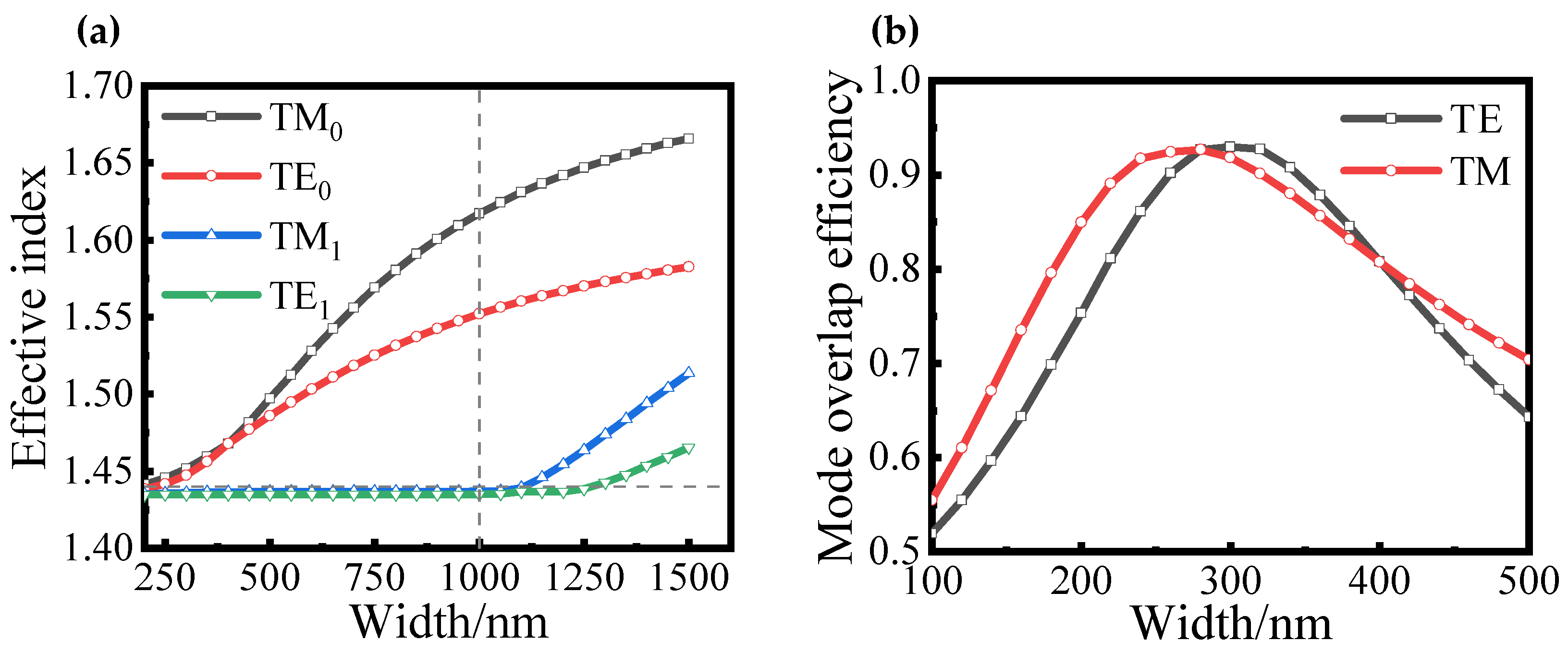
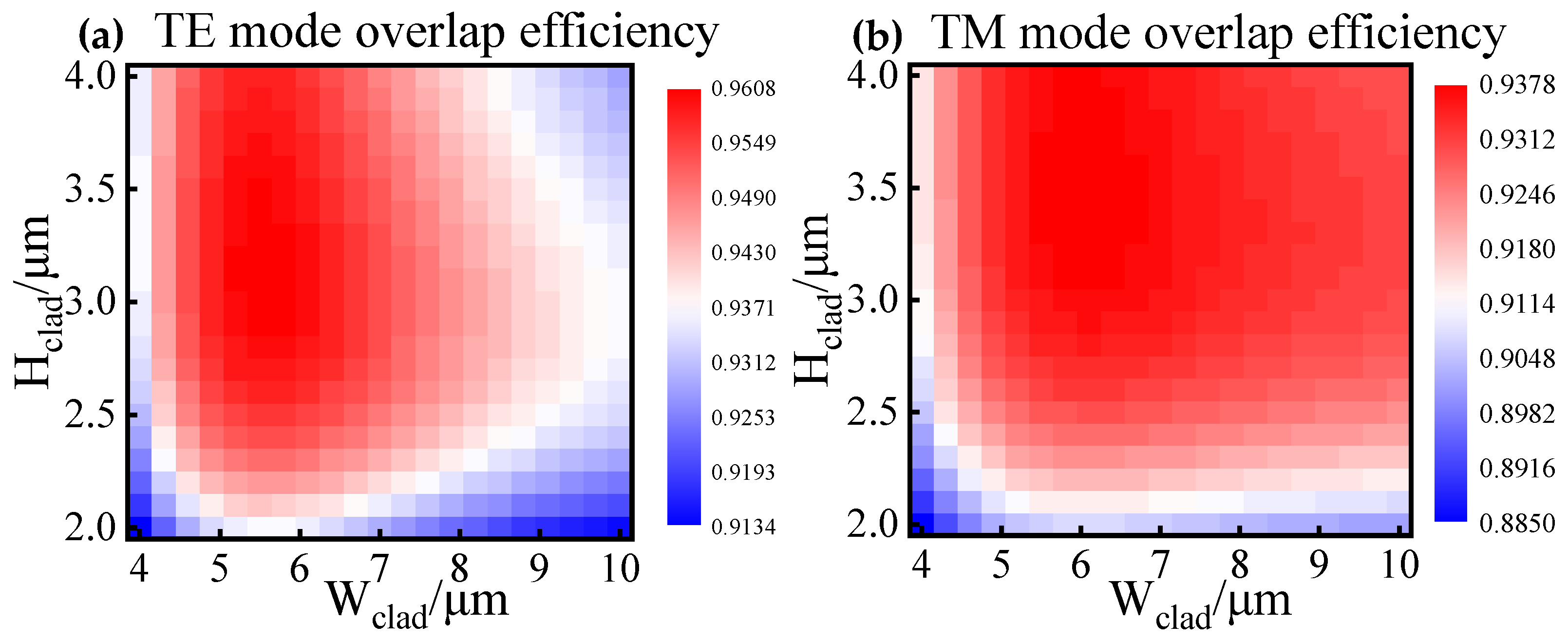
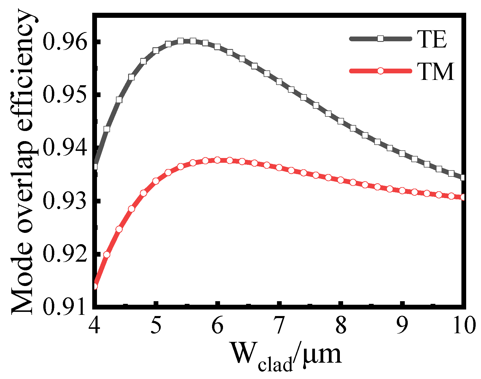
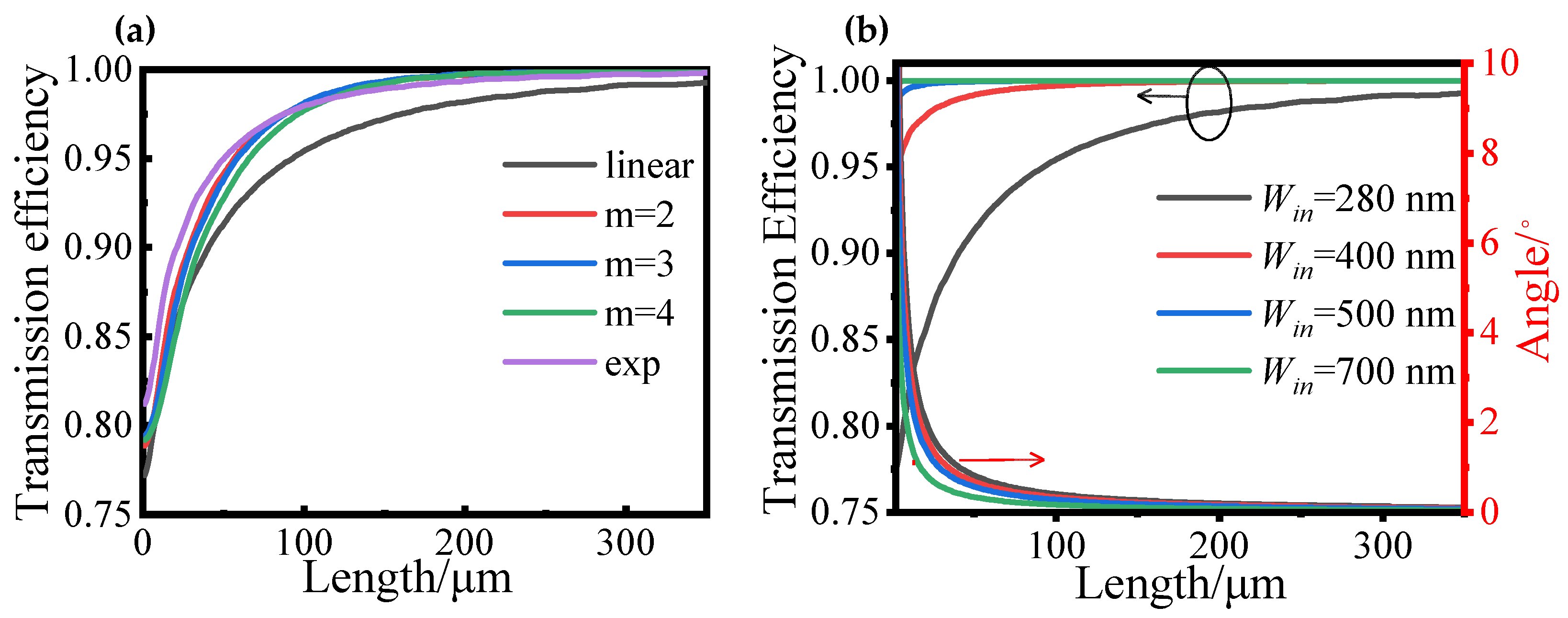
3.1. Mode Overlap Efficiency

According to the single-mode transmission conditions, the effective refractive index of the waveguide at various widths is studied using the Lumerical Finite Difference Eigenmode (FDE) Solver. Since the effective refractive index of the mode is less than the cladding refractive index, the mode cannot be transmitted in the waveguide in a stable state [24]. Figure 2a depicts the reference line of the effective refractive index of the cladding, and the output waveguide width Wout is determined to be 1000 nm when the waveguide contains solely TE0 and TM0 modes.
Figure 2b depicts the TE/TM mode overlap efficiency as a function of the waveguide input widths. When Hwaveguide is 400 nm, the mode overlap efficiency is calculated for the input waveguide end face and the high-NA fiber (MFD is 3.2 μm). For the TE mode, the maximum efficiency of 93.1% is reached when the waveguide width is 300 nm; for the TM mode, the maximum efficiency of 92.6% is reached when the waveguide width is 280 nm. Taking into account the manufacturing process and a reduction in the polarization sensitivity of the TE/TM mode, we determine the input waveguide width Win to be 280 nm, at which point the mode overlap efficiency of the TE/TM mode is almost the same, with improved polarization insensitivity.
As shown in Figure 1b, the innovative process is etched on both sides of the waveguide to create air slots to achieve better confinement, Wair is set to 2 μm, and Wclad and Hclad are optimized. Generally, we regard the parameters of the waveguide transverse confinement to be limitless. The analysis reveals that the width of the up cladding and BOX, as well as the thickness of the up cladding, have a significant impact on the coupling efficiency of the mode field and polarization insensitivity. Figure 3 shows the TE/TM mode overlap efficiency with different widths and heights. In Figure 3a, when Wclad is 5–6 μm and Hclad is greater than 2.5 μm, mode overlap efficiency does not change much with the increase in cladding thickness for the TE mode. The maximum mode overlap efficiency of TE is 96.1% when Wclad is 5.5 μm and Hclad is 3.2 μm. In Figure 3b, when Wclad is greater than 5 μm and Hclad is greater than 2.6 μm, the mode overlap efficiency of TM is relatively high, and when Wclad is 6.1 μm and Hclad is 3.7 μm, the TM mode overlap efficiency reaches the maximum of 93.8%. The TE/TM mode overlap efficiency has an adjustment space of 4.9%/5.2% when Wclad and Hclad are varied. Figure 4 illustrates the mode overlap efficiency of the TE/TM mode varies with width when Hclad is 3.6 μm. Eventually, Hclad/Wclad is decided to be 3.6 μm/6 μm to maximize polarization insensitivity. At this parameter, the mode overlap efficiency of TE increases by 2.8% to 95.9%, while that of TM increases by 1.2% to 93.8%, relative to the initial structure. These parameters are the result of evaluating the concurrent performance increase of the TE and TM modes. In addition, when without air slots, the simulated mode overlap efficiency of TE/TM at 1550 nm comes out to 92%/92.4%, which is 3.9%/1.4% lower than that with air slots. Therefore, the width of the cladding has a greater impact on the transverse mode field.
Because the width of the waveguide is 280 nm and the mode field restriction is weak in the transverse, it is necessary to decrease the transverse MFD by narrowing the thickness of the cladding so that the input waveguide optical field is as close as possible to the mode field of the Gaussian type. In the longitudinal direction, the waveguide height is 400 nm and is relatively strong for light confinement. To further improve the coupling efficiency of the TM mode field, it is necessary to provide a weaker cladding restriction in the longitudinal direction. HBOX is set at 4 μm and Hclad at 3.6 μm, resulting in a longitudinal restriction thickness of 7.6 μm, which is less than the transverse limitation of 6 μm. Through structural optimization, the mode field of the input waveguide is brought closer to the Gaussian beam, thereby improving the overall coupling efficiency and the device’s polarization insensitivity.
Altering the refractive index of the cladding can also affect the mode overlap efficiency. Although the BOX layer process of SOI wafers has been determined, the up cladding layer can slightly increase the refractive index by the doping process [25]. However, the change in refractive index during the manufacturing process can lead to a price increase. To simplify the model, this structure maintains the same refractive index for the up cladding and BOX layers.

3.2. Transmission Efficiency

It is clear that the coupling efficiency is determined by both mode overlap efficiency and transmission efficiency, and the design of the taper structure determines transmission efficiency. The general taper adopts linear, power-squared, and exponential structures, and the expression of the power-squared taper is [26]:
W ( x ) = W i n + ( x L t a p ) m × ( W o u t W i n ) ( 0 x L t a p )
where the value of m yields different power tapers, and Ltap is the length of the taper. The expression of the exponential taper structure is [13]:
W ( x ) = W i n + ( W o u t W i n ) { ( e x L t a p 1 ) / ( e 1 ) } ( 0 x L t a p )
Figure 5a illustrates transmission efficiency with the length for different tapers obtained by the Lumerical Eigenmode Expansion (EME) solver. The input waveguide (Win) is set to 280 nm, and the output waveguide (Wout) is set to 1000 nm, for all types of tapers. The linear taper has the lowest transmission efficiency at the same length. In contrast, the transmission efficiency of the power-squared and exponential taper is comparable, and both are greater than the linear taper because the angles of the power-squared and exponential taper fluctuate in real time. When the width of the waveguide is narrow, a smaller taper angle is more advantageous for mode transmission. Nonlinear tapers, however, are incapable of setting the angle according to the waveguide’s transmission efficiency, are more difficult to construct, and have a large fabrication tolerance, resulting in an inferior transmission. Especially for the exponential taper, and the power-squared taper for m = 4, transmission efficiency decreases slightly for the same reasons.
Figure 5b shows the TE mode transmission efficiency of the linear taper for different input waveguide widths and the relationship between the corresponding angles, where the taper angle can be calculated by:
θ = arctan [ ( W o u t W i n ) / L t a p ]
Ltap is the length of the taper, and Wout is fixed at 1000 nm; the width of the input waveguides (Win) are 280 nm, 400 nm, 500 nm, and 700 nm, respectively. The linear taper with the width of 280 nm has the lowest transmission efficiency at the same length, and the taper angle increases rapidly with a smaller taper length. In comparison with other input waveguide widths, to achieve the same transmission efficiency (98.9%), the Win of 280 nm requires a taper length of 276 μm, corresponding to a taper angle of 0.149 degrees; the Win of 400 nm requires a taper length of 40 μm and a taper angle of 0.859 degrees; the Win of 500 nm requires a taper length of 3 μm and a taper angle of 9.46 degrees. It can be determined that a narrower input waveguide width requires a longer taper length and a smaller taper angle to achieve high transmission efficiency. For a single taper structure, the waveguide’s width increases with the taper length; therefore, the structure must be implemented to achieve the variation of the taper angle with the length to achieve higher transmission efficiency and smaller device size.
As shown in Figure 1c, we designed the linear taper with four segments of different taper angles, and the transmission efficiency of each segment is increased as the width of the waveguide increases. The transmission efficiency for Taper1, Taper2, Taper3, and Taper4 are greater than 97.5%, 98.5%, 99.5%, and 99.9%, respectively. For a single linear taper with an input waveguide width of 280 nm and an output waveguide width of 1000 nm, the transmission efficiency of 97.5% can be achieved when the taper length is 156 μm and the taper angle is 0.26 degrees. At the same transmission efficiency, the taper length L1 required for a Taper1 structure with a waveguide width from 280 nm to 400 nm is 26 μm. When the input waveguide width is 400 nm, it is possible to obtain 98.8% transmission efficiency with a taper length of 36 μm, at which time the taper angle is 0.95 degrees and the taper length L2 of Taper2 is 6 μm. With an input waveguide width of 500 nm, 99.55% transmission efficiency may be reached with the taper length of 10 μm, the taper angle of 2.86 degrees; the taper length L3 of the Taper3 structure is 4 μm. When the input waveguide width is 700 nm, the taper length of 2 μm can achieve 99.9% transmission efficiency; the taper angle is 8.55 degrees and the length of L4 Taper4 is 2 μm. Finally, the total length of the four-segment linear taper structure obtained is only 38 μm. Table 2 is collated to obtain the optimized parameters of the four-segment linear taper.
Table 3 provides the transmission efficiency of the TE/TM mode for various structures when the length is 38 μm, as well as the length required for various structures to achieve TE transmission efficiency for the multi-segment taper. The multi-segment linear taper can significantly increase the transmission efficiency of TE polarization, and the same transmission efficiency can be achieved with only a quarter of the length of triadic taper. In addition, it can be shown that the transmission efficiency of the TM mode field does not vary much across different tapers, which is consistent with reality because the height of the taper structure remains constant at 400 nm. In addition, when without air slots, the simulated transmission efficiency of TE/TM at 1550 nm comes out 92%/92.4%, which is 0.64%/0.5% lower than that with air slots. This indicates that the air slots reduce the mode field leakage in the waveguide, where the waveguide is only weakly confined to the mode field, particularly at the stage of Taper1 and Taper2. It is apparent that the addition of air slots can increase the TE mode field transmission efficiency. The impact of air slots on transmission efficiency will be more pronounced for actual devices. Thus, multi-segment linear taper can improve the transmission efficiency of the TE mode in a compact size and have better polarization insensitivity.

3.3. Mode Field Distribution

The mode field distributions of the TE and TM in the XY direction of the multi-segment linear edge coupler are given in Figure 6a and Figure 7a. After passing through the edge coupler, the large-size mode field is gradually focused and finally is better constrained to the waveguide. Figure 6b–f and Figure 7b–f give the mode field for the TE and TM mode in the YZ cross section at locations of 0, 26, 32, 36, and 38 μm, respectively. In particular, the mode field of the TE/TM mode at X = 0 μm is approximately circular and has the same mode field radius in the Y/Z direction, which is similar to the Gaussian mode field. As the transmission distance increases, the mode field shrinks rapidly and is finally bound in the waveguide for transmission. It demonstrates this structure’s ability to realize the mode field transition with a compact footprint.

3.4. Wavelength Dependence

Figure 8 depicts the coupling loss for various polarization ranging from 1000 nm to 2150 nm with and without air slots. When the air slots are present, the coupling loss for the TE and TM modes at λ = 1550 nm is 0.22 dB and 0.31 dB, respectively, with the TE mode having the lowest coupling loss at this wavelength. The minimum coupling loss at λ = 1650 nm is 0.216 dB for the TM mode. Without air slots, the coupling loss at λ = 1550 nm is 0.42 dB and 0.37 dB for TE and TM modes, respectively. As the mode overlap efficiency decreases and the leakage of the mode field increases, the coupling loss of TE/TM increases rapidly compared with air slots for the long-wave direction. Therefore, air slots can effectively minimize coupling loss. With and without air slots, the coupling loss increases rapidly in the short-wave direction, resulting from stronger restriction of the mode field and lower mode overlap efficiency for couplers in the short wavelength. Lastly, the coupling loss of TE/TM polarization is less than 1 dB in the range of 1400~1850 nm, indicating that the designed structure is wavelength insensitive and can work efficiently in the wide wavelength bandwidth (S-, C-, L-, and U-band).

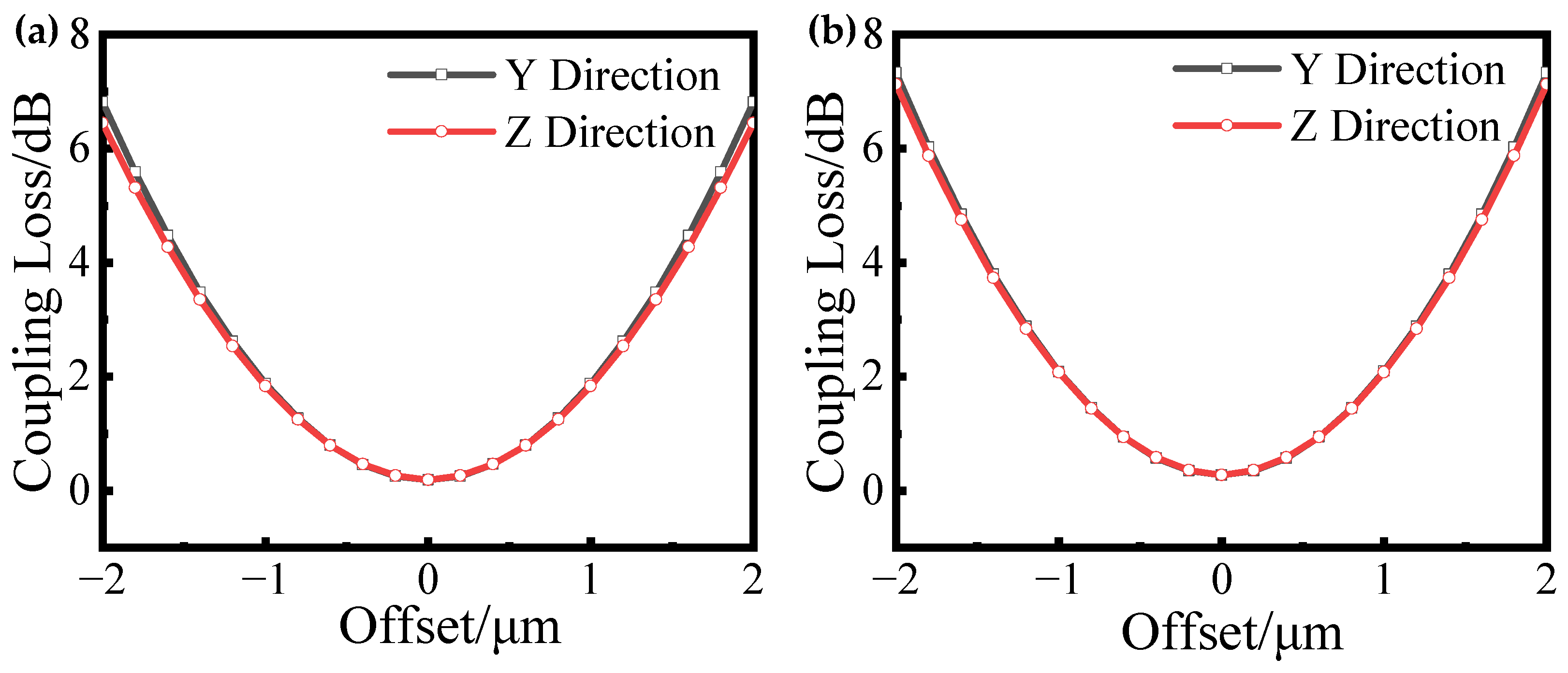
3.5. Alignment Tolerance

Alignment tolerance is an important measure of the performance of an optical coupling system. A good alignment tolerance facilitates the construction of subsequent device packages. The alignment tolerance of the device is analyzed by shifting the fiber position in the Y/Z direction to obtain the coupling loss, and the curve is obtained as shown in Figure 9. For the TE mode, the 3-dB alignment tolerance of the fiber and coupler is ±1.4 μm/±1.4 μm in the Y/Z direction and is ±1.3 μm/±1.35 μm in the Y/Z direction for the TM mode. Therefore, the multi-segment taper coupler has a better alignment tolerance, which makes the post-encapsulation simpler and more reliable.

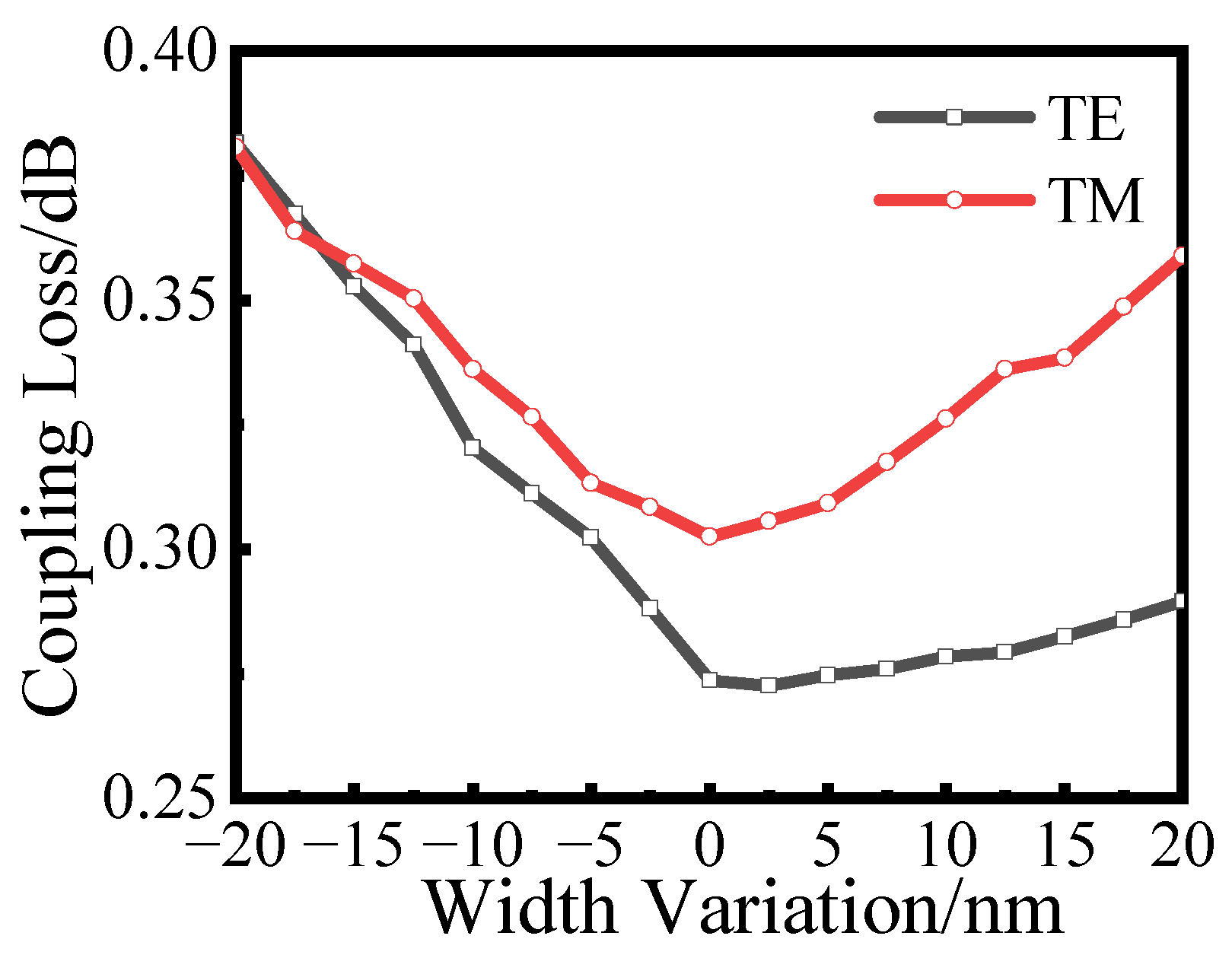
3.6. Fabrication Variation

In addition, during the lithography process, the performance of the manufacturing equipment has an impact on the device performance, introducing fabrication tolerances. The effect of the evaluated width variation (ΔW) is ±20 nm on the coupling loss. Figure 10 demonstrates that the effect of width variation for the TE/TM mode is less than 0.2 dB and the TM mode is less vulnerable to fabrication variation. It demonstrates that this structure has a good fabrication tolerance and can be effectively fabricated using standard CMOS processes.

4. Discussion

The preparation process of the proposed structure is comparatively straightforward and versatile and can be implemented using standard CMOS processes with a minimum process size of 280 nm. In addition, the change in thickness of the up cladding from 3 μm to 8 μm has been experimentally validated [13,25,27]; the thickness of the up cladding is 3.6 μm, with minimal impact on the performance of other devices. Due to the introduction of air slots, the edge coupler must be hermetically packaged to prevent contamination. However, the majority of photonic integrated circuits are already hermetically packaged, so the increase in total cost of packaging is minimal. Finally, we make a comprehensive comparison between previously reported fiber-to-chip edge couplers and the proposed structure from total length, coupling loss, bandwidth, and MFD, as listed in Table 4. It is demonstrated that the proposed structure can be made very short along its total length, has a large advantage in terms of coupling loss, and has a broad bandwidth compared to previously reported devices. The structure can be realized on a standard CMOS process and can be applied to large-scale fiber-to-chip coupling in optical interconnectivity.

5. Conclusions

We present a high-efficiency and compact polarization-insensitive multi-segment linear silicon nitride edge coupler, which can achieve efficient chip-to-fiber coupling with a total length of 38 μm. In particular, the design improves the polarization insensitivity of the TE/TM mode by optimizing the thickness of the up cladding and introducing air slots in the lateral direction to change the lateral optical field confinement. The mode overlap efficiency can be reached at 95.9%/93.8%, and the coupling loss is 0.22 dB/0.31 dB for the TE/TM mode at λ = 1550 nm. The coupling loss of the TE and TM modes is less than 1 dB in the range of 1400~1850 nm, which indicates that the device is wavelength insensitive; the 3-dB alignment tolerance between fiber and coupler is ±1.4 μm/±1.4 μm in the Y/Z direction for the TE mode and is ±1.3 μm/±1.35 μm in the Y/Z direction for the TM mode. The variation in coupling loss is less than 0.2 dB at a fabrication variation of ±20 nm, and the effect of fabrication variation is small. Thus, this work provides a new idea for realizing highly efficient and compact polarization-insensitive silicon nitride edge couplers, providing fundamental support for the realization of compact photonic devices with high-density integration in silicon photonic integrated circuits.

Author Contributions

Conceptualization, Y.Z., Y.L., X.C. and L.W.; methodology, Y.Z. and Y.L.; software, Y.Z. and W.C.; validation, Y.Z., Y.L., X.C. and C.M.; formal analysis, Y.Z., Y.L., X.C. and L.W.; investigation, Y.Z. and Y.L.; resources, M.L., N.Z. and W.C.; data curation, Y.Z. and W.C.; writing—original draft preparation, Y.Z.; writing—review and editing, Y.Z. and W.C.; visualization, Y.Z.; supervision, W.C.; project administration, W.C.; funding acquisition, W.C. All authors have read and agreed to the published version of the manuscript.

Funding

This research was supported in part by the National Key Research and Development Program of China under Grant 2020YFB2205901.

Institutional Review Board Statement

Not applicable.

Informed Consent Statement

Not applicable.

Data Availability Statement

Not applicable.

Conflicts of Interest

The authors declare no conflict of interest.

References

  1. Siew, S.Y.; Li, B.; Gao, F.; Zheng, H.Y.; Zhang, W.; Guo, P.; Xie, S.W.; Song, A.; Dong, B.; Luo, L.W.; et al. Review of Silicon Photonics Technology and Platform Development. J. Light. Technol. 2021, 39, 4374–4389. [Google Scholar] [CrossRef]
  2. Margalit, N.; Xiang, C.; Bowers, S.M.; Bjorlin, A.; Blum, R.; Bowers, J.E. Perspective on the Future of Silicon Photonics and Electronics. Appl. Phys. Lett. 2021, 118, 220501. [Google Scholar] [CrossRef]
  3. Rickman, A. The Commercialization of Silicon Photonics. Nat. Photonics 2014, 8, 579–582. [Google Scholar] [CrossRef]
  4. Tang, M.; Park, J.-S.; Wang, Z.; Chen, S.; Jurczak, P.; Seeds, A.; Liu, H. Integration of III-V Lasers on Si for Si Photonics. Prog. Quantum Electron. 2019, 66, 1–18. [Google Scholar] [CrossRef]
  5. Dong, P.; Qian, W.; Liao, S.; Liang, H.; Kung, C.-C.; Feng, N.-N.; Shafiiha, R.; Fong, J.; Feng, D.; Krishnamoorthy, A.V.; et al. Low Loss Shallow-Ridge Silicon Waveguides. Opt. Express 2010, 18, 14474–14479. [Google Scholar] [CrossRef]
  6. Blumenthal, D.J.; Heideman, R.; Geuzebroek, D.; Leinse, A.; Roeloffzen, C. Silicon Nitride in Silicon Photonics. Proc. IEEE 2018, 106, 2209–2231. [Google Scholar] [CrossRef]
  7. Marchetti, R.; Lacava, C.; Carroll, L.; Gradkowski, K.; Minzioni, P. Coupling Strategies for Silicon Photonics Integrated Chips [Invited]. Photon. Res. 2019, 7, 201. [Google Scholar] [CrossRef]
  8. Moss, D.; Miao, Y.; Ta’eed, V.; Mägi, E.; Eggleton, B. Coupling to High-Index Waveguides via Tapered Microstructured Optical Fibre. Electron. Lett. 2005, 41, 1. [Google Scholar] [CrossRef]
  9. Mu, X.; Wu, S.; Cheng, L.; Fu, H.Y. Edge Couplers in Silicon Photonic Integrated Circuits: A Review. Appl. Sci. 2020, 10, 1538. [Google Scholar] [CrossRef]
  10. Hatori, N.; Shimizu, T.; Okano, M.; Ishizaka, M.; Yamamoto, T.; Urino, Y.; Mori, M.; Nakamura, T.; Arakawa, Y. A Hybrid Integrated Light Source on a Silicon Platform Using a Trident Spot-Size Converter. J. Light. Technol. 2014, 32, 1329–1336. [Google Scholar] [CrossRef]
  11. Hettrick, S.J.; Wang, J.; Li, C.; Wilkinson, J.S.; Shepherd, D.P. An Experimental Comparison of Linear and Parabolic Tapered Waveguide Lasers and a Demonstration of Broad-Stripe Diode Pumping. J. Light. Technol. 2004, 22, 845–849. [Google Scholar] [CrossRef]
  12. Ren, G.; Chen, S.; Cheng, Y.; Zhai, Y. Study on Inverse Taper Based Mode Transformer for Low Loss Coupling between Silicon Wire Waveguide and Lensed Fiber. Opt. Commun. 2011, 284, 4782–4788. [Google Scholar] [CrossRef]
  13. Bhandari, B.; Im, C.-S.; Lee, K.-P.; Kim, S.-M.; Oh, M.-C.; Lee, S.-S. Compact and Broadband Edge Coupler Based on Multi-Stage Silicon Nitride Tapers. IEEE Photonics J. 2020, 12, 1–11. [Google Scholar] [CrossRef]
  14. Teng, M.; Niu, B.; Han, K.; Kim, S.; Xuan, Y.; Lee, Y.J.; Qi, M. Trident Shape SOI Metamaterial Fiber-to-Chip Edge Coupler. In Proceedings of the Optical Fiber Communication Conference (OFC), San Diego, CA, USA, 3–7 March 2019; OSA: San Diego, CA, USA, 2019; p. Tu2J.6. [Google Scholar]
  15. Mu, X.; Wu, S.; Cheng, L.; Tu, X.; Fu, H.Y. Ultra-Compact Silicon Photonic Edge Coupler Based on Subwavelength Gratings. In Proceedings of the Asia Communications and Photonics Conference, Chengdu, China, 2–5 November 2019. [Google Scholar]
  16. Li, Y.; Wang, M.; Yang, S.; Quan, X.; Xu, J.; Wu, L.; Liu, M.; Cheng, X. Polarization Insensitive Edge Coupler Assisted by Subwavelength Grating and Suspended Structure. IEEE Photon. Technol. Lett. 2022, 34, 765–768. [Google Scholar] [CrossRef]
  17. Wang, X.; Quan, X.; Liu, M.; Cheng, X. Silicon-Nitride-Assisted Edge Coupler Interfacing With High Numerical Aperture Fiber. IEEE Photon. Technol. Lett. 2019, 31, 349–352. [Google Scholar] [CrossRef]
  18. Yao, Z.; Wan, Y.; Zhang, Y.; Ma, X.; Zheng, Z. Broadband High-Efficiency Triple-Tip Spot Size Converter for Edge Coupling with Improved Polarization Insensitivity. Opt. Commun. 2020, 475, 126301. [Google Scholar] [CrossRef]
  19. Sun, S.; Chen, Y.; Sun, Y.; Liu, F.; Cao, L. Novel Low-Loss Fiber-Chip Edge Coupler for Coupling Standard Single Mode Fibers to Silicon Photonic Wire Waveguides. Photonics 2021, 8, 79. [Google Scholar] [CrossRef]
  20. Wu, D.; Yan, W.; Yang, Y.; Song, X.; Wei, Z.; Qin, J.; Deng, L.; Bi, L. A Theoretical Sub-0.1 DB Loss Single Mode Fiber-To-Chip Edge Coupler for Silicon Nitride Waveguides. Photonics 2023, 10, 231. [Google Scholar] [CrossRef]
  21. Snyder, A.W.; Love, J.D. Optical Waveguide Theory; Chapman and Hall: London, UK, 1983; Volume 175. [Google Scholar]
  22. Liu, Y.; Chen, W.; Zhang, Y.; Cao, K.; Liu, Y.; Li, M.; Zhu, N. High-Efficiency Spot-Size Converter for Thin-Film Lithium Niobate Modulators. In Proceedings of the AOPC 2022: Optoelectronics and Nanophotonics, Beijing, China, 26–28 June 2022; Cheng, B., Guo, J., Qian, S., Eds.; SPIE: Beijing, China, 2023; p. 29. [Google Scholar]
  23. Yin, P.; Serafini, J.R.; Su, Z.; Shiue, R.-J.; Timurdogan, E.; Fanto, M.L.; Preble, S. Low Connector-to-Connector Loss through Silicon Photonic Chips Using Ultra-Low Loss Splicing of SMF-28 to High Numerical Aperture Fibers. Opt. Express 2019, 27, 24188. [Google Scholar] [CrossRef]
  24. Chuang, S.L. Physics of Photonic Devices; John Wiley & Sons: Hoboken, NJ, USA, 2012. [Google Scholar]
  25. Liang, Y.; Li, Z.; Fan, S.; Feng, J.; Liu, D.; Liao, H.; Yang, Z.; Feng, J.; Cui, N. Ultra-Low Loss SiN Edge Coupler Interfacing with a Single-Mode Fiber. Opt. Lett. 2022, 47, 4786. [Google Scholar] [CrossRef]
  26. Li, D.; Li, B.; Tang, B.; Zhang, P.; Yang, Y.; Liu, R.; Xie, L.; Li, Z. High Efficiency and Compact Vertical Interlayer Coupler for Silicon Nitride-on-Silicon Photonic Platform. Optik 2023, 274, 170572. [Google Scholar] [CrossRef]
  27. Tang, L.; Li, L.; Li, J.; Chen, M. Hybrid Integrated Ultralow-Linewidth and Fast-Chirped Laser for FMCW LiDAR. Opt. Express 2022, 30, 30420. [Google Scholar] [CrossRef] [PubMed]
  28. Yang, Y.; Gao, K.; Zhang, H.; Liu, H.; Lu, X.; Ren, X.; Huang, Y. Design of Silicon Nitride Edge Coupler for Monolithically Integrated Laser on Silicon Photonic Circuits With Relaxed Alignment Tolerance and High Efficiency. IEEE Photonics J. 2022, 14, 1–6. [Google Scholar] [CrossRef]
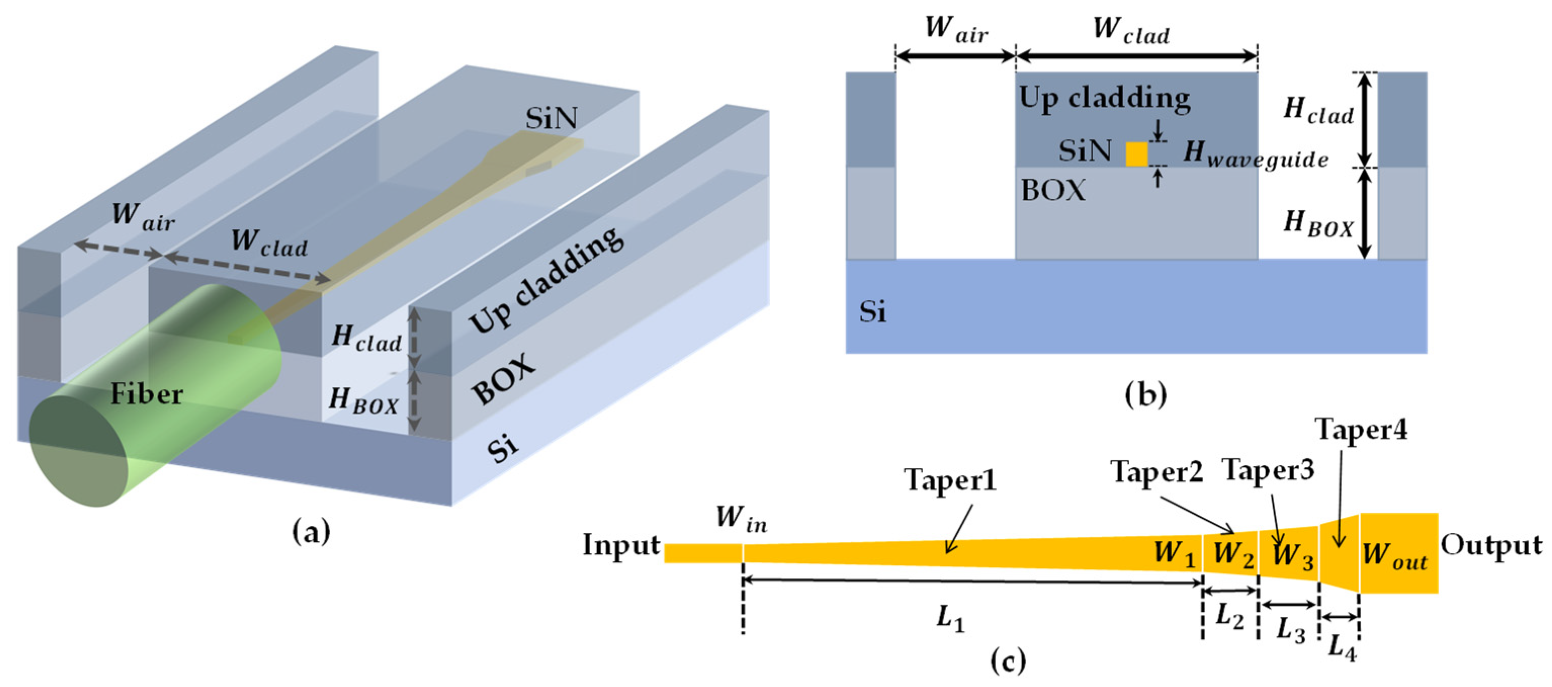
Figure 1. (a) Schematic structure of multi-segment linear edge coupler. (b) Side view of multi-segment linear edge coupler. (c) Top view of silicon nitride waveguide.
Photonics 10 00510 g001
Figure 2. (a) The curve of effective refractive index with different waveguide widths. (b) The curve of mode overlap efficiency with different input waveguide widths.
Photonics 10 00510 g002
Figure 3. The mode overlap efficiency with different clad widths and heights. (a) TE. (b) TM.
Photonics 10 00510 g003
Figure 4. When Hclad is 3.6 μm, the curve of mode overlap efficiency with different cladding widths.
Photonics 10 00510 g004
Figure 5. (a) The curves of transmission efficiency with the length of different tapered structures. (b) TE transmission efficiency and its corresponding angle curve with the length for different input waveguide widths.
Photonics 10 00510 g005
Figure 6. TE mode field distribution. (a) XY direction mode field. (bf) YZ direction mode field at X = 0, 26, 32, 36, 38 μm.
Photonics 10 00510 g006
Figure 7. TM mode field distribution. (a) XY direction mode field. (bf) YZ direction mode field at X = 0, 26, 32, 36, 38 μm.
Photonics 10 00510 g007
Figure 8. Coupling loss of structures with and without air slots in the function of wavelength.
Photonics 10 00510 g008
Figure 9. Fiber-to-chip alignment tolerances for different modes. (a) TE. (b) TM.
Photonics 10 00510 g009
Figure 10. Coupling loss at different fabrication tolerance.
Photonics 10 00510 g010
Table 1. Optimized parameters of the designed edge coupler.
DimensionSize/μmDimensionSize/μm
HBOX4W20.5
Hclad3.6W30.7
Hwaveguide0.4Wout1
Wclad6L126
Wair2L26
Win0.28L34
W10.4L42
Table 2. Structural parameters and efficiency of single tapers and the proposed multi-segment taper parameters.
Width of Input to Output for Single Linear Taper LengthTaper AngleTransmission Efficiency Width of Input to OutputTaper Length
280 nm to 1000 nm156 μm0.26°97.5%Taper1280 nm to 400 nm26 μm
400 nm to 1000 nm36 μm0.95°98.8%Taper2400 nm to 500 nm6 μm
500 nm to 1000 nm10 μm2.86°99.55%Taper3500 nm to 700 nm4 μm
700 nm to 1000 nm2 μm8.55°99.9%Taper4700 nm to 1000 nm2 μm
Table 3. Comparison of transmission efficiency of different structures.
StructuresTETMLength of TE Transmission Efficiency for Multi-Segment Taper
Linear taper89.3%98.1%338 μm
Parabolic taper (m = 2)91.9%98.9%142 μm
Triadic taper (m = 3)91.4%99.1%137 μm
Quadratic taper (m = 4)90.4%99.1%148 μm
Exponential taper92.4%99.3%173 μm
This structure99.34%99.9%38 μm
Table 4. Device comparisons between typical fiber-to-chip edge couplers.
Device StrictureLength/μmCoupling Loss/dBBandwidth/nmMFD/μm
Multi-Stage taper [13]760.36/0.55 *965 (<3 dB)4 [E]
Subwavelength grating [16]5500.86/0.94 *-10.4 [S]
Multi-layer structure [17]3000.35/0.9 *95 (<1 dB)6.5 [E]
triple-tip taper [18]600.5/0.5 *580 (<1 dB)3 [S]
multiple structure [19]4500.7(TE)-8.2 [S]
inverted taper [25]-0.85/1.09 *130 (<1 dB)10 [E]
bi-layer 5-tip [28]38.20.33(TE)362 (<1 dB)N.A. [S]
This work380.22 /0.31 * 450 (<1 dB)3.2 [S]
XX/XX *: represents coupling loss of TE/TM mode, respectively. E: experiment results, S: simulation results; “-”: not mentioned.
Disclaimer/Publisher’s Note: The statements, opinions and data contained in all publications are solely those of the individual author(s) and contributor(s) and not of MDPI and/or the editor(s). MDPI and/or the editor(s) disclaim responsibility for any injury to people or property resulting from any ideas, methods, instructions or products referred to in the content.

