Abstract
Bismuth shows outstanding optical properties, including a metal-like response in the ultraviolet-visible range and a dielectric character with a giant refractive index in the infrared range. In recent years, such unique properties have been employed to construct bismuth-based metamaterials with remarkable optical responses in these spectral regions, especially with cost-effective lithography-free methods. Such responses can be manipulated, both in an astatic way by suitable metamaterial design and in a dynamic way by harnessing the solid–liquid transition of bismuth. In this paper, we review the advances in this field and highlight the applications of such metamaterials to information technology production, energy harvesting and sensing.
1. Introduction
In recent years, optical metamaterials have been intensively studied for their potential on highly efficient sub-wavelength devices, as well as their values in applications such as perfect absorbers, high selective color filters, optical switching, photodetection, light guiding, optical cloaking, etc. [1,2,3,4]. Usually, optical metamaterials have a highly specific designed geometric structure with rigorous requirements for their material properties. As such, effective and robust fabrication of the desired structures as well as the rational design or selection of the suitable materials are both critical to achieve superior optical metamaterials.
On the topic of fabrications, several innovative routes have been developed to meet the requirement to prepare the optical metamaterials [5,6,7]: ultraviolet (UV) or electron beam lithography (EBL) [8,9], focused ion beam (FIB) milling [10], deposition-induced structuring [11], dewetting-induced nanoscale self-formation [12], oblique angle deposition of three-dimensional structures [13], template-assisted etching and deposition [14], and laser direct writing, are examples of these methods [15]. Among them, several advanced nanoscale fabrication techniques such as UV or EBL, and FIB, are either costly or present a low throughput, so that alternative “lithography-free” fabrication approaches are desired to provide, at a larger scale, nanomaterials with a tailored optical response suitable for applications [16].
On the topic of material design and selection, semiconductors and noble metals (Ag, Au, etc.) are the initial choices to conceptualize optical metamaterials from abnormal transmission to various plasmonic resonances, photonic crystals or cavities [17,18,19,20]. Afterward, lossy metals, doped metal oxides, and metal nitrides are utilized in a proper configuration for extended working wavelength regimes to short-wavelength infrared (SWIR) or even mid-wavelength infrared (MWIR) regimes with plasmonic responses [21,22,23,24,25]. Moreover, in longer wavelengths, 2D materials, metal oxides, highly doped semiconductors and polar materials are suitable candidates [26,27]. Besides these materials, Bi shows unique properties that are worth investigating. Several metamaterials based on bulky or nano-dimension bismuth have been reported in recent years and exhibit various singular classical and quantum phenomena from abnormal surface-state effects to high-order topology [28,29,30]. The unique band structure of bismuth [31] allows interband plasmons in the UV–Vis regime, Mie resonance in the SWIR and regime, and “free-carrier” plasmons in the far-infra (FIR) and THz regimes simultaneously (Figure 1) [32]. As such, Bi is valuable to construct metamaterials over extremely broad wavelength ranges.

Figure 1.
Multiple resonances feasible on bismuth from UV to FIR and even THz regime (MWIR: mid-wavelength infrared; LWIR: long-wavelength infrared; FIR: far-infrared).
In this review paper, lithography-free Bi metamaterials, as a promising system combining preferable fabrication methods and excellent optical function, is our focus. We track the recent advances of Bi meta material for light manipulation, from absorbing to filtering and switching, highlight the most recent scientific discoveries and forecast the future trends of this field as well as its applications. The rest of this paper is organized as follows: Section 2 discusses the basic electronic and optical properties of Bi; Section 3 describes the various lithography-free fabrication methods of Bi metamaterials; and Section 4 focuses on the emerging function devices based on Bi metamaterials for light manipulation. Lastly, conclusions and perspective are drawn in Section 5.
2. Fundamental Optoelectronic Properties of Bi
2.1. Electronic Band Structure
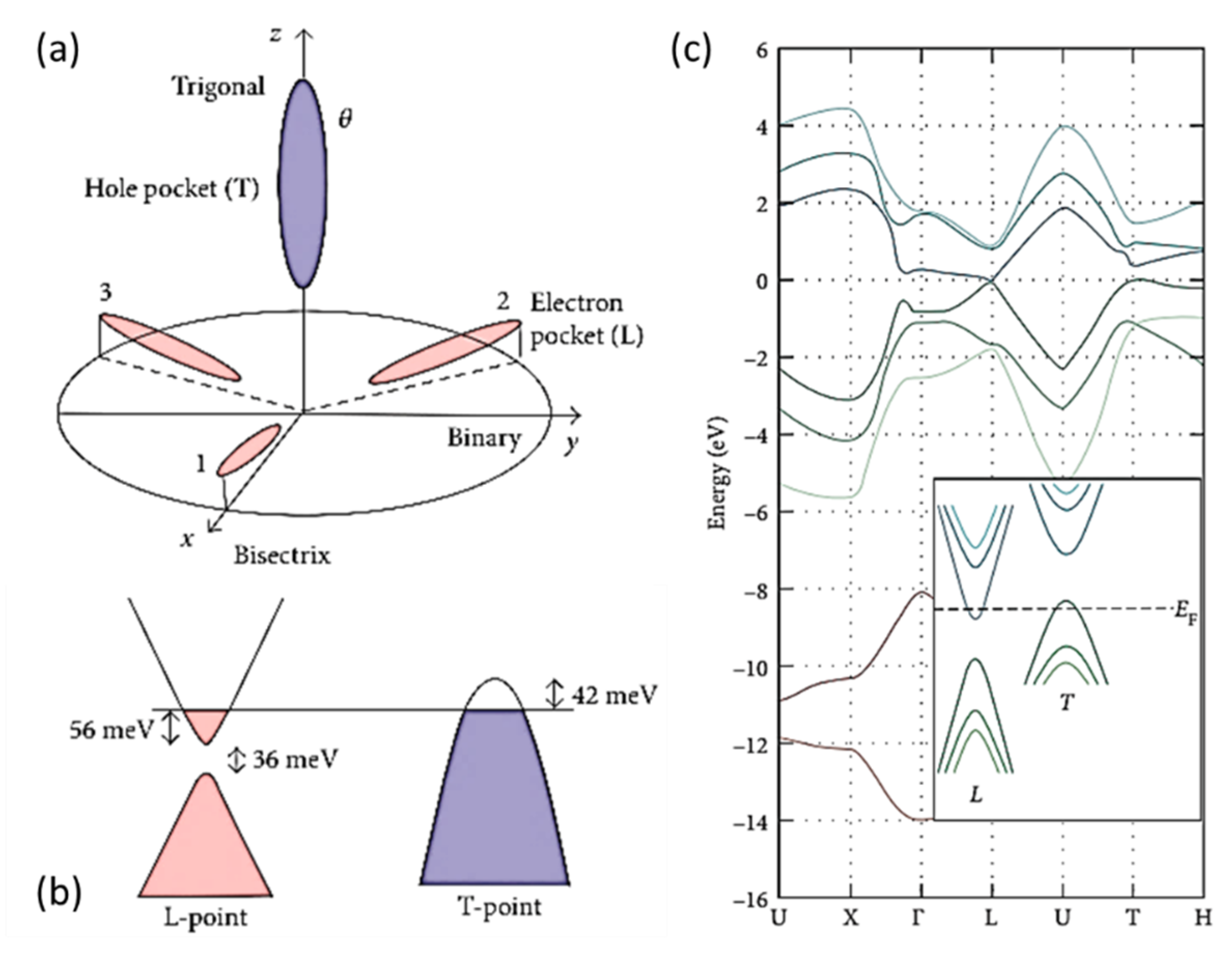
As a p-block semimetal, bismuth has a distinct electronic band structure with several exceptional physical characteristics, such as a long charge carrier mean-free path (~1 μm at room temperature) [33], anisotropic thermal electronic behavior [34], enormous magnetoresistance [35], and/or quantum confinement phenomena [36,37]. It displays a highly anisotropic Brillouin zone (Figure 2a) with threefold symmetrical electron pockets near the three equivalent L-points and one hole pocket near the T-point [32,37]. At room temperature (RT), the electron and hole Fermi energy levels are, respectively, 56 meV at the and 36 meV at the L-point. The direct band gap at the T-point has an energy of 42 meV (Figure 2b) [32,38]. These band structure features make Bi semi-metallic. Accordingly, Presents a very low free-carrier density NBi ranging from 1018 to 1019 cm−3. Moreover, Bi is endowed with a wide diversity of lower-lying energy bands, as demonstrated in the band diagram of bismuth (Figure 2c) [32,39], which is critical to the optical response in the UV, Vis, and IR ranges, as will be seen below, whereas free charge carriers involving Bi’s semi-metallic conduction can primarily influence its far-IR and THz light responses.
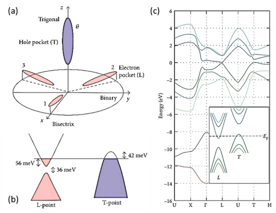
Figure 2.
(a) Brillouin zone of bismuth in the momentum space; (b) electronic band structure of Bi near the Fermi level at room temperature; (c) calculated full band diagram of Bi accounting for the spin-orbit coupling (reprinted with permission from [32] © 2018 under CC BY 4.0 license).
2.2. Optical Dielectric Function of Bismuth
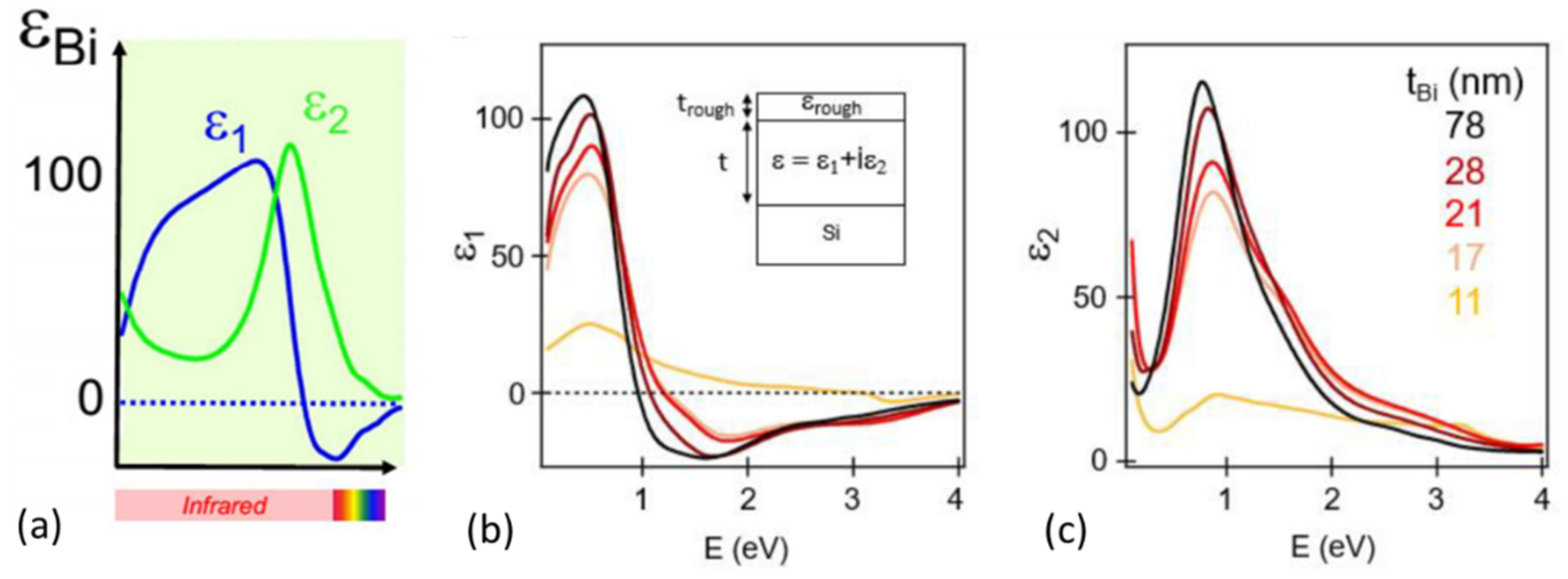
Despite the fact that Bi is an intriguing element with a complex electronic band structure that affects its optical response, as stated in Section 2.1, its optical properties have hardly been explored. Early investigations into the optical dielectric function ε = ε1 + iε2 of bulk Bi were carried out in a narrow spectral range, and in these results, Bi had a relatively broad dispersion that may have been caused by poor sample quality [40]. Until recent years, optical characterizations of both Bi crystals and films were refined thanks to the efforts of Johann To udert et al. on spectroscopic ellipsometry, thoroughly from the far-IR to the UV on high-quality Bi thin films [41]. According to their work, the Kramers–Kronig consistent dielectric function of the Bi material (Figure 3a) was constructed. It was found that ε1 < 0 in the UV, Vis, and near-IR regions, thus supporting the plasmonic responses in this region due to the giant interband transitions in SWIR around 0.8 eV. This strong absorption band was associated with interband transitions with an onset near the Γ point according to the report of Hunderi [42], as well as later theoretical calculations of the band structure by Liu and Allen [38]. On the other hand, ε1 in the far-IR and THz ranges is also negative but this could be ascribed to the contribution of the free carrier. Therefore, other than the conventional plasmonic resonances of noble metals in the UV–V is range produced by the collective excitation of the free electrons, Biexhibits so-called “interband plasmonic” resonances in these regimes [40,43], while its collective excitation of free carriers exist in the far-IR and THz regions owing to its quite small NBi. This is in line with the fact that the p-bands of Bi cross the Fermi level at the T and L points of the Brillouin zone, creating hole pockets at the T points and electron pockets at the L points. These pockets are very shallow (tenths of meV), and this in turn leads to a very low carrier density [41]. Between the interband and free-carrier plasmonic regions, high positivity (ε1~100) of Bi could induce strong dielectric Mie resonances in the SWIR and MWIR regimes [40,43]. Johann Toudert et al. further explored the size effect of the bismuth dielectric response, specifically checking the evolution of the dielectric function of bismuth thin films with different thickness [44]. As shown in Figure 3b, for ε1 and ε2 spectrum, respectively, at the photon energies from the FIR to the UV range, the Bi films with a nominal thickness equal to or larger than 17 nm present a dielectric function similar to the bulk one. However, the film with a 11 nm nominal thickness presented a dielectric function very different from the bulk film due to the effective medium behavior of the discontinuous film. Such a thickness dependence of the bismuth dielectric response provides quite valuable clues for the development of Bi metamaterials, which often involves the nanostructure level [45].
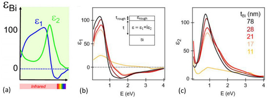
Figure 3.
(a) Optical dielectric function of bulky bismuth from UV to FIR (reprinted with permission from [41] ©2017 American Chemical Society); (b) ε1 and (c) ε2 spectrum of Bi thin film with different thickness (reprinted with permission from [44] © 2019 Optics Society of America under CC BY 4.0 license).
3. Lithography-Free Fabrication of Bismuth Metamaterials
It is well known that the optical metamaterials are usually constructed by specific designed nanostructures, whose preparations are highly dependent on the lithography and related nano-fabrication tools [1,2,6,46]. However, these lithography-based fabrication methods are often complicated and not cost-effective. Hence, in the investigation of bismuth metamaterial, developing lithography-free fabrication methods are highly desired. So far, the bismuth thin film, the bismuth nanoparticles embedded in a dielectric matrix, and the bismuth nanorod array are applied as the optical metamaterials for absorbers [45,47,48,49,50,51,52], filters [49,53,54], and analog tuners for intensity and phase [55,56,57], as well as for thermal-optical switching [54,58,59]. Additionally, they can be prepared via lithography-free routes including regular physical vapor deposition (PVD) via magnetron sputter or thermal evaporation [32],pulse laser deposition (PLD) [60], and glazing-angle deposition (GLAD) [57]. Moreover, by combining this with some templates such as anodized aluminum oxide (AAO), which is quite practical for nano-bismuth fabrications [32], several more ordered bismuth structures might be also lithography-free prepared. In the following paragraphs, they will be discussed one after another.
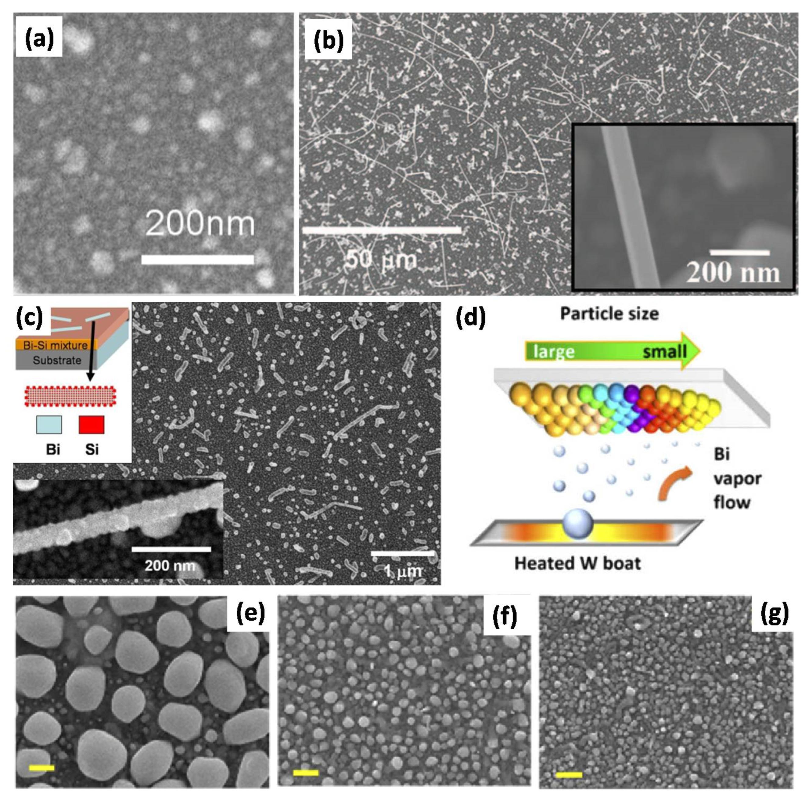
PVD is widely used to prepare the thin film, and accordingly is feasible as a metamaterial absorber or reflective color filter based on bismuth thin film [21,32,61]. Magnetron sputter is one of most frequently used PVD methods, involving a gaseous plasma which is generated and confined to a space around the target. The plasma liberates atoms traveling through the vacuum chamber and deposit them onto a substrate to form a thin film. Thermal evaporation using resistors or electron-beam heating is another kind of film-deposition route [62]. In recent years, the PVD deposition of bismuth have been intensively studied (Figure 4a–g) [21,32,61,63]; aside from regular thin film, some other non-trivial products such as nanowires or nanorods can also be obtained due to the unique physical and chemical properties of Bi, which include anisotropic surface transportation [61], self-catalyzation [64], the stress-effect [33] and surfaced wetting [21]. By artfully combining thermodynamic and kinetic features of the thermally-evaporated bismuth, various sizes of core–shell bismuth nanoparticles are fabricated on a large-area silicon substrate using a one-step thermal evaporation deposition process, which show spectral shifts and full visible colors in a hue order with a color gamut that is close to sRGB [62]. Considering the values of the Bi nanostructures for metamaterial applications [47,57], there is no doubt that these results could provide more clues for the PVD-based lithography-free fabrication of Bi metamaterials.
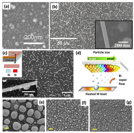
Figure 4.
Nanoscale Bi products obtained by PVD techniques including (a) Bi thin film fabricated by magnetron sputter at room temperature(reprinted with permission from [21] © 2017 Optics Society of America under CC BY 4.0 license); (b) Bi nanowire prepared by magnetron sputter under a low deposition rate, its inset showing the diameter of the wire at ~80 nm (reprinted with permission from [61] © 2012 AIP Publishing under CC BY 3.0 license); and (c) Bi nanorod/Si nanodot hybrid structure grown by a surface-dewetting effect during magnetron sputter deposition(reprinted with permission from [21] © 2017 Optics Society of America under CC BY 4.0 license). (d) One-step thermal evaporation deposition of the Bi nanoparticle with various average diameters from (e) 614 nm, to (f) 151 nm, and to (g) 84 nm (reprinted with permission from [62] © 2020 Optics Society of America under CC BY 4.0 license).
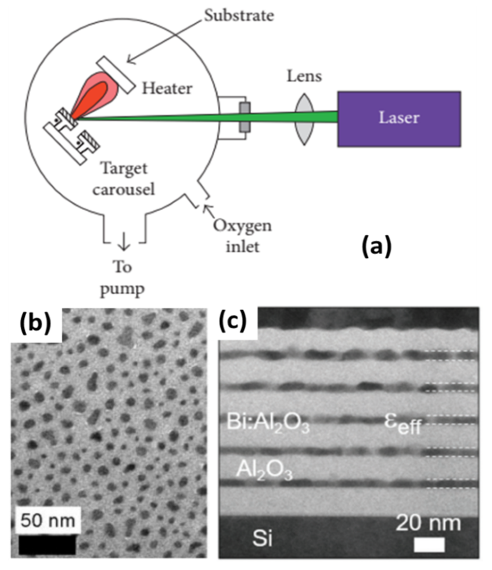
PLD is a laser-assisted method to deposit nanostructures with excellent crystalline quality [32,65]. Typically, PLD is carried out in a vacuum chamber where a laser beam is used to vaporize or ablate Bi from a target, and then the products are collected on a substrate, as shown in Figure 5a, and the Bi thin films or Bi nanoparticles embedded in, e.g., the Al2O3 matrix (Figure 5b,c), are obtained [55,60]. It is a challenge for PLD to fully control the shape and size distribution of, e.g., the Bi nanoparticles (Figure 5b). However, for broadband applications, the negative influences of the poor size and shape control seem unimportant. Active analog phase tuning [55], high-transmission-contrast thermo-optical response [58], and some other applications have been successfully demonstrated in PLD-prepared Bi metamaterials.
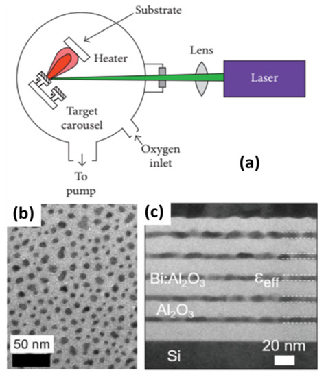
Figure 5.
(a) Scheme illustration of the PLD process(reprinted with permission from [32] © 2018, under CC BY 4.0 license); transmission electron microscope (b) plane-view(reprinted with permission from [60] © 2013, Springer), and (c) cross-section micrographs of Al2O3/BiNPs/Al2O3 thin films(reprinted with permission from © 2020, De Gruyter, under CC BY license).
GLAD exploits the inherent line-of-sight coating principle of PVD systems along with shadowing to achieve quasi-3D nanosized columnar fills (NRs)with an intrinsic tilt and porosity (Figure 6a) [66,67]. As a catalyst-free process with a wafer-scale fabrication, broad source-material feasibility, as well as good size and shape controllability, it is used to produce large-scale and densely packed Bi nanorod arrays with high aspect-ratio (Figure 6b) [66], which could serve as the linearly thermally tunable metamaterial [57].
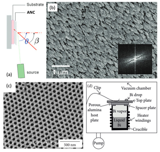
Figure 6.
(a) Schematic illustration of the GLAD process for anisotropic nano column (ANC) arrays; (b) scanning electron microscopy (SEM) of ANC of Bi prepared by GLAD method (reprinted with permission from [67] © 2014, IOP); (c) SEM image of AAO template (reprinted with permission from [32] © 2018 under CC BY 4.0 license); and the (d) Schematic illustration of the template-assisted vapor deposition (reprinted with permission from [32] © 2018 under CC BY 4.0 license).
AAO template-assisted deposition is a cost-effective method to prepare the ordered nanostructure without using a lithography technique [32]. As the host material with a uniform porous structure (Figure 6c), by tuning the anodization parameters, the pore diameter and packing density of AAO can be well controlled. In such AAO templates, arrays of Bi nanorods were grown by filling the pores through vapor deposition (Figure 6d), or alternatively, pressurized injection and electrochemical deposition [32,34,68]. As such, the ordered bismuth enhanced plasmonic nanorods desired for selectivity color filters might be prepared by a simple lithography-free AAO + PVD route [53].
4. Functional Devices Based on Bismuth Metamaterials for Light Manipulation
In earlier years, bismuth was studied due to its great potential in thermal power devices, magnetoresistance, quantum oscillation, superconductors, etc., as mentioned above. Recently, the valuable optical properties of bismuth has inspired the emergence of several functional meta-devices, such as broadband absorbers [49], high selectivity color filters [53,55], active transmission switches and analog phase tuners [54,55].
4.1. Light Absorber
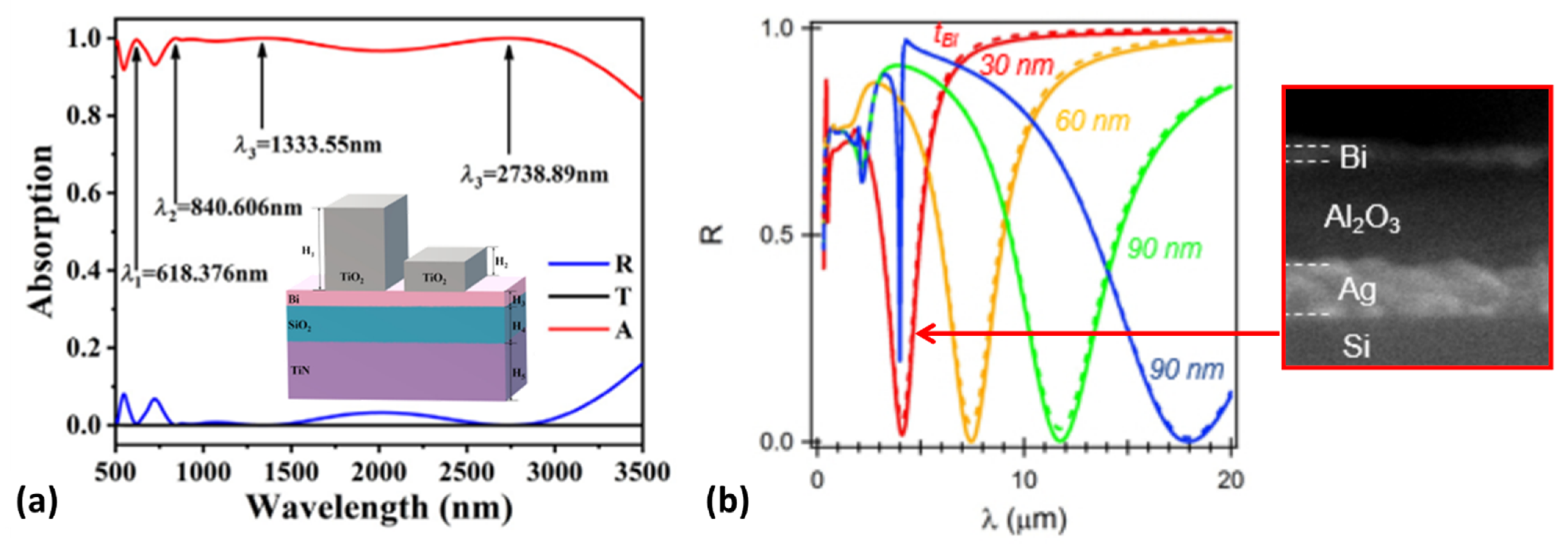
Metamaterial-based perfect absorbers can be employed in various applications. While these narrowband absorbers are of great interest for sensing and spectroscopy applications, several other areas, such as photovoltaic and thermal-photovoltaic steam generation and photodetection, require spectral broadness [22]. However, conventional designs based on noble metals cover a part of the visible or NIR spectrum and their absorption bandwidths (BW) are inherently restricted [49]. Using lithography-free multilayer planar perfect absorbers made of bismuth insulator pairs is a very attractive method to obtain very-near-perfect broadband absorbers with >90% absorption for incident light in an wide regime spanning from 510 nm to 2510 nm [49]. Moreover, metal–insulator pairs with a modified TiO2 nano-column resonator can be used to design absorbers with an average absorption of higher than 90% in the wavelength range of 500 to 3500 nm and greater than 99% in the wavelength range of 811 to 3162 nm (Figure 7a) [45]. Furthermore, thanks to the co-contribution of guided mode resonance, cavity resonance and surface-plasmon resonance, an absorber composed of a dielectric film and a phase-change material film sandwiched between a bismuth square ring array and a continuous bismuth mirror can further extend its high absorption to an even wider range (400–4000 nm, >94% at all wavelengths and averagely >97%) [47]. Aside from the bismuth meta-absorber in the Vis–NIR regime, due to the strong Mie resonance in MIR–FIR range, tunable perfect absorption by a sub-λ/100 bismuth nano-film in a fractal phasor resonant cavity was developed and demonstrated angle-insensitive perfect absorption at a variable wavelength from 3 to 20 μm (Figure 7b) [50]. Alternatively, polarization insensitivity can be also enhanced by wide-angle high absorption [51]. The absorber is composed of an ultra-thin Bi film and a continuous metallic film separated by a dielectric spacer, exhibiting narrowband absorption that can continuously span the whole MWIR range from 3 to 6 μm by varying the geometric parameters. In addition to the Bi-film-based absorber, a bismuth-based helical metamaterial surface has also been suggested as the dual-band Vis-IR absorber [52], and the GLAD technique is a promising method to prepare such helical structure without needing lithography [69].

Figure 7.
(a) Wideband absorber based on Bi metamaterial; (b) Perfect absorption at high refractive index resonances of Bi nanolayers tunable over the mid-to-far infrared by adjusting the thickness of Bi nanolayer tBi. (reprinted with permission from [50] © 2018 under CC BY 4.0 license).
4.2. Color Filter
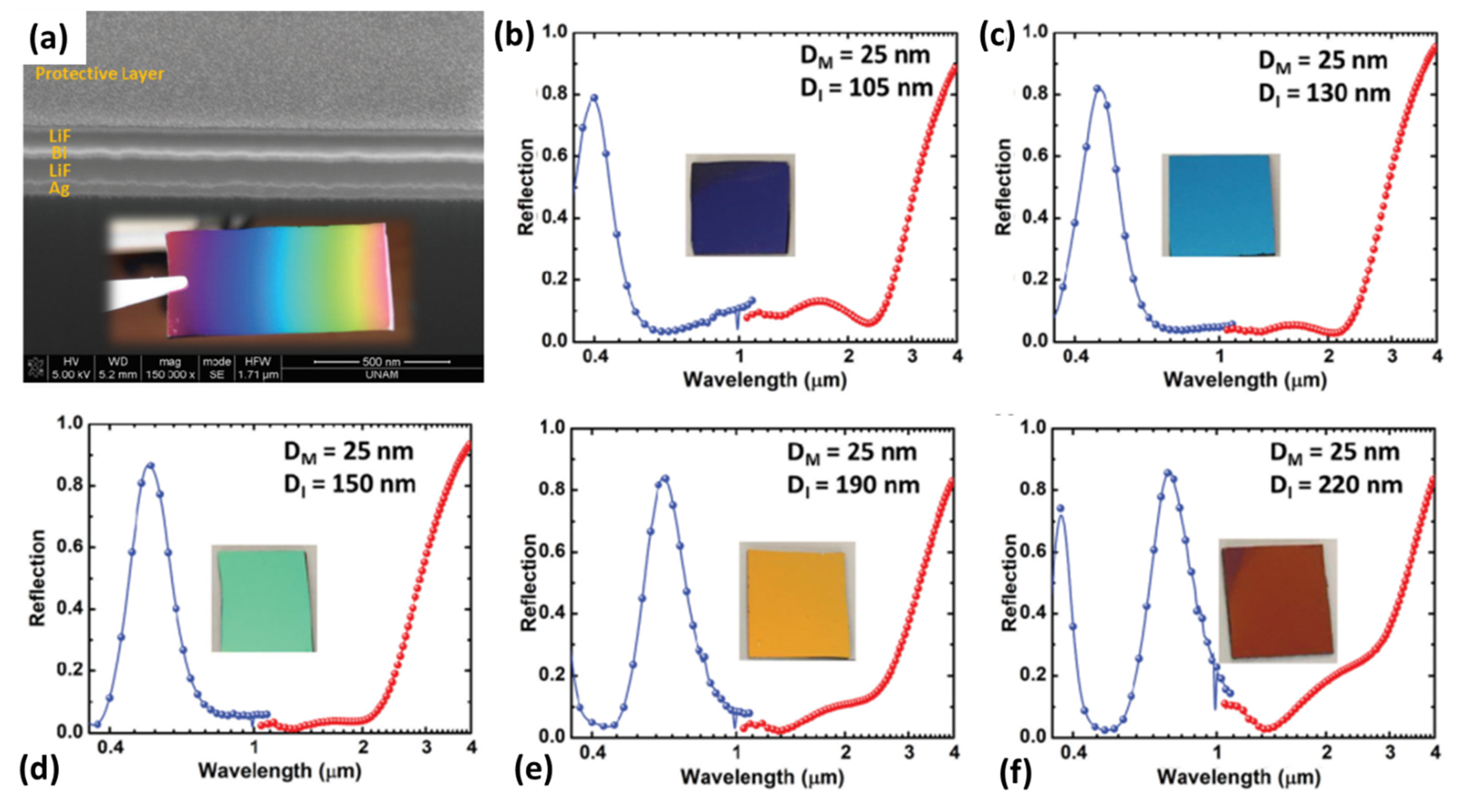
Color filtering is another attractive function of Bi metamaterials. The Bi-based metal–insulator pairs (Figure 8a), besides being used as a wide-band absorber, could also be an excellent color filter since it exhibits a narrow-band high-amplitude reflective response at a shorter wavelength value (Figure 8b–f) [49]. Moreover, a specifically designed filter based on Bi nanostructures was also proposed and showed high color selectivity [53]. Combining the characteristics of metal–insulator–metal (MIM) cavities and nanorod array structures, the proposed filter based on the metal nanorod array structure has been proposed, using bismuth (Bi) as the reflective layer. Other than the traditional nanometal materials, the dielectric constant of bismuth can match the ideal conditions of light absorption. As such, the filter shows reflectivity as high as 95% in a specific wavelength range and has a narrow bandwidth [53]. Its highly selective filtering effects on the Vis–NIR bands allow it to be used as a reflective color filter with >90% reflection for all RGB (red, green, and blue) colors. The position of the reflective resonance peak can be adjusted by changing the thickness of the intermediate layer with a high spectra resolution and easy modulation feasibility. Due to the narrow spectral bandwidth of the proposed device, the problem of crosstalk between the generated colors can be well-solved by the highly color-selective design [53]. Consequently, the color filter based on the Bi meta material could be very promising to image sensing, photoelectric detection, and smart displays.
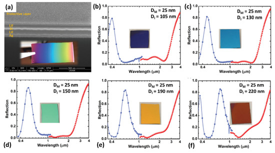
Figure 8.
(a) The cross-sectional SEM image of the fabricated color filter based on Bi metamaterial composed of Ag-LiF-Bi-LiF MIMI cavity, and the inset shows a monolithically designed spatially variant color filter by linear variation of the insulator thickness across the sample, by adjusting the geometrical parameters of the deposition system; the normal incident absorption spectra (wavelength from 0.35 to 4 μm) of the cavity with a fixed optimal Bi layer thickness of 25 nm but different LiF thickness of (b) 105 nm (blue), (c) 130 nm (cyan), (d) 150 nm (green), (e) 190 nm (orange), and (f) 220 nm (red). In all the measurements in Figure 8b–f, blue lines correspond to the spectra from 0.35 to 1.1 μm probed by in-house optical microscopy consisting with halogen lamp and spectrometer, while the spectra from 1 to 4 μm (red lines) is detected by the Fourier-transform infrared spectroscopy (FTIR) system (reprinted with permission from [49] © 2019 under CC BY 4.0 license).
Besides the multilayer cavity structure, color-filtering can be also achieved in the bismuth nanoparticle system. Yu-Peng Chen et al. artfully combined thermodynamic and kinetic features of the thermal evaporation process to fabricate core–shell bismuth nanoparticles with various sizes of bismuth on a large-area silicon substrate by using a one-step thermal evaporation deposition method. In this system, at 12 different sites of the fabricated sample from center to edge (illustrated in Figure 9a), varied colors are shown (Figure 9b), which almost cover the full visible color spectrum in a hue order with a color gamut that is close to sRGB, as shown Figure 9c [62]. The eye-view optical microscopies conform very well with the reflection spectra and the numerical simulations (Figure 9d), indicating the great potential of the nanoparticle system to construct Bi metamaterials with lithography-free fabrication methods.
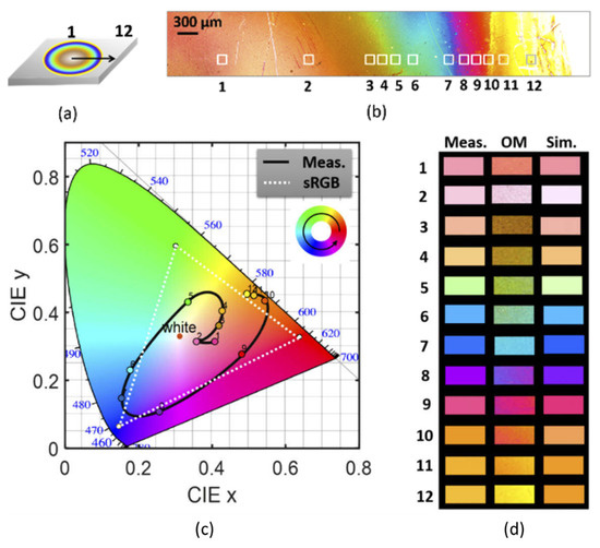
Figure 9.
(a) Indication of section order on the fabricated sample from center to edge. (b) Optical microscopy image of the fabricated Bi nanoparticles and the indication of the 12 section indexes. (c) Comparison of the CIE color gamut of the fabricated Bi NPs converted from measured reflection spectra with sRGB. (d) The corresponding color palettes on the CIE diagram of the measured spectra (Meas.), measured OM images (OM), and of the simulated spectra (Sim.) of the fabricated Bi NPs at the featured 12 sections. (reprinted with permission from [62] © 2020 Optics Society of America under CC BY 4.0 license).
4.3. Thermo-Optical Devices
Besides the use of passive bismuth metamaterials such as in perfect absorbers and color filters, as discussed in Section 4.1 and Section 4.2, some interest has also been devoted to the active metamaterials whose optical responses can be tuned reversibly in the desired spectral range by external stimulation [58,60]. Especially, Bi has the capability of displaying interband plasmonic effects in the near-ultraviolet-to-near infrared range and shows a relatively low melting point at 273.1 °C [40,43]. Therefore, nanostructures made of bismuth metals could be quite interesting building blocks for thermo-optical devices based on the optical contrast between their solid and liquid phases [54]. The typical thermo-optical component is built using bismuth nanoparticles embedded in dielectric media such as germinate glasses or alumina [41,55,60]. Such a structure can be thermally switched, and exhibits transmission–temperature hysteresis loops, as shown in Figure 10a [59]. It was found that a wavelength of λ = 560 nm in the heating–cooling cycles causes the transmission of the Bi NP embedded in Al2O3 media to abruptly increase (decrease) during heating (cooling), which corresponds to the melting (solidification) of Bi nanostructures. Moreover, the thermal configuration of Bi NP is diameter-dependent, which is a well-known nano size effect existing in several other metal nanostructures as well [70]. Furthermore, the optical contrast of Bi in its liquid and solid state varies at different wavelength regimes (Figure 10b) [58], e.g., the melting(around 320 °C) of BiNP in germinate glass production sharply increases transmission for λ < 600 nm but decreases transmission for λ > 600 nm. Meanwhile, at solidification around 90 °C, transmission decreases for λ < 600 nm and increases for λ > 600 nm. Such contrasting transmission changes can be ascribed to the different dispersive properties of solid and liquid Bi, respectively, at short- and long-wavelength regimes [40,43], which relates to thermal-induced polaritonic-to-plasmonic transition [54].
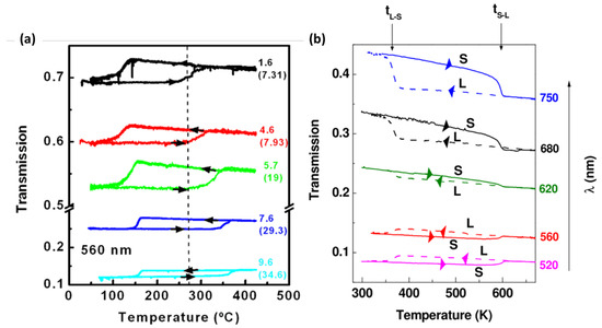
Figure 10.
(a) Optical transmission of the Bi nanoparticles with different mean Feret diameters embedded in Al2O3 thin films of Bi at a wavelength of 560 nm controlled by heating-cooling cycles (here the arrows → mark the heating process and the arrows ← mark the cooling process) (reprinted with permission from [59] @ AIP); and (b) wavelength-dependent transmission–temperature hysteresis loops of active Bi metamaterials (reprinted with permission from [58] @ Elsvier).
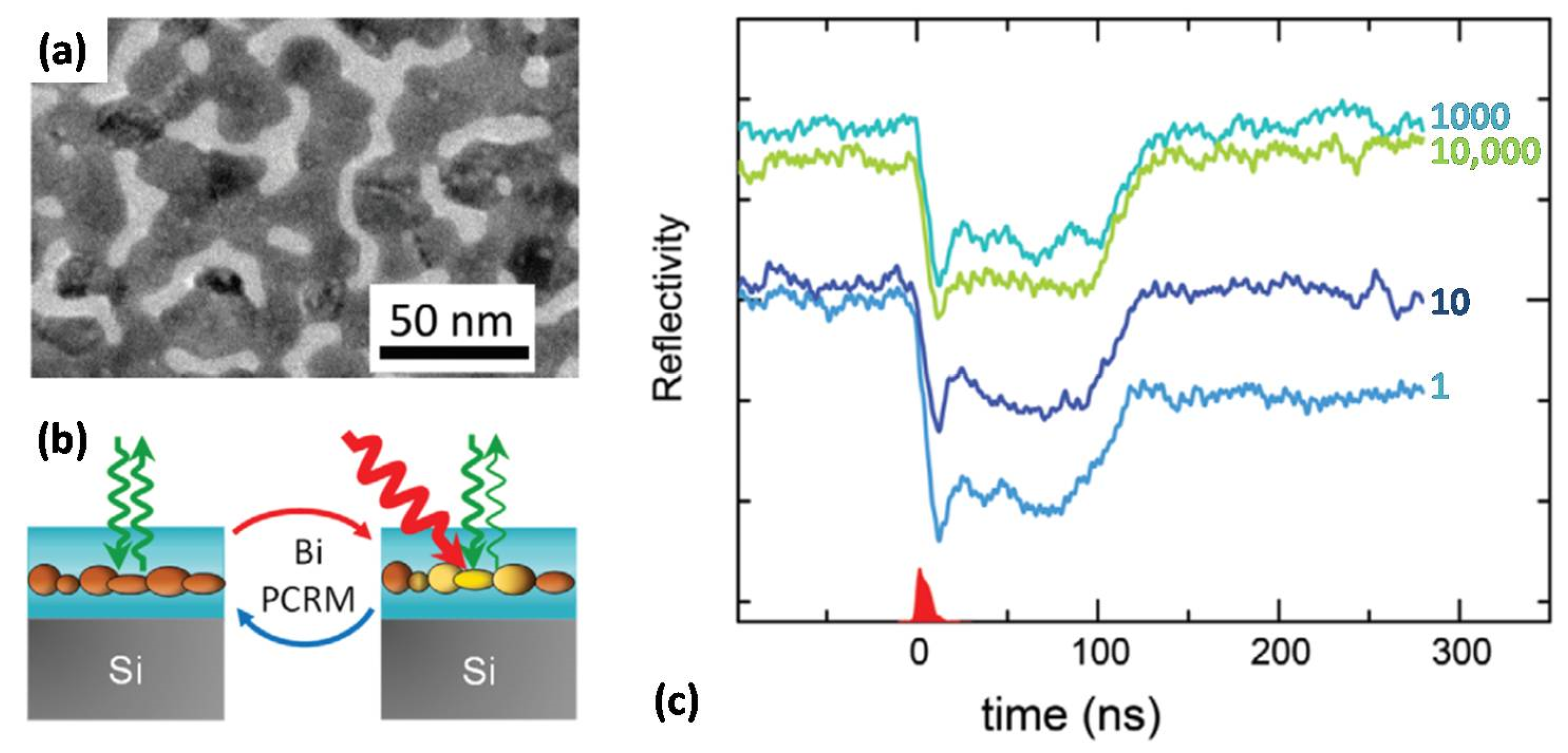
The temporal response to the thermal switching of the Bi metamaterial can be probed by observing the dynamic behavior of the meting-solidification process stimulated by a nanosecond laser [56]. Miguel et al. presented phase-change random metasurfaces based on Bi nano particles embedded in anAl2O3matrix (Figure 11a) [56]. In this system, the nanosecond laser could smoothly tune the solid–liquid–solid phase-change cycle under laser irradiation, with an operation time window from 10 to 700 ns, by adjusting the laser fluence according to real-time monitoring of its reflectivity (Figure 11b). This work revealed for the first time crucial, yet unexplored, temporal solid–liquid phase change dynamics of Bi-based random metasurfaces (i.e., lithography free) upon nanosecond laser irradiation, compared to using a conventional furnace as the thermal heater with a low speed and much higher energy cost. Moreover, it was found that the fast optical switching process is highly repeatable (more than 10,000 cycles, Figure 11c), showing the robustness of the laser-induced process. As such, employing an ultrashort laser to trigger the phase change could facilitate the integration of fast nanophotonic switching devices based on Bi metamaterial.
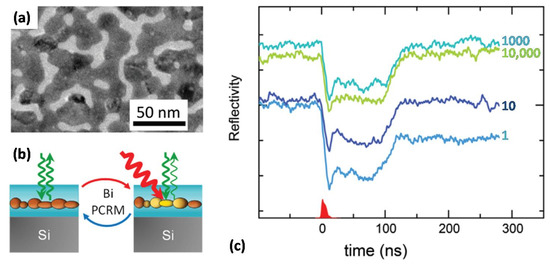
Figure 11.
(a) TEM plan-view image of typical phase-change random metasurfaces based on Bi nano particles embedded in anAl2O3 matrix; (b) illustration of the reversible process undergone by the sample surface upon excitation with the nanosecond laser (red) that was monitored in real time with a continuous-wave laser beam (green, probe); and (c) reflectivity transients measured upon irradiation of the same area of the sample with up to 10,000 pulses at constant fluence. (reprinted with permission from [56] © 2022 Willey under CC BY license).
The aforementioned transmission modulation reflects the image-part change in the effective refractive index due to the solid–liquid phase-change in the Bi metamaterial, and such modulation could also occur in phase-tuning considering the Kramers–Kronig relationship which couples the real-part and image-part change in the effective refractive index. Still, in the system of Bi particles embedded in Al2O3, the maximum phase-tuning of 320° (1.8 π) can be obtained at 230 °C by fully melting all of the Bi particles (Figure 12a,b) [55,71]. After cooling down to 25 °C, the Bi NPs return to their initial solid state, thus demonstrating the fully reversible phase tuning. Similarly to the transmission–temperature hysteresis proposed above, the under-cooling of the Bi metasurface enables the phase-temperature hysteretic response, which leaves the analog-tuned phase stable over a temperature range of about 100 °C, and accordingly endows the Bi metasurface with semi-volatile optical memory capabilities [55].
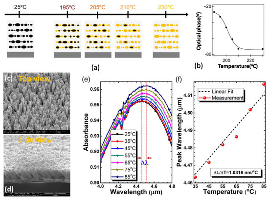
Figure 12.
(a) Temperature-controlled partial melting of Bi nanostructures (reprinted with permission from [55] © 2020 under CC BY 4.0 license); (b) this enables the analog tuning of the optical phase reflected by a Bi-based metamaterial (reprinted with permission from [55] © 2020 under CC BY 4.0 license); (c) top view and (d) side view of densely packed Bi nanorods prepared by the GLAD method(reprinted with permission from [57] © 2020 Wiley); (e) the spectral absorption peak resonance wavelength change in the fabricated device as a function of temperature (reprinted with permission from [57] © 2020 Wiley), and (f) the estimated thermal-optical sensitivity through the linear fitting of the data(reprinted with permission from [57] © 2020 Wiley).
Besides the hysteresis response due to the solid–liquid phase-change of the Bi nanostructures, non-hysteretic tuning can also be thermally implemented in the Bi metamaterial, at a relatively low temperature range (25–85 °C). Mahmut et al. presented the disordered Bi nanorods prepared by the GLAD technique as a linearly thermally tunable metamaterial (Figure 12c,d) [57]. In this system, the linear red shift of the resonance at the MIR-to-FIR range (2–10 μm) was observed with increasing temperature, as shown in Figure 12e. The high thermo-optical sensitivity coefficient of ~1 nm/°C (Figure 12f) may have originated from the deep subwavelength light confinement, and the dispersion of the energy band, of the Bi nanorods [57]. Such a simple but robust and easy-to-fabricate device might be quite promising for applications such as thermo-optic modulators [72], switches [73], and infrared camouflage [27].
4.4. Other Applications
Several other applications have been proposed recently for Bi metamaterials. The use of Bi thin films and nanorods as the active medium in photodetectors has been proposed [74,75,76], thanks to their broadband absorption of light as mentioned above, and excellent conduction properties involving surface states. It is also quite apparent that these features could be promising in solar-cell-based energy harvesting. Additionally, some nanostructures of bismuth, despite their small nearfield enhancement, allow enhancement of Raman signals. All these reports on the properties of bismuth, beside its applications as alight absorber, color filter and switching device, strongly imply the potential of bismuth metamaterials in areas beyond those that we have discussed in this paper.
5. Conclusions and Perspective
Over the past decades, bismuth has gained the interest of scientists due to its promising thermoelectricity, quantum confinement and finite size effects and enhanced magnetoresistance. In recent years, increasing interest has been further extended to its peculiar optoelectronic properties. Bismuth optical metamaterial can manipulate the light over extremely wide wavelength ranges with various functions, from absorbing to filtering and switching. Moreover, Bi metamaterials can be fabricated without complicated and expensive lithographic processes, which makes it beneficial due to its cost-effectiveness and scalable production. In this article, we have presented a comprehensive review of the recent advances in this field; notably, the electrical and optical properties of Bi, the lithography-free fabrication of Bi metamaterials, and emerging functional devices for light manipulation. Bismuth can support the scope of optical resonance from the UV to FIR and THz range: (1) Interband plasmonic resonance in the UV–Vis regime due to the rich electron bands in bismuth as well as their strong inter band transition; (2) Mie resonance in the SWIR and MWIR originate from the very high ε1 around 100, and the non-zero but lower ε2 of 20~40 in this region, thanks to its great compositional ε tailoring; and the (3) “free-carrier” plasmonic resonance at the FIR to THz range produced by the low-density free-carrier within. Utilizing such unique optical response, several functional metamaterials have been developed, from narrowband reflective color filters to extremely broadband near-perfect absorbers and transmission switching, as well as analog phase tuners. Moreover, these Bi metamaterials are fabrication-friendly without relying on complicated lithography techniques, but employ the more cost-effective PVD, PLD, and GLAD, as well as the possibility of its combination with templates such as AAO.
Preferable optical properties and a good fabrication feasibility allow Bi meta materials to be adapted to a series of optical and optoelectronic applications as mentioned above, but a better-controlled crystalline quality, nanostructure size and shape distribution, and environmental uniformity, are still highly desired [21,33,34,50]. Moreover, beyond the known materials based on Bi, there are probably other compositions which enable better properties such as lower plasmonic losses. These physical qualities warrant the further exploration of the so called “Giant interband materials” family [71]. Thanks to the singular-band structure of Bi and the related “Giant interband materials”, the bulky and/or nano-dimension metamaterials based on these systems with improved quality are promising to the development on light manipulation. In addition, although many significant optical behaviors of Bi metamaterials can be qualitatively explained by classical modeling, several works have also implied that quantum confinement effects should be carefully considered with the corresponding modification on their classical dielectric features [32,71]. Especially when the size of a nanostructure becomes small enough (typically, remarkably smaller than the free-charge carrier mean-free path of Bi at a few μm) [33], its electronic structure (and thus its dielectric function) can change from that of the bulky structure and become size-dependent. Such size-shrinking-induced confinement effects are able to trigger semimetal–semiconductor transitions [77,78,79]. The confined semiconductive opens an increasing bandgap Eg upon a decrease in the structure size [80]. Accordingly, strong blueshifts in the optical absorption occur, agreeing well with the electron energy-loss spectra [81]. Quantum-confined Bi nanostructures might be beneficial to produce broadband optical-absorbing devices with an ultra-small footprint because of the more suitable spectral dependence of their ε [71] compared with structures without such confinement effects. Therefore, the quantum phenomena of Bi nanostructures would be quite valuable to provide more clues to further improve Bi metamaterials for light manipulation in the future.
In summary, progression in the lithography-free fabrication of Bi metamaterials, the control and understanding of their excellent optical responses, and the emergence of functional devices open new possibilities for Bi metamaterials beyond the already-explored paths. More experimental observations are needed to dig up its optical potential. Further developments are also necessary to overcome the obstacles and reveal unsolved issues to achieve the production of more practical Bi metamaterials and related devices.
Author Contributions
Conceptualization, Z.L. and L.Z.; writing—original draft preparation, Z.L.; writing—review and editing, Y.T. and L.Z. All authors have read and agreed to the published version of the manuscript.
Funding
This research was supported by Hunan Provincial Natural Science Fund (2019JJ50025), the Scientific Research Fund of Hunan Provincial Education Department (No. 20C0367, No. 19B100), and Hunan Provincial Philosophy and Social Science Foundation (21YBA176).
Institutional Review Board Statement
Not applicable.
Informed Consent Statement
Not applicable.
Data Availability Statement
All data included in this study are available upon request by contact with the corresponding author.
Conflicts of Interest
The authors declare no conflict of interest.
References
- Liu, Y.; Zhang, X. Metamaterials: A new frontier of science and technology. Chem. Soc. Rev. 2011, 40, 2494–2507. [Google Scholar] [CrossRef]
- Turpin, J.P.; Bossard, J.A.; Morgan, K.L.; Werner, D.H.; Werner, P.L. Reconfigurable and Tunable Metamaterials: A Review of the Theory and Applications. Int. J. Antennas Propag. 2014, 2014, 429837. [Google Scholar] [CrossRef]
- Li, H.; Zhou, H.; Wei, G.; Xu, H.; Qin, M.; Liu, J.; Wu, F. Photonic spin-selective perfect absorptance on planar metasurfaces driven by chiral quasi-bound states in the continuum. Nanoscale 2023, 15, 6636–6644. [Google Scholar] [CrossRef] [PubMed]
- Yang, K.; Wang, J.; Yao, X.; Lyu, D.; Zhu, J.; Yang, Z.; Ren, B. Large-Area Plasmonic Metamaterial with Thickness-Dependent Absorption. Adv. Opt. Mater. 2021, 9, 2001375. [Google Scholar] [CrossRef]
- Harvey, E.; Ghantasala, M. 12—Nanofabrication. In Nanostructure Control of Materials; Hannink, R.H.J., Hill, A.J., Eds.; Woodhead Publishing: Sawston, UK, 2006; pp. 303–330. [Google Scholar]
- Wang, S.; Zhou, Z.; Li, B.; Wang, C.; Liu, Q. Progresses on new generation laser direct writing technique. Mater. Today Nano 2021, 16, 100142. [Google Scholar] [CrossRef]
- Vazquez-Mena, O.; Gross, L.; Xie, S.; Villanueva, L.G.; Brugger, J. Resistless nanofabrication by stencil lithography: A review. Microelectron. Eng. 2015, 132, 236–254. [Google Scholar] [CrossRef]
- Han, M.; Lee, W.; Lee, S.K.; Lee, S.S. 3D microfabrication with inclined/rotated UV lithography. Sens. Actuators A Phys. 2004, 111, 14–20. [Google Scholar] [CrossRef]
- Groves, T.R.; Pickard, D.; Rafferty, B.; Crosland, N.; Adam, D.; Schubert, G. Maskless electron beam lithography: Prospects, progress, and challenges. Microelectron. Eng. 2002, 61–62, 285–293. [Google Scholar] [CrossRef]
- Ali, M.Y.; Hung, W.; Yongqi, F. A review of focused ion beam sputtering. Int. J. Precis. Eng. Manuf. 2010, 11, 157–170. [Google Scholar] [CrossRef]
- Caruana, A.; Cropper, M.; Stanley, S. Spontaneous growth of bismuth nanowires on a sputter-deposited thin bismuth film. Surf. Coatings Technol. 2015, 271, 8–12. [Google Scholar] [CrossRef]
- Huang, J.; Kim, F.; Tao, A.R.; Connor, S.; Yang, P. Spontaneous formation of nanoparticle stripe patterns through dewetting. Nat. Mater. 2005, 4, 896–900. [Google Scholar] [CrossRef] [PubMed]
- Barranco, A.; Borras, A.; Gonzalez-Elipe, A.R.; Palmero, A. Perspectives on oblique angle deposition of thin films: From fundamentals to devices. Prog. Mater. Sci. 2016, 76, 59–153. [Google Scholar] [CrossRef]
- Wang, S.; Zhang, Y.; Wang, W.; Li, G.; Ma, X.; Li, X.; Zhang, Z.; Qian, Y. Template-assisted synthesis of porous molybdenum dioxide nanofibers and nanospheres by redox etching method. J. Cryst. Growth 2006, 290, 96–102. [Google Scholar] [CrossRef]
- Selimis, A.; Mironov, V.; Farsari, M. Direct laser writing: Principles and materials for scaffold 3D printing. Microelectron. Eng. 2015, 132, 83–89. [Google Scholar] [CrossRef]
- Toudert, J. Spectrally Tailored Light-Matter Interaction in Lithography-Free Functional Nanomaterials. Phys. Status Solidi (a) 2019, 217, 1900677. [Google Scholar] [CrossRef]
- Barnes, W.L.; Dereux, A.; Ebbesen, T.W. Surface plasmon subwavelength optics. Nature 2003, 424, 824–830. [Google Scholar] [CrossRef] [PubMed]
- Yu, W.; Tian, Y.; Zhang, S.; Tan, W. Arbitrary power-splitting-ratio achieved in 1×2 hybrid plasmonic multimode inter-ference device by structure symmetry broken. Optik 2020, 220, 165141. [Google Scholar] [CrossRef]
- Tian, Y.; Zhang, S.; Tan, W. An Ultra-Compact Design of Plasmonic Memristor with Low Loss and High Extinction Effi-ciency Based on Enhanced Interaction between Filament and Concentrated Plasmon. Photonics 2021, 8, 437. [Google Scholar] [CrossRef]
- Campos, A.; Troc, N.; Cottancin, E.; Pellarin, M.; Weissker, H.C.; Lermé, J.; Hillenkamp, M. Plasmonic quantum size effects in silver nanoparticles are dominated by interfaces and local environments. Nat. Phys. 2019, 15, 275–280. [Google Scholar] [CrossRef]
- Tian, Y.; Jiang, L.; Deng, Y.; Deng, S.; Zhang, G.; Zhang, X. Bi-nanorod/Si-nanodot hybrid structure: Surface dewetting induced growth and its tunable surface plasmon resonance. Opt. Mater. Express 2015, 5, 2655–2666. [Google Scholar] [CrossRef]
- Ghobadi, A.; Hajian, H.; Butun, B.; Ozbay, E. Strong Light–Matter Interaction in Lithography-Free Planar Metamaterial Perfect Absorbers. ACS Photon. 2018, 5, 4203–4221. [Google Scholar] [CrossRef]
- Amin, R.; Maiti, R.; Carfano, C.; Ma, Z.; Tahersima, M.H.; Lilach, Y.; Ratnayake, D.; Dalir, H.; Sorger, V.J. 0.52 V mm ITO-based Mach-Zehnder modulator in silicon photonics. APL Photon. 2018, 3, 126104. [Google Scholar] [CrossRef]
- Le, K.Q. ITO-based electro-optical modulator integrated in silicon-on-insulator waveguide using surface plasmon interference. Phys. B Condens. Matter. 2021, 602, 412313. [Google Scholar] [CrossRef]
- Guler, U.; Shalaev, V.M.; Boltasseva, A. Nanoparticle plasmonics: Going practical with transition metal nitrides. Mater. Today 2014, 18, 227–237. [Google Scholar] [CrossRef]
- Agarwal, A.; Vitiello, M.S.; Viti, L.; Cupolillo, A.; Politano, A. Plasmonics with two-dimensional semiconductors: From basic research to technological applications. Nanoscale 2018, 10, 8938–8946. [Google Scholar] [CrossRef] [PubMed]
- Ghobadi, A.; Ghobadi, T.G.U.; Ozbay, E. Lithography-free metamaterial absorbers: Opinion. Opt. Mater. Express 2022, 12, 524–532. [Google Scholar] [CrossRef]
- Schindler, F.; Wang, Z.; Vergniory, M.G.; Cook, A.M.; Murani, A.; Sengupta, S.; Kasumov, A.Y.; Deblock, R.; Jeon, S.; Drozdov, I.; et al. Higher-order topology in bismuth. Nat. Phys. 2018, 14, 918–924. [Google Scholar] [CrossRef]
- Huber, T.; Nikolaeva, A.; Gitsu, D.; Konopko, L.; Graf, M. Quantum confinement and surface-state effects in bismuth nanowires. Phys. E: Low-Dimens. Syst. Nanostruct. 2007, 37, 194–199. [Google Scholar] [CrossRef]
- Yang, H.; Fauqué, B.; Malone, L.; Antunes, A.B.; Zhu, Z.; Uher, C.; Behnia, K. Phase diagram of bismuth in the extreme quantum limit. Nat. Commun. 2010, 1, 47. [Google Scholar] [CrossRef]
- Yokota, K.; Takeda, J.; Dang, C.; Han, G.; McCarthy, D.N.; Nagao, T.; Hishita, S.; Kitajima, M.; Katayama, I. Surface metallic states in ultrathin Bi(001) films studied with terahertz time-domain spectroscopy. Appl. Phys. Lett. 2012, 100, 251605. [Google Scholar] [CrossRef]
- Tian, Y.; Toudert, J. Nanobismuth: Fabrication, Optical, and Plasmonic Properties—Emerging Applications. J. Nanotechnol. 2018, 2018, 3250932. [Google Scholar] [CrossRef]
- Shim, W.; Ham, J.; Lee, K.-I.; Jeung, W.Y.; Johnson, M.; Lee, W. On-Film Formation of Bi Nanowires with Extraordinary Electron Mobility. Nano Lett. 2008, 9, 18–22. [Google Scholar] [CrossRef] [PubMed]
- Kim, J.; Shim, W.; Lee, W. Bismuth nanowire thermoelectrics. J. Mater. Chem. C 2015, 3, 11999–12013. [Google Scholar] [CrossRef]
- Yang, F.Y.; Liu, K.; Hong, K.; Reich, D.H.; Searson, P.C.; Chien, C.L. Large Magnetoresistance of Electrodeposited Sin-gle-Crystal Bismuth Thin Films. Science 1999, 284, 1335–1337. [Google Scholar] [CrossRef]
- Huber, T.E.; Celestine, K.; Graf, M.J. Magnetoquantum oscillations and confinement effects in arrays of 270-nm-diameter bismuth nanowires. Phys. Rev. B 2003, 67, 245317. [Google Scholar] [CrossRef]
- Li, L.; Checkelsky, J.G.; Hor, Y.S.; Uher, C.; Hebard, A.F.; Cava, R.J.; Ong, N.P. Phase Transitions of Dirac Electrons in Bismuth. Science 2008, 321, 547–550. [Google Scholar] [CrossRef]
- Liu, Y.; Allen, R.E. Electronic structure of the semimetals Bi and Sb. Phys. Rev. B 1995, 52, 1566–1577. [Google Scholar] [CrossRef]
- Fuseya, Y.; Ogata, M.; Fukuyama, H. Transport Properties and Diamagnetism of Dirac Electrons in Bismuth. J. Phys. Soc. Jpn. 2015, 84, 012001. [Google Scholar] [CrossRef]
- Toudert, J.; Serna, R. Interband transitions in semi-metals, semiconductors, and topological insulators: A new driving force for plasmonics and nanophotonics [Invited]. Opt. Mater. Express 2017, 7, 2299–2325. [Google Scholar] [CrossRef]
- Toudert, J.; Serna, R.; Camps, I.; Wojcik, J.; Mascher, P.; Rebollar, E.; Ezquerra, T.A. Unveiling the Far Infrared-to-Ultraviolet Optical Properties of Bismuth for Applications in Plasmonics and Nanophotonics. J. Phys. Chem. C 2017, 121, 3511–3521. [Google Scholar] [CrossRef]
- Hunderi, O. Optical properties of crystalline and amorphous bismuth films. J. Phys. F: Met. Phys. 1975, 5, 2214. [Google Scholar] [CrossRef]
- Toudert, J.; Serna, R. Ultraviolet-visible interband plasmonics with p-block elements. Opt. Mater. Express 2016, 6, 2434–2447. [Google Scholar] [CrossRef]
- Toudert, J.; Serna, R.; Deeb, C.; Rebollar, E. Optical properties of bismuth nanostructures towards the ultrathin film regime. Opt. Mater. Express 2019, 9, 2924–2936. [Google Scholar] [CrossRef]
- Wang, F.; Fan, H.; Zeng, X. Bismuth-based broadband metamaterial absorber. J. Nanophotonics 2022, 16, 036004. [Google Scholar] [CrossRef]
- Chen, Y.F. Nanofabrication by electron beam lithography and its applications: A review. Microelectron. Eng. 2015, 135, 57–72. [Google Scholar] [CrossRef]
- Wu, J.; Huang, D.; Wu, B.; Wu, X. Extremely broadband light absorption by bismuth-based metamaterials involving hybrid resonances. Phys. Chem. Chem. Phys. 2022, 24, 21612–21616. [Google Scholar] [CrossRef]
- Agarwal, S. Bismuth Based MIM Metamaterial Absorber for Broadband Absorption. In Proceedings of the 2020 6th International Conference on Signal Processing and Communication (ICSC), Noida, India, 5–7 March 2020; pp. 185–187. [Google Scholar]
- Ghobadi, A.; Hajian, H.; Gokbayrak, M.; Butun, B.; Ozbay, E. Bismuth-based metamaterials: From narrowband reflective color filter to extremely broadband near perfect absorber. Nanophotonics 2019, 8, 823–832. [Google Scholar] [CrossRef]
- Toudert, J.; Serna, R.; Pardo, M.G.; Ramos, N.; Peláez, R.J.; Maté, B. Mid-to-far infrared tunable perfect absorption by a sub—λ/100 nanofilm in a fractal phasor resonant cavity. Opt. Express 2018, 26, 34043–34059. [Google Scholar] [CrossRef]
- Xu, Q.; Wen, Z.; Pan, X.; Tan, C.; Zhang, J.; Qiu, Q.; Sun, Y.; Chen, X.; Dai, N.; Chu, J.; et al. Ultra-thin midwavelength infrared absorber using bismuth based planar thin film metamaterials. Appl. Phys. Express 2022, 15, 082005. [Google Scholar] [CrossRef]
- Agarwal, S.; Srivastava, G.; Prajapati, Y.K. Dual band Vis-IR absorber using bismuth based helical metamaterial surface. Opt. Quantum Electron. 2022, 54, 772. [Google Scholar] [CrossRef]
- Su, J.; Mo, X.; Si, G.; Gu, Q.; Jiang, X.; Lv, J. High selectivity color filters based on bismuth enhanced plasmonic nanorods. Opt. Commun. 2021, 490, 126941. [Google Scholar] [CrossRef]
- Cuadrado, A.; Toudert, J.; Serna, R. Polaritonic-to-Plasmonic Transition in Optically Resonant Bismuth Nanospheres for High-Contrast Switchable Ultraviolet Meta-Filters. IEEE Photonics J. 2016, 8, 4801811. [Google Scholar] [CrossRef]
- Garcia-Pardo, M.; Nieto-Pinero, E.; Petford-Long, A.K.; Serna, R.; Toudert, J. Active analog tuning of the phase of light in the visible regime by bismuth-based metamaterials. Nanophotonics 2020, 9, 885–896. [Google Scholar] [CrossRef]
- Alvarez-Alegria, M.; Siegel, J.; Garcia-Pardo, M.; Cabello, F.; Toudert, J.; Haro-Poniatowski, E.; Serna, R. Nanosecond Laser Switching of Phase-Change Random Metasurfaces with Tunable ON-State. Adv. Opt. Mater. 2021, 10, 2101405. [Google Scholar] [CrossRef]
- Soydan, M.C.; Ghobadi, A.; Yildirim, D.U.; Erturk, V.B.; Ozbay, E. Deep Subwavelength Light Confinement in Disordered Bismuth Nanorods as a Linearly Thermal-Tunable Metamaterial. Phys. Status Solidi (RRL)—Rapid Res. Lett. 2020, 14, 2000066. [Google Scholar] [CrossRef]
- de Castro, M.J.; Cabello, F.; Toudert, J.; Serna, R.; Haro-Poniatowski, E. Potential of bismuth nanoparticles embedded in a glass matrix for spectral-selective thermo-optical devices. Appl. Phys. Lett. 2014, 105, 113102. [Google Scholar] [CrossRef]
- de Castro, M.J.; Serna, R.; Toudert, J.; Navarro, J.F.; Haro-Poniatowski, E. Thermo-optical properties of Bi nanoparticles embedded in germanate glasses and alumina thin films. Ceram. Int. 2015, 41, 8216–8222. [Google Scholar] [CrossRef]
- Serna, R.; de Castro, M.J.; Toudert, J.; Haro-Poniatowski, E.; López, J.G. Role of target conditioning on the thermo-optical response of bismuth nanostructures produced by pulsed laser deposition. Appl. Phys. A 2012, 110, 863–867. [Google Scholar] [CrossRef]
- Tian, Y.; Guo, C.F.; Guo, S.; Wang, Y.; Miao, J.; Wang, Q.; Liu, Q. Bismuth nanowire growth under low deposition rate and its ohmic contact free of interface damage. AIP Adv. 2012, 2, 012112. [Google Scholar] [CrossRef]
- Chen, Y.P.; Lai, C.C.; Tsai, W.S. Full-color based on bismuth core-shell nanoparticles in one-step fabrication. Opt. Express 2020, 28, 24511–24525. [Google Scholar] [CrossRef]
- Kumari, L.; Lin, S.-J.; Lin, J.-H.; Ma, Y.-R.; Lee, P.-C.; Liou, Y. Effects of deposition temperature and thickness on the structural properties of thermal evaporated bismuth thin films. Appl. Surf. Sci. 2007, 253, 5931–5938. [Google Scholar] [CrossRef]
- Wu, B.-K.; Lee, H.-Y.; Chern, M.-Y. Bismuth Nanowire Grown Naturally Using a Sputtering System. Appl. Phys. Express 2013, 6, 035504. [Google Scholar] [CrossRef]
- Mihailescu, I.N.; György, E. Pulsed Laser Deposition: An Overview. In International Trends in Optics and Photonics: ICO IV; Asakura, T., Ed.; Springer: Berlin/Heidelberg, Germany, 1999; pp. 201–214. [Google Scholar]
- Tian, Y.; Guo, S.; Liu, Q. Anisotropic nano-column arrays of bismuth and its conductivity. J. Nanosci. Nanotechnol. 2013, 13, 776–780. [Google Scholar] [CrossRef]
- Tian, Y.; Jiang, L.; Zhang, X.; Deng, Y.; Deng, S. Coexistence and competition of surface diffusion and geometric shielding in the growth of 1D bismuth nanostructures and their ohmic contact. Mater. Res. Express 2014, 1, 035034. [Google Scholar] [CrossRef]
- Li, L.; Zhang, Y.; Li, G.; Zhang, L. A route to fabricate single crystalline bismuth nanowire arrays with different diameters. Chem. Phys. Lett. 2003, 378, 244–249. [Google Scholar] [CrossRef]
- Hawkeye, M.M.; Brett, M.J. Glancing angle deposition: Fabrication, properties, and applications of micro- and nanostructured thin films. J. Vac. Sci. Technol. A 2007, 25, 1317–1335. [Google Scholar] [CrossRef]
- Li, H.; Han, P.; Zhang, X.; Li, M. Size-dependent melting point of nanoparticles based on bond number calculation. Mater. Chem. Phys. 2013, 137, 1007–1011. [Google Scholar] [CrossRef]
- Toudert, J. Quantum nanostructures for plasmonics and high refractive index photonics. J. Physics Photon. 2021, 3, 011003. [Google Scholar] [CrossRef]
- Liu, S.; Feng, J.; Tian, Y.; Zhao, H.; Jin, L.; Ouyang, B.; Zhu, J.; Guo, J. Thermo-optic phase shifters based on silicon-on-insulator platform: State-of-the-art and a review. Front. Optoelectron. 2022, 15, 9. [Google Scholar] [CrossRef]
- Tian, Y.; Zhao, Y.; Liu, S.; Li, Q.; Wang, W.; Feng, J.; Guo, J. Scalable and compact photonic neural chip with low learn-ing-capability-loss. Nanophotonics 2022, 11, 329–344. [Google Scholar] [CrossRef]
- Yao, J.D.; Shao, J.M.; Yang, G.W. Ultra-broadband and high-responsive photodetectors based on bismuth film at room temperature. Sci. Rep. 2015, 5, 12320. [Google Scholar] [CrossRef]
- Yao, J.; Zheng, Z.; Shao, J.; Yang, G. Promoting Photosensitivity and Detectivity of the Bi/Si Heterojunction Photodetector by Inserting a WS2 Layer. ACS Appl. Mater. Interfaces 2015, 7, 26701–26708. [Google Scholar] [CrossRef] [PubMed]
- Huber, T.E.; Johnson, S.D.; Belk, J.H.; Hunt, J.H.; Shirvani, K. Charge Transfer and Photocurrent in Interfacial Junctions between Bismuth and Graphene. Phys. Rev. Appl. 2018, 10, 044020. [Google Scholar] [CrossRef]
- Hoffman, C.A.; Meyer, J.R.; Bartoli, F.J.; Di Venere, A.; Yi, X.J.; Hou, C.L.; Wang, H.C.; Ketterson, J.B.; Wong, G.K. Semimetal-to-semiconductor transition in bismuth thin films. Phys. Rev. B 1993, 48, 11431–11434. [Google Scholar] [CrossRef] [PubMed]
- Zhou, G.; Li, L.; Li, G.H. Semimetal to semiconductor transition and thermoelectric properties of bismuth nanotubes. J. Appl. Phys. 2011, 109, 114311. [Google Scholar] [CrossRef]
- Kockert, M.; Mitdank, R.; Moon, H.; Kim, J.; Mogilatenko, A.; Moosavi, S.H.; Kroener, M.; Woias, P.; Lee, W.; Fischer, S.F. Semimetal to semiconductor transition in Bi/TiO2 core/shell nanowires. Nanoscale Adv. 2020, 3, 263–271. [Google Scholar] [CrossRef]
- Wu, B.-K.; Chern, M.-Y.; Lee, H.-Y. Size-controllable synthesis and bandgap modulation of single-layered RF-sputtered bismuth nanoparticles. Nanoscale Res. Lett. 2014, 9, 249. [Google Scholar] [CrossRef]
- Jiang, N.; Su, D.; Spence, J.C.; Zhou, S.; Qiu, J. Volume plasmon of bismuth nanoparticles. Solid State Commun. 2009, 149, 111–114. [Google Scholar] [CrossRef]
Disclaimer/Publisher’s Note: The statements, opinions and data contained in all publications are solely those of the individual author(s) and contributor(s) and not of MDPI and/or the editor(s). MDPI and/or the editor(s) disclaim responsibility for any injury to people or property resulting from any ideas, methods, instructions or products referred to in the content. |
© 2023 by the authors. Licensee MDPI, Basel, Switzerland. This article is an open access article distributed under the terms and conditions of the Creative Commons Attribution (CC BY) license (https://creativecommons.org/licenses/by/4.0/).


