Article

Method and Installation for Efficient Automatic Defect Inspection of Manufactured Paper Bowls

1
School of Mathematics and Information Engineering, Longyan University, Longyan 364012, China
2
Department of Electronic and Computer Engineering, Tamkang University, New Taipei City 251301, Taiwan
3
School of Resource Engineering, Longyan University, Longyan 364012, China
4
College of Artificial Intelligence, Yango University, Fuzhou 350015, China
5
Department of Chemical and Materials Engineering, National University of Kaohsiung, Kaohsiung 811, Taiwan
6
Department of Aeronautical Engineering, Chaoyang University of Technology, Taichung 413, Taiwan
*
Authors to whom correspondence should be addressed.
Photonics 2023, 10(6), 686; https://doi.org/10.3390/photonics10060686
Submission received: 2 May 2023 / Revised: 5 June 2023 / Accepted: 12 June 2023 / Published: 14 June 2023
(This article belongs to the Special Issue Advanced Photonics Sensors, Sources, Systems and Applications)

Abstract

:
Various techniques were combined to optimize an optical inspection system designed to automatically inspect defects in manufactured paper bowls. A self-assembled system was utilized to capture images of defects on the bowls. The system employed an image sensor with a multi-pixel array that combined a complementary metal-oxide semiconductor and a photo detector. A combined ring light served as the light source, while an infrared (IR) LED matrix panel was used to provide constant IR light to highlight the outer edges of the objects being inspected. The techniques employed in this study to enhance defect inspections on produced paper bowls included Gaussian filtering, Sobel operators, binarization, and connected components. Captured images were processed using these technologies. Once the non-contact inspection system’s machine vision method was completed, defects on the produced paper bowls were inspected using the system developed in this study. Three inspection methods were used in this study: internal inspection, external inspection, and bottom inspection. All three methods were able to inspect surface features of produced paper bowls, including dirt, burrs, holes, and uneven thickness. The results of our study showed that the average time required for machine vision inspections of each paper bowl was significantly less than the time required for manual inspection. Therefore, the investigated machine vision system is an efficient method for inspecting defects in fabricated paper bowls.

1. Introduction

Previous research has shown that in Taiwan alone, people consume at least 2 billion paper bowls per year, while worldwide consumption has reached as high as 250 billion [1]. With the rapid advancements of Industry 4.0, machine vision technologies have become increasingly important in industrial automation production [2,3]. To increase production rates, surface quality inspections of products are becoming more valuable and widely applied in today’s automated production processes. As a result, numerous Automatic Optical Inspection (AOI) technologies using machine vision have emerged and are booming [4,5]. During the manufacturing of paper bowls, defective products are inevitably produced, making inspections of finished products indispensable. However, due to inconsistencies in individual standards and frequent visual fatigue, the inspection error rate can be as high as 5%, leading to unstable product quality. On average, manual inspections take around two to three seconds per item.
Image processing technologies are widely applied in various fields [6]. These technologies are generally divided into three stages: low-level processing is used to increase contrast, sharpen images, and reduce image noise; middle-level processing focuses on image segmentation, object description, and object classification; and high-level processing centers on understanding a group of recognized objects [7]. The Gaussian filter [8], as shown in Equation (1), is a filter that convolves the 2D Gaussian distribution function with images [9]. It smooths images and filters out high-frequency noise interferences. The blur radius is represented by r (r2 = x2 + y2), and σ is the standard deviation of the Gaussian distribution. Increasing the blur radius results in a more blurred and smoother image.
G x , y = 1 2 π σ 2 e ( x 2 + y 2 ) / 2 σ 2
The Sobel operator can enhance the boundary between two regions with different pixels or grayscale values, emphasizing and strengthening the edge inspection of a specific area [10,11]. The higher the contrast in grayscale values, the clearer the edge contours or line characteristics become. When combined with Gaussian smoothing and differential derivation operations, the Sobel operator provides a gradient approximation. The Sobel edge inspection convolves the entire image in horizontal and vertical directions [11]. The “edge” is the location of a sharp change in brightness in the picture. Magnitudeedge and Angleedge of the Sobel operator are defined as:
Magnitude edge = Magnitude x 2 + Magnitude y 2
or   Magnitude edge = Magnitude x + Magnitude y
Angle edge = a t a n 2 Magnitude x , Magnitude y
Binarization is a technique used to distinguish between the background and the target in an image [12,13], converting grayscale images into binary images. Binary images have only two brightness values (gray levels): 0 for black and 255 for white. Pixels with grayscale greater than a certain critical value are set as the maximum value (T, grayscale critical value), while pixels with grayscale less than T are set to black. Pixels with grayscale values equal to or greater than T are set to white. Mathematically, if the original image is denoted as f(x,y), and a critical grayscale value (ranging from 0 to 255) is selected as T, the segmented image can be denoted as ft(x,y), as shown in Equation (5):
f t x , y = 0   i f   f x , y T 255   i f   f x , y > T
After binarizing the image, pixels that have similar gray values are grouped together into a connected component [14]. Two methods of connectivity are commonly used: four-connected and eight-connected. In four-connected components, a point is marked in red, and the pixels at the four adjacent points are marked in blue, as shown in Figure 1a. In eight-connected components, the center point is marked in red, and the eight adjacent points are marked in blue, as shown in Figure 1b. Through analyzing the neighboring relationship between pixels, it can be determined whether they belong to the same connected component. The decision of whether pixels are connected is made based on the four-connected or eight-connected methods, and eventually, adjacent pixels are grouped into the same block.
An image sensor comprises a pixel array with multiple grids where a pixel is formed through combining a complementary metal-oxide semiconductor (CMOS) and a photo detector (PD) [15]. To achieve reduced cost, fast response, and low power consumption, a CMOS image sensor always integrates an analog front-end circuit [16]. Combining a ring light source offers many advantages such as long lifetime and good uniformity, and it can highlight the details of an object’s surface while reducing the reflective effect via adding a reflective light guide plate [17]. The use of an infrared LED matrix panel can uniformly diffuse the reflected light in backlighting mode and maintain high intensity, effectively highlighting the outer edges of inspected objects [18]. During automated production of disposable paper bowls, various defects such as dirt, holes, uneven thickness, and burrs can occur. Previously, traditional manufacturing plants relied solely on manual visual inspections to inspect such defects. Blind stereoscopic methods have been investigated in the past to evaluate image quality.
For example, Sim et al. used a pre-trained deep convolutional neural network on a large dataset such as the ImageNet dataset and combined it with manually designed binocular quality-aware features [19]. Yang et al. investigated a novel stereoscopic video quality assessment based on motion perception and extracted key frame sequences based on the influence of movement intensity on binocular visual quality perception [20]. However, AOI technology can effectively increase inspection rates, overcome fatigue associated with long work hours, and maintain stable inspection quality. We would show that the utilization of automated optical inspection technology offers several advantages in maintaining inspection quality, mitigating employee fatigue resulting from prolonged work, and significantly enhancing the inspection rate. In particular, the average time required for machine vision to detect paper bowls and paper cups is 0.3 s, which is approximately 8.3 times faster compared to the manual detection time of around 2.5 s. Thus, machine vision inspection surpasses manual visual inspection in terms of efficiency and exhibits superior performance in detecting defects at a much quicker pace.
Therefore, the significant contribution of this paper lies in the integration of various techniques to build a highly efficient AOI inspection system. The integrated AOI architecture comprises an industrial camera, a ring light source, an infrared backlight, a computer, and machine vision software, which includes Gaussian filtering, Sobel operator, binarization, and four-connectivity or eight-connectivity. Three different image capture methods were utilized to obtain images of the fabricated paper bowls, including internal, external, and bottom image captures. Our investigation demonstrates that the AOI architecture presented in this study can help manufacturers overcome the fatigue experienced by employees during long work hours, directly meeting the needs of paper bowl makers.

2. Research Methods

2.1. System Architecture

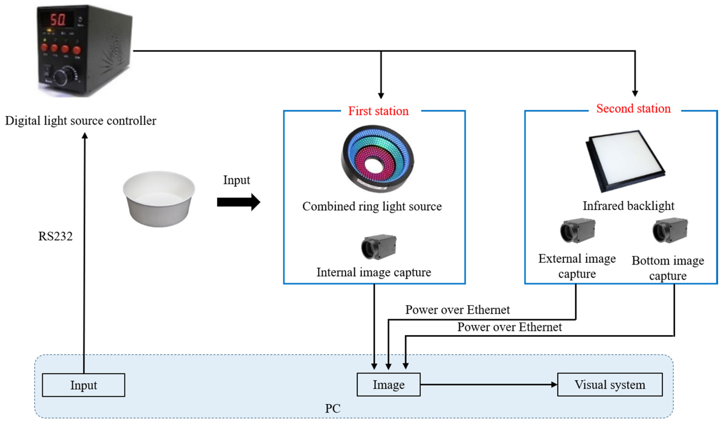
A machine vision system was used in this study, and the experimental setup is presented in Figure 2. The setup consisted of two inspection stations: the first station was used for internal image inspection using a combined ring light source, while the second station was used for external and bottom image inspections using an infrared backlight. The function of the first checkpoint was designed to inspect flaws inside the device under test, while the function of the second checkpoint was designed to inspect blemishes outside the device under test. The optical equipment system is investigated and focused on machine vision as its core. The system utilizes the RS232 communication interface to connect the optical equipment system to the computer, specifically through the light source controller. The computer specifications included an i7-6700 CPU and 8 GB of DDR4 RAM and the combined ring light source model used was CUBIC-AOI160-RGB. The CUBIC-3DPC24120-4S model was also used as the digital light controller, and the CUBIC-4FT150150-IR model as the infrared backlight. Regarding the analysis, process and methods were designed and investigated by ourselves to match our specific needs. Through this setup, the system is capable of adjusting the brightness of both the combined ring light source and the infrared backlight. The computer is powered using Power over Ethernet (PoE) and used to capture images from the camera, process the vision system images, and inspect the defects of the fabricated paper bowls. This paper utilized a 1/1.8” CMOS camera with the following specifications: an effective resolution of 1600 (H) × 1200 (V), a frame rate of 60 fps, pixel dimensions of 4.5 μm × 4.5 μm, and physical dimensions of 29 × 29 × 40 (mm).

2.2. Image Capture Methods

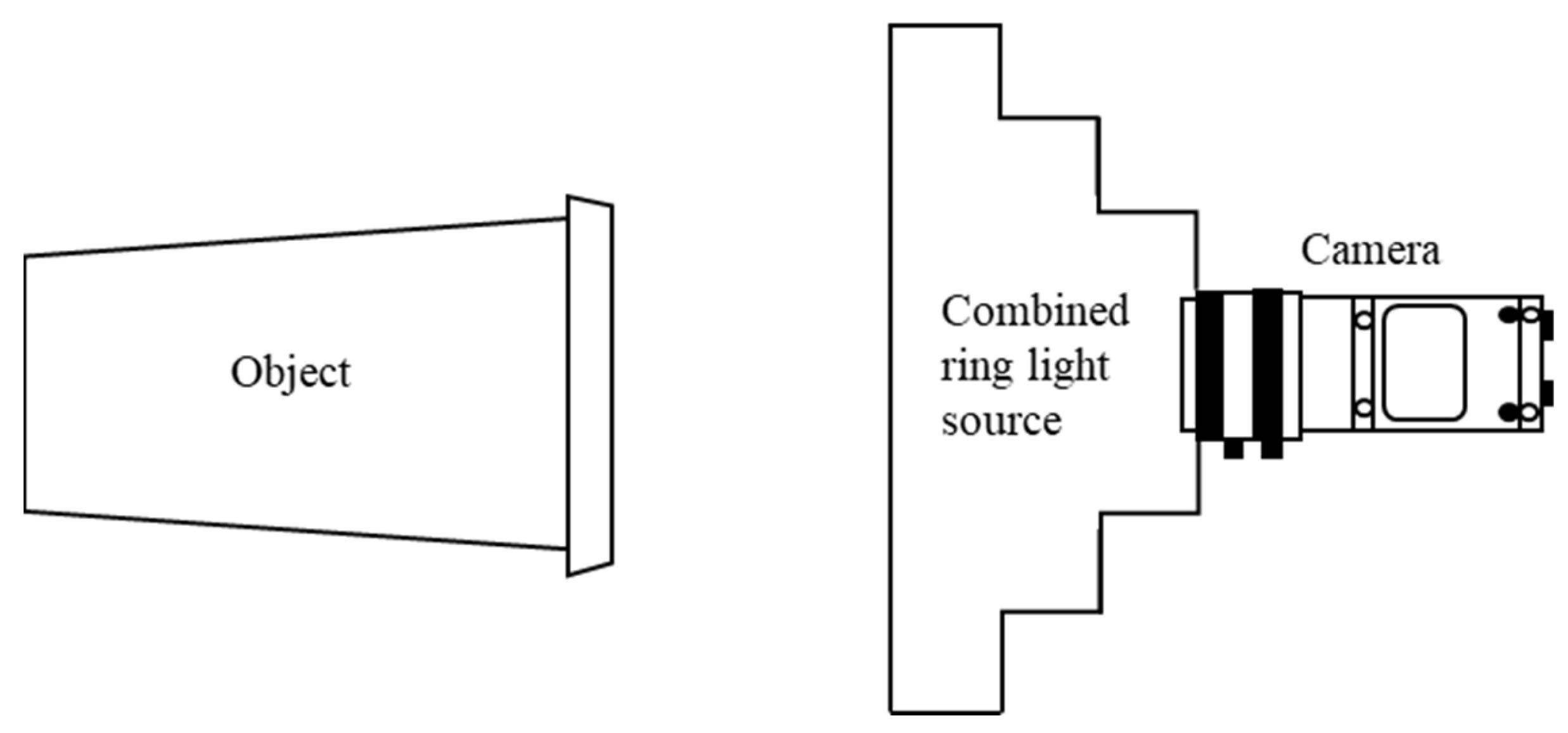
In this research project, disposable paper bowls were used as the objects of study and three different images, namely, the internal, external, and bottom images, were captured for further inspection. Figure 3 shows the environment setup for capturing the internal images, where the camera was used to capture the images of the inside of the inspected objects, and the captured images were saved for further analysis. The combined ring light source was used to assist the camera in capturing the internal images of the inspected objects. To capture the external images, four cameras were used, with each camera capturing one quarter of the exterior of the inspected objects. These four images were then combined and classified into a single category due to their similar exteriors. The environment configuration for capturing the external images is depicted in Figure 4, where an infrared backlight was placed under the inspected objects to act as an auxiliary light source. The capturing process for the bottom images was carried out in the same environment as that of the external images. The cameras took pictures of the paper bowls from around six different directions, enabling recognition of the images as 3D movements. Figure 5a–c show the images captured from the internal, external, and bottom of a paper bowl, respectively.

3. Image Processing Results and Discussion

3.1. Image Processing Method

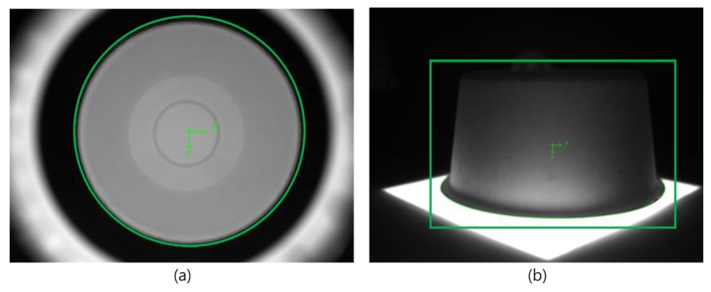
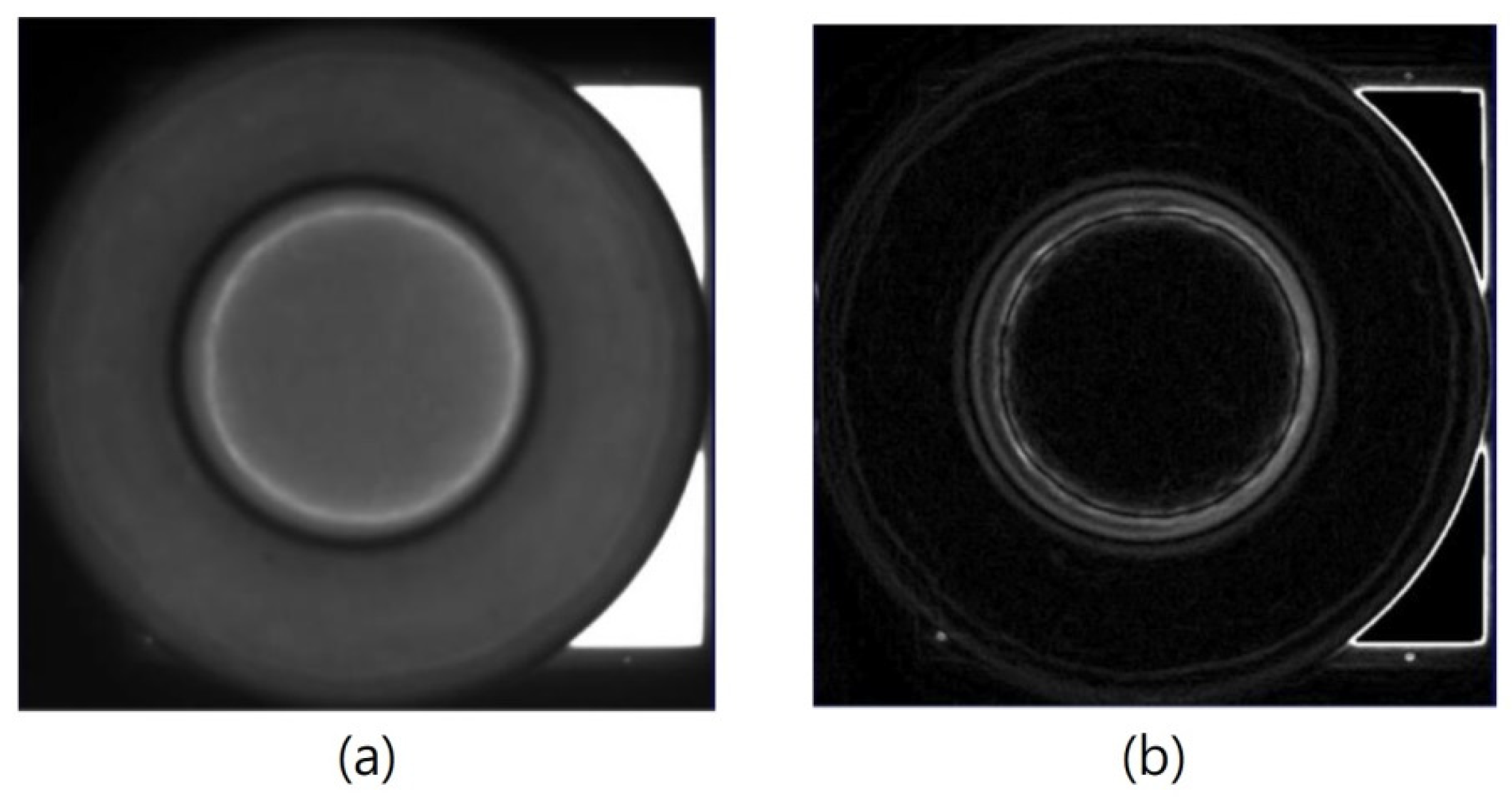
Template matching technology is a common approach to identify the search target in analyzed images [21,22]. In this technique, a template is an object in an image that is used for inspection. The paper bowl to be inspected had a diameter of 14 cm and a height of 8 cm, and the detected defects (dirt, burrs, holes, and thickness unevenness) being targeted for inspection should have a size larger than 0.2 cm. Figure 6a depicts an image with an inner template (region within the green circle) and Figure 6b shows an image with an outer template (region within the green box). The search target can be inspected in the image through matching it with the template, which has similar characteristics such as direction, curve, and line. The Sobel operator is used in two different algorithms, Magnitudeedge and Angleedge, with the former being more commonly used. Figure 7a,b compare the original image of a paper bowl with the image after being processed using Sobel’s Magnitudeedge algorithm. As shown in Figure 7, the edges of all objects become more distinct after the Sobel processing. When the inspected targets have an issue of uneven surface, Gaussian filtering is used to make the surface smoother and improve the uneven brightness problems.
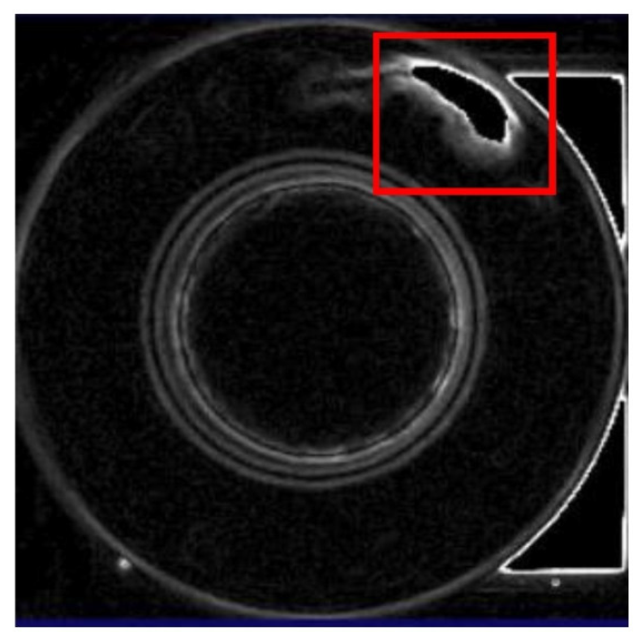
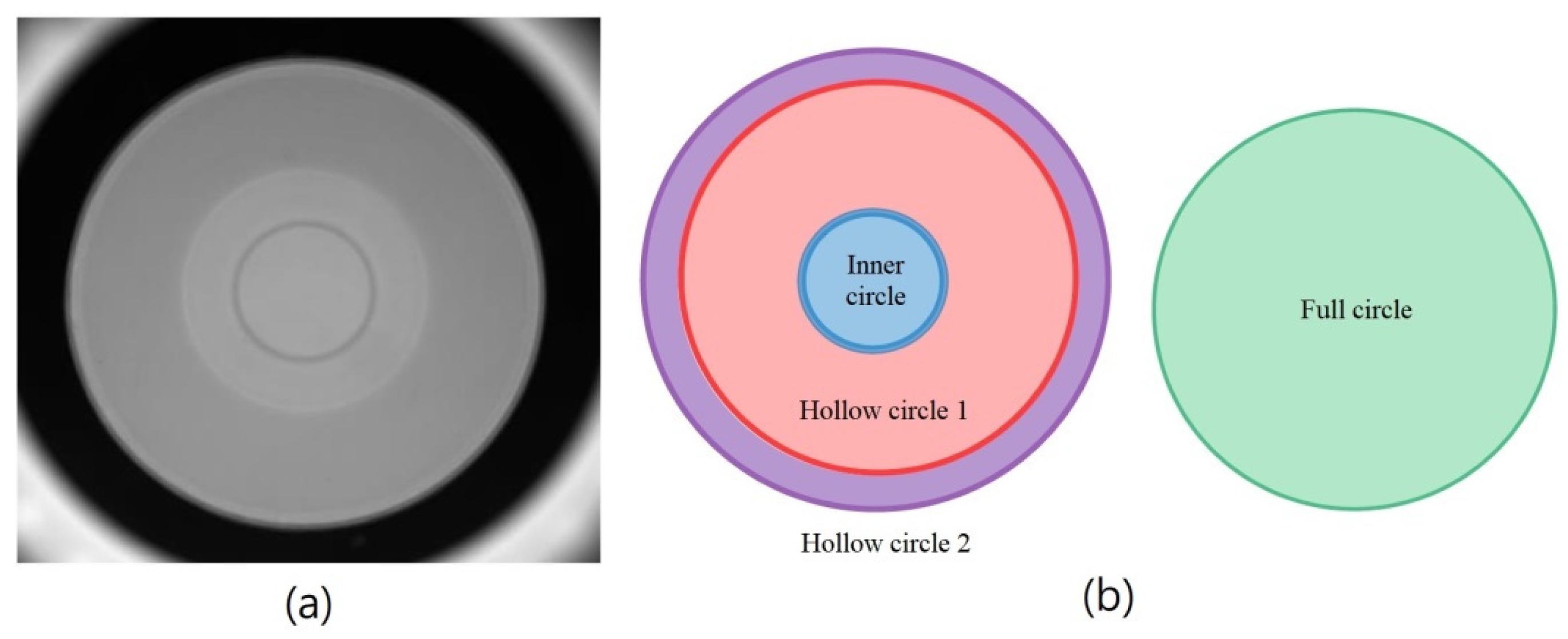
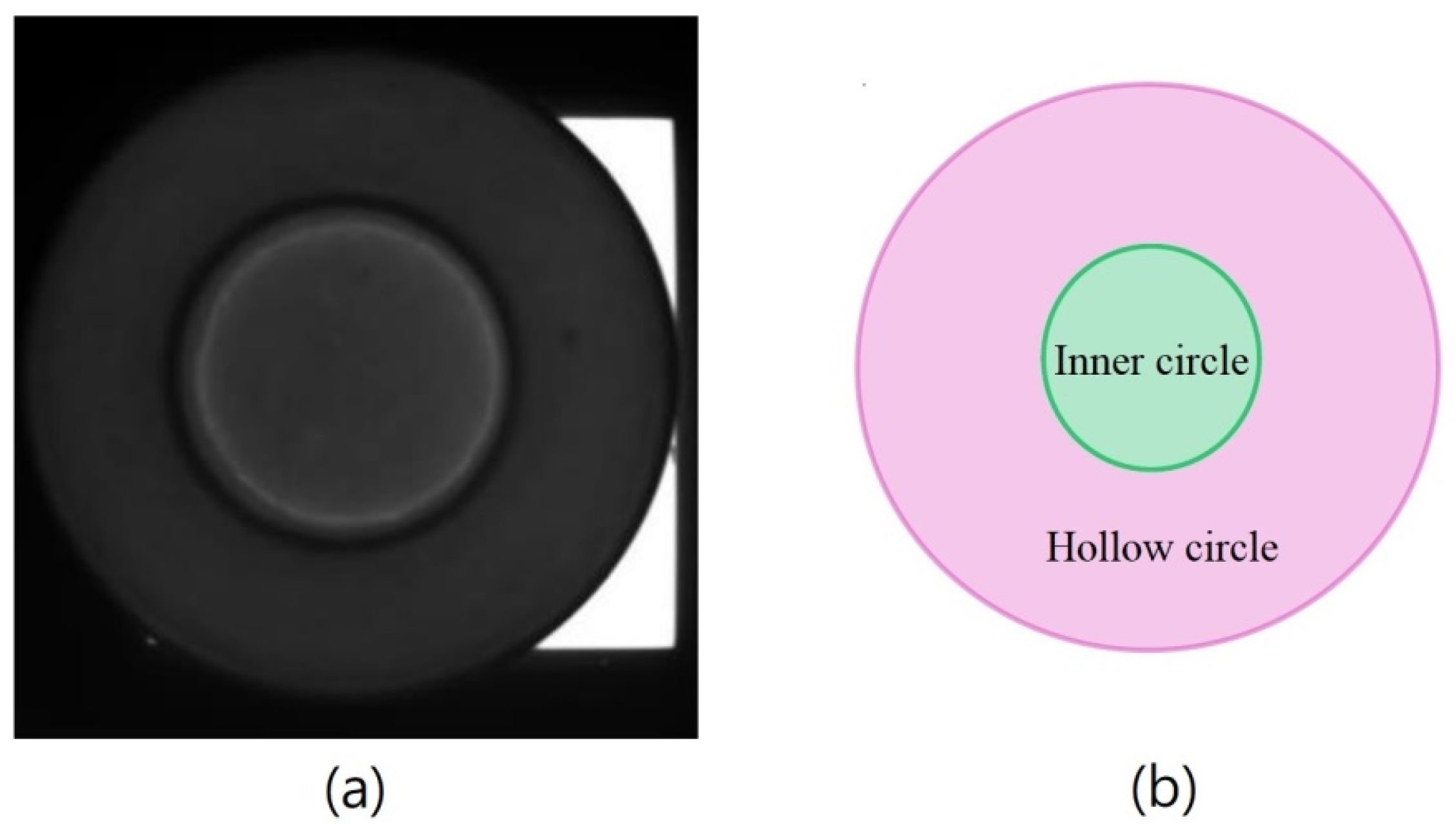
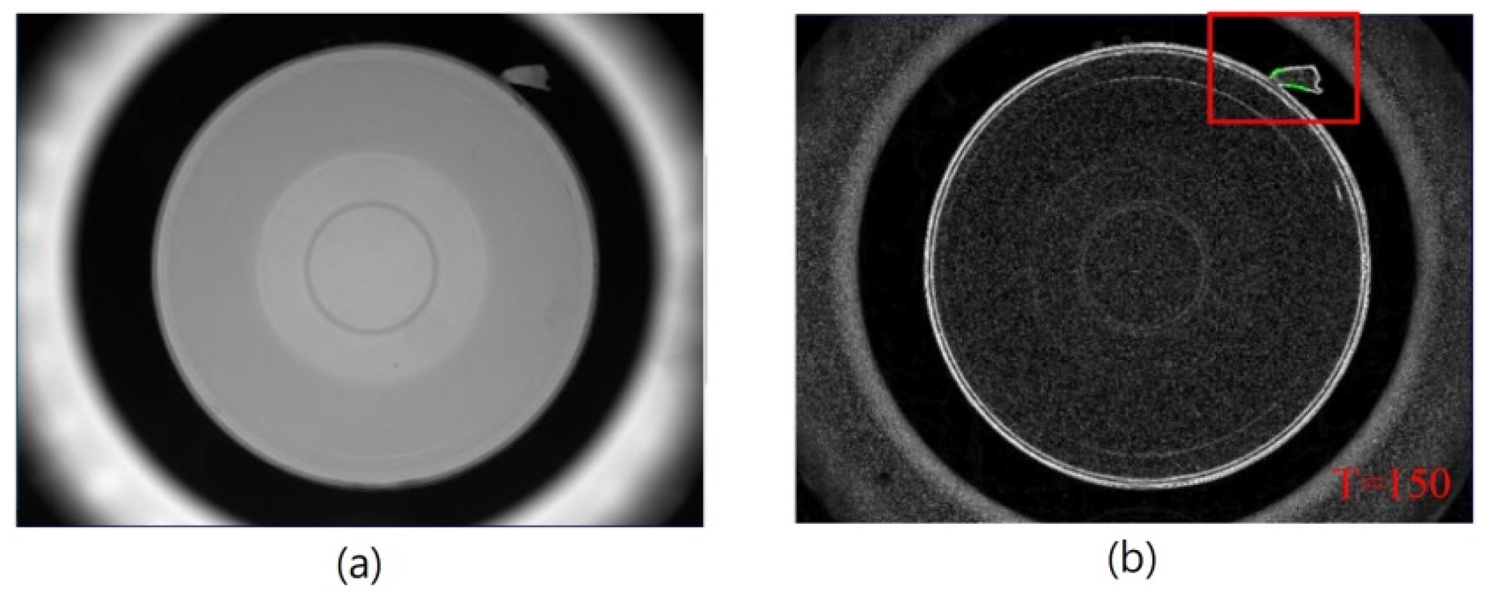
In this study, the investigated inspection system encountered two major problems. The first problem mainly concerns interior and bottom inspections. When the Sobel filter is applied to process the captured images, the edges of all processed objects become more apparent. As shown in Figure 8, after Sobel filtering, both the colors of the defect and edge contour in the red box turn white. To prevent misjudgments on defects, the edge contour must be separated from the defect. The second issue is caused by the perspective of external inspection. When the surfaces of the tested objects are closer to the infrared backlight, the bottom surfaces become brighter, which can cause uneven brightness. However, this problem can be improved through using segmentation and Gaussian filtering to process the images. Figure 9 shows the segmentation of the internal image of a bowl into pieces, with the inner circle and hollow circle 1 used to inspect dirt, hollow circle 2 used to inspect burrs, and the full circle used to inspect holes, as shown in Figure 10 and Figure 11. The main purpose of segmentation of the external and bottom images is to inspect for uneven thickness.
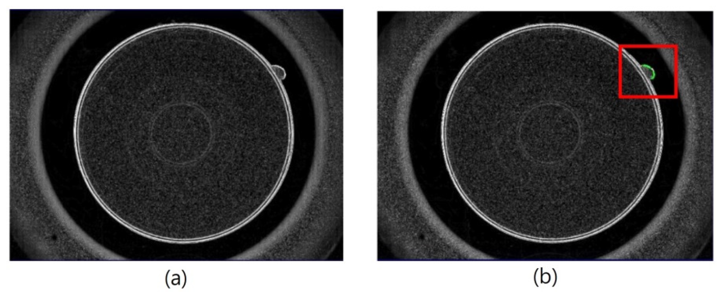
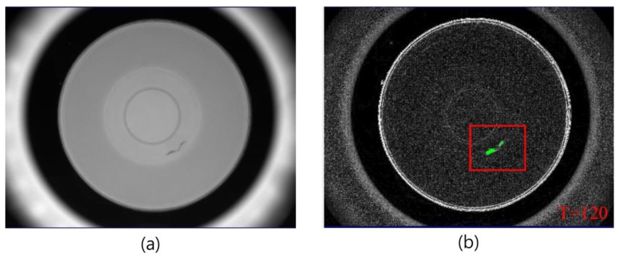
In order to distinguish between defects and background in the captured images, the binarization process was used to enhance the defect areas for further inspection. As the inspection pictures were obtained from a factory’s large-scale mechanized mass production line, and the environment was uniform and simple, 50 image samples were used as a benchmark, and the threshold was set via manual adjustment to achieve a balance between yield and output. Figure 12a shows the original captured image, indicating the presence of dirt inside a paper bowl. Figure 12b shows that when the binarization process was applied to the captured image, the region containing dirt was enhanced and made more visible. Figure 13a shows the presence of a burr inside a paper bowl, and Figure 13b demonstrates that the binarization process successfully enhanced the region containing the burr, even though it was small. These results demonstrate the effectiveness of the binarization process in enhancing the areas of defects present in the paper bowls for further inspection.

3.2. Image Processing Procedure

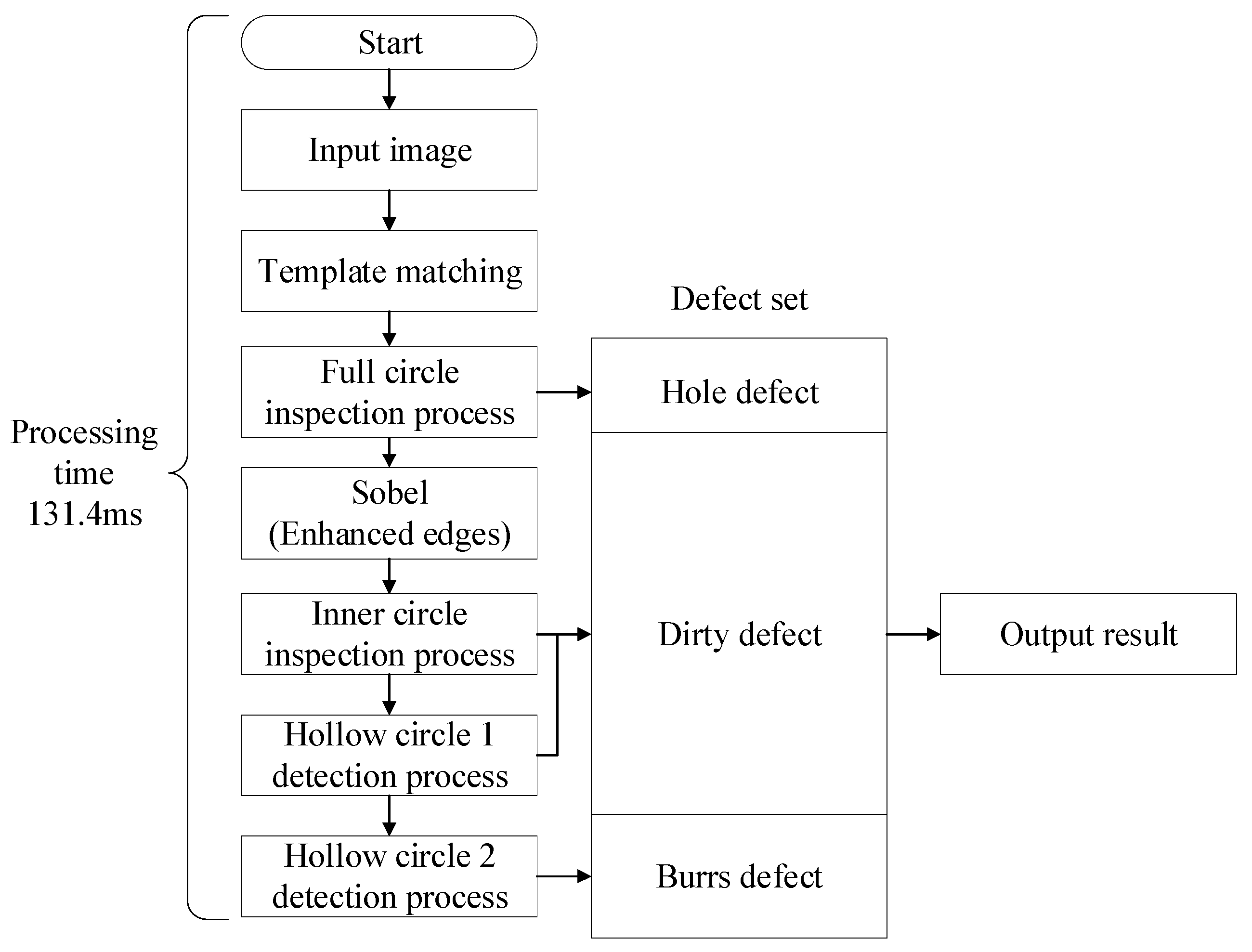
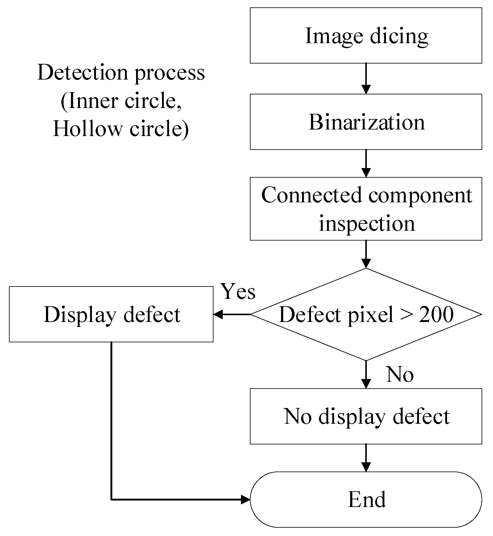
There are three inspection procedures for the paper bowls produced in the factory: internal, external, and bottom inspections. The internal inspection procedure, shown in Figure 14, involves matching the paper bowl image with a template to lock onto the target, followed by a full circle inspection process to inspect any holes or defects present in the paper bowls. The inspection process for internal paper bowl defects consists of three steps. Firstly, the full circle inspection process is used to inspect any holes present. Next, the Sobel operator is applied to enhance the edges of defects visible in the captured images. Finally, different circles are employed to inspect different types of defects. The inner circle and hollow circle 1 are used to identify dirty defects, while hollow circle 2 is used to inspect burr defects. In the full circle inspection process shown in Figure 14, the inner circle range is segmented out through an image segmentation process, and then a binarization process is performed. When the gray value is lower than a critical value assigned, this area will appear black, indicating the presence of a hole. The region for the hole is inspected and effectively enhanced. When the gray value exceeds the assigned critical value, it is displayed as white, representing the background. Therefore, the holes (defects) in the binarization process image have a distinct grayscale compared to the background. Subsequently, the connected component process is applied to further process the image via dividing adjacent pixels into the same block.
In the final step, if the calculated number of defective pixels is greater than 200, a defect is determined to be present. During the inspection process of the inner circle, hollow circle 1, and hollow circle 2, the image is segmented and binarized. Areas with gray values lower than those in the inner circle, hollow circle 1, or hollow circle 2 are recognized as background and displayed as black.
When the gray value of an area exceeds the assigned values in the inner circle, hollow circle 1, or hollow circle 2, it is identified as dirt, burrs, or uneven thickness, and displayed as white. The connected component process is then used to group adjacent pixels into the same block. Defects are identified when the number of inspected pixels exceeds 200. The average processing time for the internal inspection process of paper bowls was 131.4 ms, which will be presented later.
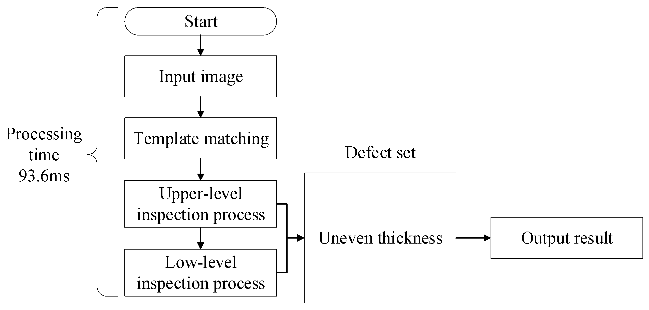
The flowchart for the external inspection process of a paper bowl is presented in Figure 15. Initially, the captured image is matched with the template to locate the target paper bowl. Subsequently, the upper layer inspection process is carried out to inspect for uneven thickness defects, followed by the bottom layer inspection process to inspect any such defects. Figure 16 shows the flowchart for the bottom inspection process. The first step of the upper layer inspection process is to apply a Gaussian filter to the image segmentation range to diffuse the bright uneven surface and achieve evenness. Next, the Sobel operator is used to enhance the contours of defects in the upper-level image. Finally, the binarization process is carried out, and areas with gray values below a critical threshold are identified as black and recognized as background.
On the other hand, the area with a gray value higher than a critical value is recognized as white, which indicates uneven thickness. The connected component process is then used to group adjacent pixels into the same block, and the defect is displayed when the pixels are judged to be greater than 200. The average processing time of the external inspection process of the paper bowl was 124.6 ms, which will be presented later. When the gray value falls below the critical value, the pixel is displayed as black, indicating the background. Conversely, when the gray value exceeds the critical value, it is displayed as white, indicating uneven thickness. The connected component process is then applied to group adjacent pixels into the same block. If the number of pixels exceeds 200, the result is classified as a defect. The external inspection process of a paper bowl took an average processing time of 93.6 ms.
The flowchart for the bottom inspection process of a paper bowl is presented in Figure 17. The captured image is first matched with the template to identify the defective areas of the paper bowl. Subsequently, Sobel processing is applied to enhance the visibility of the defects. The inspection process then proceeds with the adoption of inner and hollow circle inspection methods to inspect uneven thicknesses at different positions. The inspection procedures for the inner and hollow circles at the bottom of a paper bowl are illustrated in Figure 18. The captured image is first segmented into blocks and then binarized. Areas with gray values lower than those of the inner and hollow circles are identified as background and shown as black. Conversely, areas with gray values higher than those of the inner and hollow circles are identified as uneven thickness and shown as white. The connected component process is then used to group adjacent pixels into the same block. If a block is judged to have more than 200 defect pixels, a defect result is displayed. The bottom inspection process of a paper bowl takes 94.4 ms.

3.3. Defect Inspection Results

As each bowl has unique defects, the processing time for each corresponding image varies. To determine the average processing time, 20 samples were taken for each of the internal, external, and bottom inspection processes, and the results are shown in Table 1. However, this study had performed calculations using a larger sample size; due to space limitations in the paper, not all data were able to be included in the results. It is worth noting that the statistical outcomes are comparable to those obtained in 20 previous iterations. The inspection time for internal defects ranged from 127 to 136 ms, with an average of 131.4 ms. This demonstrates that the system investigated effectively inspects internal defects in the fabricated paper bowls, with an error margin of less than 5 ms. The inspection time for external defects ranged from 89 to 98 ms, with an average inspection time of 93.6 ms and an error margin of less than 5 ms. Similarly, the inspection time for bottom defects ranged from 90 to 100 ms, with an average of 94.4 ms and a maximum error margin of 5 ms. The system achieved a 100% inspection accuracy rate for captured images to inspect defects in the internal, external, and bottom areas of the produced paper bowls. The investigated AOI system effectively inspects various types of defects in the paper bowls. The average measurement and processing time for inspecting these defects was 319.4 ms. The results demonstrate that the Gaussian filter, Sobel operator, binarization, and connected component processes effectively enhance the recognition of captured images using the self-assembled inspection system.
To demonstrate the effectiveness of the investigated optical automatic inspection system, images captured at different positions and inspection images with various defects are compared and presented. The system comprises an industrial camera, ring light sources, infrared backlights, a computer, and machine vision software that includes Gaussian filtering, Sobel operator, binarization, and either 4-connecting or 8-connecting component processes. Figure 19a displays the original image of a paper bowl, where a small internal burr is visible. Figure 19b presents the processed internal image that effectively inspected the burrs in the paper bowl, thereby demonstrating the effectiveness of the investigated technology in inspecting internal burrs. Similarly, Figure 20a illustrates the original image of a paper bowl that contains internal dirt, while Figure 20b displays the corresponding inspected image that accurately inspected the dirt within the bowl. Figure 21a displays an image of a paper bowl with a small internal hole, while Figure 21b shows the corresponding processed image that accurately inspected the edge and defined the region of the hole. Figure 22a,b present the original and processed images of a paper bowl with uneven thickness at the external upper layer, and in Figure 22a, the light transmittance test is conducted on the paper bowl to identify any variations in thickness across its surface. Meanwhile, Figure 23a,b display the original and processed images of a paper bowl with uneven thickness at the bottom. Both figures illustrate the inspection and definition of uneven thickness in different positions of the paper bowl.
The images presented in this research depict the actual mass-produced products inspected using the investigated technology. To classify the defects, the inspection results are compared with the corresponding images of the actual products; however, distinguishing the relevant content visually can be challenging. Figure 19 illustrates a burr defect, Figure 20 shows a dirt defect, and Figure 21 depicts a hole defect. Visually, the main differences between these images are differences in color shades. In previous research, Park et al. employed deep learning to inspect defects in paper products but only achieved an inspection rate of 96.5% [23]. Bing’s research utilized machine vision technology to inspect defects in paper products and achieved inspection rates ranging from 96% to 100% [24]. The inspection images presented in Figure 19, Figure 20, Figure 21, Figure 22 and Figure 23 demonstrate the effectiveness of the investigated system in inspecting defects at various positions in the manufactured paper bowls. Subsequently, the average time consumed by the machine vision system for detecting paper–plastic products is 0.3 s. The system has been tested for inspecting thousands of paper bowls on the production line, achieving an impressive inspection accuracy of 99.66%. This study utilizes traditional image recognition methods, and the research findings demonstrate that the system developed in this study can achieve faster processing and requires less code when dealing with simple recognition problems. In comparison to deep learning methods that require a large amount of training data, the results of training sometimes overfit and do not meet expectations. When faced with simple color threshold differentiations, the system developed in this project utilizes traditional image recognition, which achieves higher accuracy and greater efficiency, meeting the expected outcomes. These results validate the practicality of the investigated AOI system for inspecting defects in paper products.

4. Conclusions

In this study, an automatic optical inspection system (AOI) was successfully self-assembled and combined with different image processing software to inspect defects in fabricated paper bowls. For the manufactured bowls, the average inspection time for internal defects was 131.4 ms, while for external and bottom defects, the average inspection times were 93.6 ms and 94.4 ms, respectively. The accuracy rates for inspecting defects in the internal, external, and bottom areas of the produced paper bowls using captured images were 100%. Additionally, a high inspection accuracy rate of 99.66% was achieved for the paper bowls manufactured on the production line. In conclusion, the combination of a self-assembling AOI system with various image processing software can effectively increase defect inspection efficiencies in manufactured paper products and resolve the issue of visual fatigue associated with manual inspections. The investigated experimental system involved a collaboration with the manufacturer of the paper bowl manufacturing machine. Several tests were conducted within the premises of the paper bowl manufacturing factory itself, making it a practical and applicable approach for future implementation in the industry.

Author Contributions

Conceptualization, S.Y., Y.-H.L., C.-W.C., P.G., Z.X., S.C. and C.-F.Y.; methodology, S.Y., Y.-H.L. and C.-F.Y.; software, S.Y., Y.-H.L., C.-W.C., P.G., Z.X., S.C. and C.-F.Y.; validation, S.Y., Y.-H.L., C.-W.C., P.G. and C.-F.Y.; formal analysis, S.Y., Y.-H.L., C.-W.C., P.G., Z.X. and C.-F.Y.; investigation, S.Y., Y.-H.L. and C.-F.Y.; data curation, S.Y., Y.-H.L., C.-W.C., P.G., Z.X., S.C. and C.-F.Y.; writing—original draft preparation, S.Y., Y.-H.L. and C.-F.Y.; writing—review and editing, S.Y., Y.-H.L. and C.-F.Y.; visualization, S.Y., Y.-H.L., C.-W.C., P.G., Z.X., S.C. and C.-F.Y. All authors have read and agreed to the published version of the manuscript.

Funding

This work was supported by the Natural Science Foundation Project of Fujian Provincial Department of Science and Technology (No. 2023J01976), project of Doctor Support Plan of Longyan University (No. LB2018031), Fujian Science and Technology Program (No. 2021Y0074), Fujian Science and Technology Innovation Fund (No. 2020SHQM14; XLQM009), Education and Research Project for Young and Middle aged Teachers of Fujian Provincial Department of Education(No. JAT200455), and the MOST 110-2221-E-032-018-MY2.

Institutional Review Board Statement

Not applicable.

Informed Consent Statement

Not applicable.

Data Availability Statement

Not applicable.

Conflicts of Interest

The authors declare no conflict of interest.

References

  1. A Environmental Protection Agency. Plastic-Reduction Business Boom Worldwide: Chung Hwa Pulp Launch Non-Plastic Pulp-Based Full Product Line. Available online: https://topic.epa.gov.tw/edcs/cp-362-8978-30510-6.html (accessed on 25 December 2020). (In Chinese)
  2. Babica, M.; Farahania, M.A.; Wuesta, T. Image Based Quality Inspection in Smart Manufacturing Systems: A Literature Review. Prodedia CIRP 2021, 103, 262–267. [Google Scholar] [CrossRef]
  3. Prinsloo, J.; Sinha, S.; Solms, B.V. A Review of Industry 4.0 Manufacturing Process Security Risks. Appl. Sci. 2019, 9, 5105. [Google Scholar] [CrossRef]
  4. Taha, E.M.; Emary, E.; Moustafa, K. Automatic Optical Inspection for PCB Manufacturing: A Survey. Int. J. Sci. Eng. Res. 2014, 5, 1095–1102. [Google Scholar]
  5. Abu Ebayyeh, A.A.R.M.; Mousavi, A. A Review and Analysis of Automatic Optical Inspection and Quality Monitoring Methods in Electronics Industry. IEEE Access 2020, 8, 183192–183271. [Google Scholar] [CrossRef]
  6. Choi, J.; Kim, B.; Jeon, J.Y.; Lee, H.J.; Lim, E.; Rhee, C.E. A Lightweight and Efficient GPU for NDP Utilizing Data Access Pattern of Image Processing. IEEE Trans. Comput. 2022, 71, 13–26. [Google Scholar] [CrossRef]
  7. Mendoza, Q.A.; Pordesimo, L.; Neilsen, M.; Armstrong, P.; Campbell, J.; Mendoza, P.T. Application of Machine Learning for Insect Monitoring in Grain Facilities. AI 2023, 4, 348–360. [Google Scholar] [CrossRef]
  8. Moraru, L.; Obreja, C.D.D.; Dey, N.; Ashour, A.S. Chapter 9–Dempster-Shafer Fusion for Effective Retinal Vessels’ Diameter Measurement. In Soft Computing Based Medical Image Analysis; Academic Press: Cambridge, MA, USA, 2018; pp. 149–160. [Google Scholar]
  9. Cabello, F.; León, J.; Iano, Y.; Arthur, R. Implementation of a fixed-point 2D Gaussian Filter for Image Processing based on FPGA. In Proceedings of the 2015 Signal Processing: Algorithms, Architectures, Arrangements, and Applications (SPA), Poznan, Poland, 23–25 September 2015; pp. 28–33. [Google Scholar]
  10. Vijayarani, S.; Vinupriya, M. Performance Analysis of Canny and Sobel Edge Detection Algorithms in Image Mining. Int. J. Innov. Res. Comput. Commun. Eng. 2013, 1, 1760–1767. [Google Scholar]
  11. Uss, M.; Vozel, B.; Lukin, V.; Chehdi, K. Exhaustive Search of Correspondences between Multimodal Remote Sensing Images Using Convolutional Neural Network. Sensors 2022, 22, 1231. [Google Scholar] [CrossRef] [PubMed]
  12. Mustafa, W.A.; Abdul Kader, M.M.M. Binarization of Document Images: A Comprehensive Review. J. Phys. Conf. Ser. 2018, 1019, 12023. [Google Scholar] [CrossRef]
  13. Mehta, N.; Braun, P.X.; Gendelman, I.; Alibhai, A.Y.; Arya, M.; Duker, J.S.; Waheed, N.K. Repeatability of binarization thresholding methods for optical coherence tomography angiography image quantification. Sci. Rep. 2020, 10, 15368. [Google Scholar] [CrossRef] [PubMed]
  14. Esquembri, S.; Nieto, J.; Carpeño, A.; Ruiz, M.; Astrain, M.; Costa, V.; Gracia, A. Application of Heterogeneous Computing Techniques for the Development of an Image-Based Hot Spot Detection System Using MTCA. IEEE Trans. Nucl. Sci. 2021, 68, 2151–2158. [Google Scholar] [CrossRef]
  15. Kim, S.; Yoo, J.; Choi, H.; Seo, J.; Lee, S.; Won, S.M.; Park, J.H.; Heo, K. In-Depth Study of 3D Color-Resist Coating Process for Optically Uniform Image Sensors. IEEE Access 2021, 9, 146525–146532. [Google Scholar] [CrossRef]
  16. Callens, N.; Gielen, G.G.E. Analysis and Comparison of Readout Architectures and Analog-to-Digital Converters for 3D-Stacked CMOS Image Sensors. IEEE Trans. Circuits Syst. I Regul. Pap. 2021, 68, 3117–3130. [Google Scholar] [CrossRef]
  17. Wu, Y.; Wen, J.; Zhang, P. Application of AOI light source modes in multi-chip modules inspection. In Proceedings of the 19th International Conference on Electronic Packaging Technology (ICEPT), Shanghai, China, 8–11 August 2018; pp. 141–143. [Google Scholar]
  18. Peng, D.; Zhang, K.; Liu, Z. Design and Fabrication of Fine-Pitch Pixelated-Addressed Micro-LED Arrays on Printed Circuit Board for Display and Communication Applications. IEEE J. Electron Devices Soc. 2017, 5, 90–94. [Google Scholar] [CrossRef]
  19. Sim, K.; Yang, J.; Lu, W.; Gao, X. Blind Stereoscopic Image Quality Evaluator Based on Binocular Semantic and Quality Channels. IEEE Trans. Multimed. 2022, 24, 1389–1398. [Google Scholar] [CrossRef]
  20. Yang, J.; Zhao, Y.; Jiang, B.; Lu, W.; Gao, X. No-Reference Quality Evaluation of Stereoscopic Video Based on Spatio-Temporal Texture. IEEE Trans. Multimed. 2020, 22, 2635–2644. [Google Scholar] [CrossRef]
  21. Cheng, J.; Wu, Y.; AbdAlmageed, W.; Natarajan, P. QATM: Quality-Aware Template Matching for Deep Learning. In Proceedings of the 2019 IEEE/CVF Conference on Computer Vision and Pattern Recognition (CVPR), Long Beach, CA, USA, 15–20 June 2019; pp. 11545–11554. [Google Scholar]
  22. Roh, D.W.; Jeon, J.W. Hardware Architecture Design for Template Matching. In Proceedings of the 2019 International SoC Design Conference (ISOCC), Jeju, Republic of Korea, 6–9 October 2019; pp. 287–288. [Google Scholar]
  23. Park, C.H.; Kwon, Y.H.; Lee, S.O.; Jung, J.Y. Automated Inspection for Paper Cups Using Deep Learning. J. Korean Soc. Precis. Eng. 2017, 34, 449–453. [Google Scholar] [CrossRef]
  24. Bing, Z.L. Inspection of the outer packaging quality of paper cups based on machine vision. Comput. CD Softw. Appl. 2012, 10, 56–58. (In Chinese) [Google Scholar]
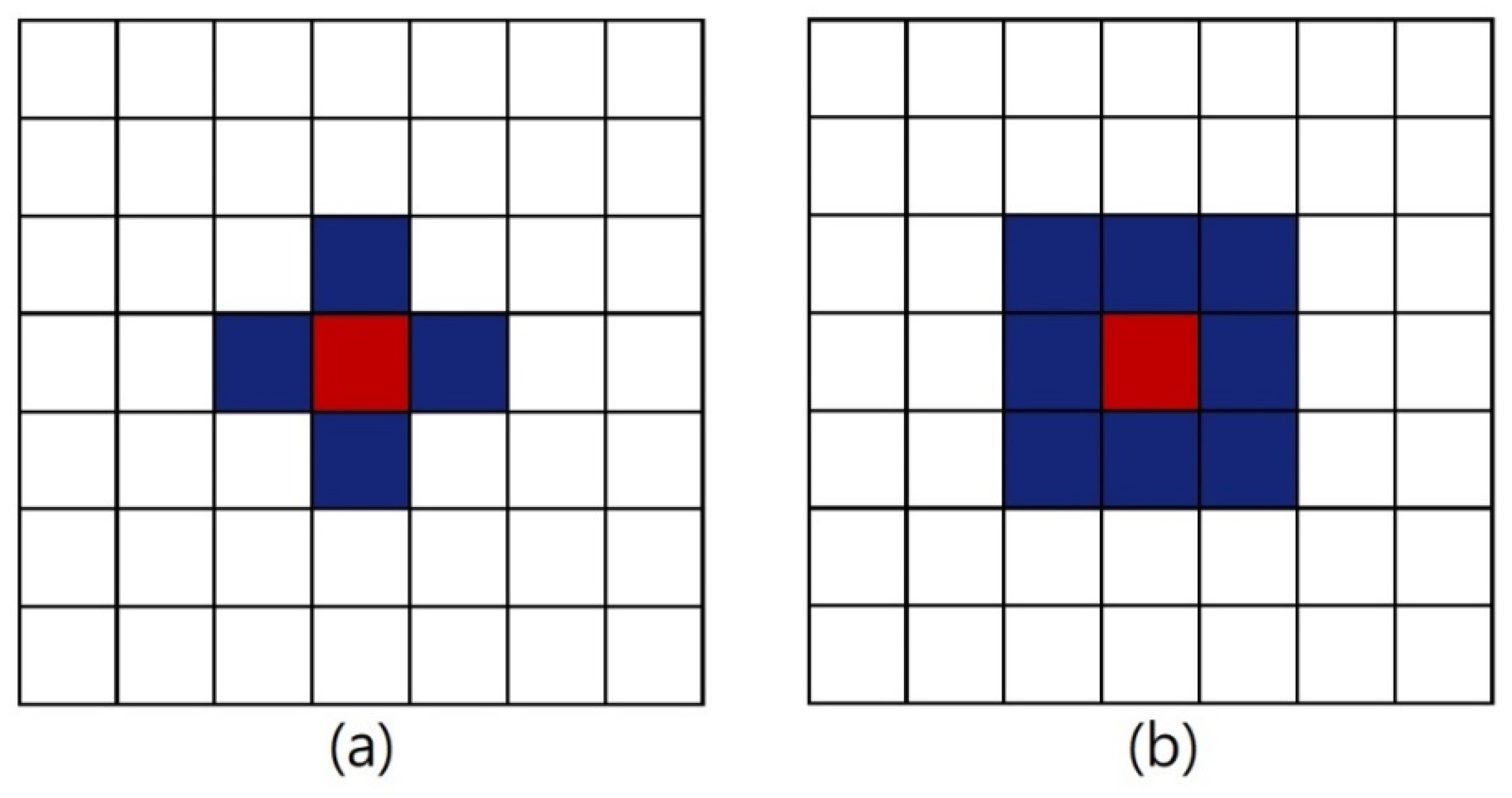
Figure 1. (a) Four-connected component and (b) eight-connected component.
Photonics 10 00686 g001
Figure 2. Architecture diagram of the investigated system.
Photonics 10 00686 g002
Figure 3. Environment configuration for capturing the internal images.
Photonics 10 00686 g003
Figure 4. Environment configuration for capturing the external images.
Photonics 10 00686 g004
Figure 5. (a) Internal capturing image, (b) external capturing image, and (c) bottom capturing image of a paper bowl.
Photonics 10 00686 g005
Figure 6. (a) Matching of the inner template and (b) matching of the outer template of a paper bowl.
Photonics 10 00686 g006
Figure 7. (a) Original image and (b) the Sobel’s Magnitudeedge processed result of a paper bowl.
Photonics 10 00686 g007
Figure 8. Image of the edge defect. Red square: the region to show the defect.
Photonics 10 00686 g008
Figure 9. (a) Original image and (b) schematic diagram for the interior segmentation of a bowl.
Photonics 10 00686 g009
Figure 10. (a) Original image and (b) schematic diagram for external segmentation of a bowl.
Photonics 10 00686 g010
Figure 11. (a) Original image and (b) schematic diagram for the bottom segmentation of a bowl.
Photonics 10 00686 g011
Figure 12. (a) Original image and (b) binarization processing image of dirt inside a paper bowl. Red square: the region to show the defect, green line: the dirt.
Photonics 10 00686 g012
Figure 13. (a) Original image and (b) binarization processing image of a burr inside a paper bowl. Red square: the region to show the defect, green line: a burr.
Photonics 10 00686 g013
Figure 14. Internal inspection process of a paper bowl.
Photonics 10 00686 g014
Figure 15. External inspection process of a paper bowl.
Photonics 10 00686 g015
Figure 16. Inspection processes of the outer, upper, and bottom parts of a paper bowl.
Photonics 10 00686 g016
Figure 17. Inspection process of the bottom part of a paper bowl.
Photonics 10 00686 g017
Figure 18. Inspection processes for the bottom parts of the inner circle and hollow circle of a paper bowl.
Photonics 10 00686 g018
Figure 19. (a) Original image and (b) the processing image of internal burr in a paper bowl. Red square: the region to show the defect, green line: a burr.
Photonics 10 00686 g019
Figure 20. (a) Original image and (b) the processing image of internal dirt in a paper bowl. Red square: the region to show the defect, green line: a dirt.
Photonics 10 00686 g020
Figure 21. (a) Original image and (b) the processing image of internal hole in a paper bowl. Red square: the region to show the defect, green line: a hole.
Photonics 10 00686 g021
Figure 22. (a) Original image and (b) the processing image for uneven thickness located at the external upper layer of a paper bowl. Red square: the region to show the defect, green line: region for uneven thickness.
Photonics 10 00686 g022
Figure 23. (a) Original image and (b) the inspection image for uneven thickness located at the bottom of a paper bowl. Red square: the region to show the defect, green line: region for uneven thickness.
Photonics 10 00686 g023
Table 1. Results of operation time of defect inspection for a paper bowl.
SampleInternal (ms)External (ms)Bottom (ms)
11349294
21319493
31338999
41359695
51319297
61359695
71299093
81279895
91329395
101299791
111319093
121349693
1313291100
141319694
151329193
161279890
171299195
181369691
191329094
201289598
Average131.493.694.4
Total319.4
Disclaimer/Publisher’s Note: The statements, opinions and data contained in all publications are solely those of the individual author(s) and contributor(s) and not of MDPI and/or the editor(s). MDPI and/or the editor(s) disclaim responsibility for any injury to people or property resulting from any ideas, methods, instructions or products referred to in the content.