2.1. Analysis of Eye Hole Units Design
The novel eye hole method is to make eye hole units on the substrate. Then, the substrate with the eye hole units is fixed in front of IRFPAs to achieve the crosstalk of the small element IRFPAs test. The design, preparation, and application of eye hole units are analyzed.
(1) Design and analysis of a single eye hole unit
The easiest way to realize the crosstalk detection for small element IRFPAs is to test the crosstalk of the single detection photosensitive element with a single eye hole unit. This scheme is easy to implement, and there is no need to consider the crosstalk of the surrounding detection photosensitive elements. The single eye hole unit is to make an eye hole on the substrate. The transmittance of the eye hole in the substrate is 100%, while the transmittance of the other component in the substrate is 0.
But the disadvantage of this method is that it can only test the crosstalk of a single detection photosensitive element each time. In order to obtain the crosstalk of multiple detection photosensitive elements, it is necessary to make multiple substrates of the single eye hole unit and conduct multiple alignment tests. The contrastability of the test data decreases with multiple clamping treatments of the IRFPAs. The method not only cannot guarantee the accuracy of the test data, but also needs to make multiple substrates of the single eye hole unit with different locations, so as to test multiple crosstalk data for analysis and processing and to exclude the effects of abnormal data.
The optimized crosstalk detection method for small element IRFPAs is to closely arrange the graphics of the single eye hole unit or arrange it as needed. This method is also easy to implement. It is conducive to subsequent data processing analysis, and accurate crosstalk test results can be obtained because the crosstalk of each eye hole unit is obtained under the same test condition. However, this method needs to consider the number of detection photosensitive elements contained in the graphic of the eye hole unit. It needs to be designed to eliminate the string of the measured eye hole to the adjacent eye hole to ensure the accuracy and effectiveness of the crosstalk. Therefore, the crosstalk of a single eye hole unit test is analyzed. The smallest eye hole unit is determined according to the test results.
The central opening has full transmittance (the transmittance is close to 100%) and the surrounding full cutoff (the transmittance is 0). Under normal circumstances, the response voltage of the single eye hole is normal when it is fully penetrated at the central opening, and 0 when it is fully cut off at the surrounding area. It not only avoids interference from other eye holes, but also allows for clear and accurate test results. In
Figure 1, the black represents the full cutoff, and the white represents the full transmission.
(2) Design and analysis of eye hole units for experiments
The eye hole units for experiments can be tightly arranged or arranged according to the need. The crosstalk of the eye hole unit graphic obtained by the novel eye hole method is obtained under the same test condition. It can not only solve the need to make multiple substrates with the single eye hole unit to align the test to obtain multiple crosstalk data, but also acquire multiple crosstalk test results at the same time, increasing the accuracy and comparability of the data.
There are two options for the eye hole unit. One is to select 9 detection elements in the box as the eye hole unit, as shown in
Figure 1. The other is to select 25 detection elements in the box as the eye hole unit, as shown in
Figure 2. Regardless of which method is selected, it is necessary to ensure that the crosstalk between the adjacent eye hole units and the tested eye hole unit is close to zero. It is conducive to obtaining the experimental data of 9 detection elements and 25 detection elements as the eye hole unit at the same time, and then obtaining the optimal eye hole unit for a lithography pattern through results analysis.
2.2. Eye Hole Units Preparing
In the design scheme, the transmittance full cutoff can be achieved by adopting a black opaque coating, or by using the growth gold film blocking radiation. Considering the controllability of the eye hole size and the feasibility of the operation, and the subsequent eye hole units’ preparation, the latter’s preparation method is selected here. For the fully transparent eye hole, it is only necessary to consider choosing substrate materials with a high infrared transmittance rate, so that the transmittance of the eye hole is close to 100%. The preparation of substrates with eye hole units can be corroded or stripped. The preparation process includes the following: the selection and pre-processing of the substrate, the growth of gold film, and the preparation of eye hole units. Quartz glass is used as the substrate and cleaned using a standard method. In order to ensure the high pass rate of the quartz glass within the range of (3.7 μm~4.8 μm), the quartz glass is polished to less than 150 μm. The deadline of the quartz glass is extended to 4.8 μm. The gold film on the surface of the substrate is grown using ultra-vacuum magnetic sputtering equipment, with a thickness of 0.1 μm.
2.3. Method Application
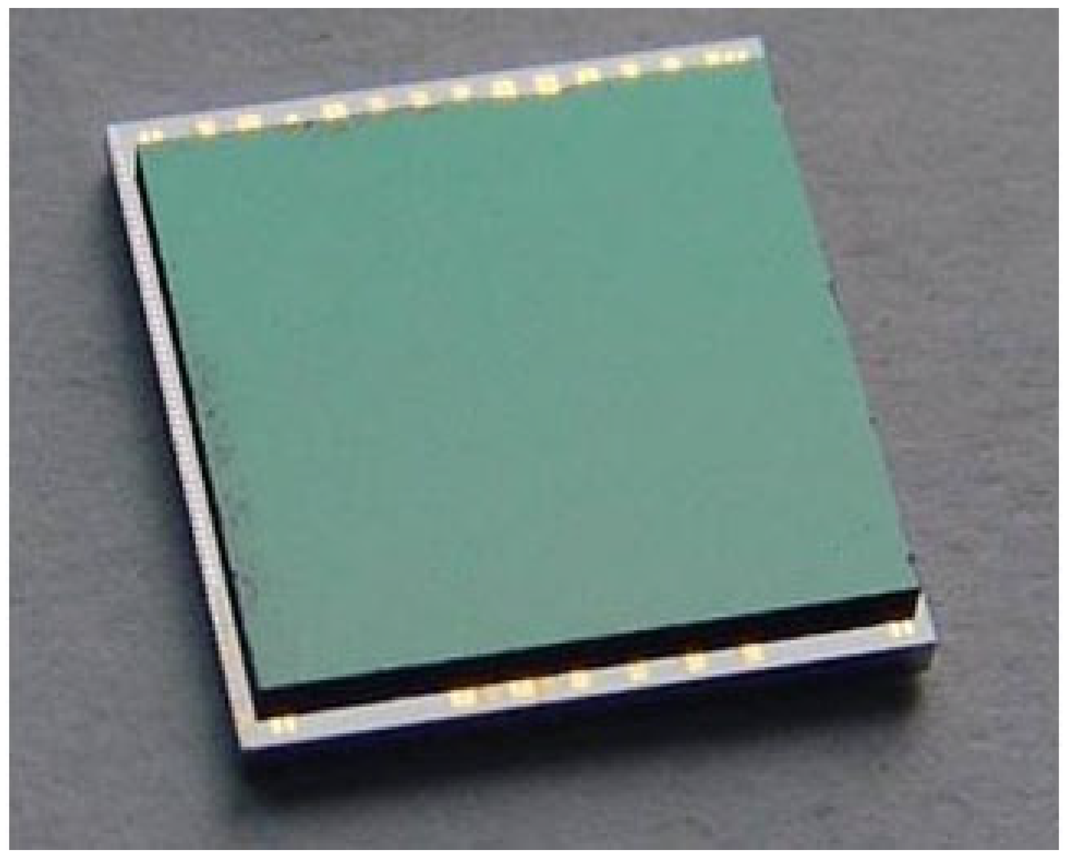
The experimental sample InSb arrays are first processed as follows: an n-type InSb substrate is used, a P-type layer is obtained through the diffusion Cd, and a surface with mesa is obtained by photolithography and etching. After the passivation of the mesa, a chrome gold layer is evaporated and then electrodes are obtained through photolithography and corrosion processes. The InSb arrays with 50 μm × 50 μm and 25 μm × 25 μm are designed and prepared. After the chips are prepared, the developed InSb arrays and the readout circuit arrays are photolithographed with indium column windows and evaporated with indium film at the same time. The indium column arrays are obtained through a stripping process, and then connected through flip-chip bonding. The flip-chip bonding devices are assembled and encapsulated after bottom filling, thinning polishing, and the vapor deposition of anti-reflection film. The InSb IRFPA is shown in
Figure 3.
The small light point method and the novel eye hole method are used to test the crosstalk of InSb IRFPA with the element size of 50 μm × 50 μm in the same coordinate point detection photosensitive element, respectively. Then, the novel eye hole method is used to test the crosstalk of InSb IRFPAs with the element size of 25 μm × 25 μm. According to the above methods, two substrates with eye hole units are designed and prepared.
The prepared substrates with eye hole units are installed in front of the IRFPAs. Each eye hole unit is aligned with each photosensitive element of the IRFPAs. The schematic diagram of the alignment structure is shown in
Figure 4. The IRFPAs with the eye hole unit are subsequently tested by the IRFPAs test system. The obtained test data of the response voltage are converted into the test data of the crosstalk, and the crosstalk of small element IRFPAs is analyzed.


