Article

PTFE-Based Circular Terahertz Dielectric Waveguides

1
University of Chinese Academy of Sciences, Beijing 100049, China
2
The CAS Key Laboratory of Microwave Remote Sensing, National Space Science Center, Chinese Academy of Sciences, Beijing 100190, China
*
Author to whom correspondence should be addressed.
Photonics 2024, 11(10), 921; https://doi.org/10.3390/photonics11100921
Submission received: 27 August 2024 / Revised: 20 September 2024 / Accepted: 27 September 2024 / Published: 29 September 2024
(This article belongs to the Special Issue Terahertz Advancements in Fibers, Waveguides and Devices)

Abstract

:
This paper presents the transmission characteristics of flexible solid circular dielectric waveguides in the terahertz frequency band. In this paper, we measured the electrical properties of certain polymers within 325–500 GHz. Through simulation and measurement, the transmission loss, bending loss, and electric field distribution of solid-core polymer dielectric waveguides were analyzed and discussed. Additionally, we considered the surrounding cladding of the dielectric waveguide, the signal-feeding mode transmitter, and the interconnection of the dielectric waveguide. Ultimately, in the operating frequency range of 325–500 GHz, we selected PTFE rods with diameters of 0.5 mm and 1 mm as the dielectric waveguides, with measured transmission loss of less than 30 dB/m and 33 dB/m, respectively, and bending loss of less than 1 dB/m. The described dielectric waveguide has engineering significance for short-distance connections in complex geometric environments and provides a reference for subsequent research.

1. Introduction

Terahertz (THz) radiation typically refers to electromagnetic waves with frequencies ranging from 0.1 to 10 THz, corresponding to wavelengths between 3000 and 30 μm [1]. Due to its unique position in the electromagnetic spectrum between microwaves and infrared waves, terahertz technology has widespread applications in areas such as security screening, communication, non-destructive testing, biomedical science, space exploration, etc. [2,3,4,5,6]. In terahertz applications, the transmission of terahertz signals is an issue that has to be considered. Terahertz radiation is sensitive to the atmosphere because of water vapor. Due to coupling with atmospheric components, free space transmission of terahertz has significant loss and low transmission efficiency. Therefore, the study of low-loss terahertz waveguides is not only conducive to ensuring the transmission quality of the signal but also helps to reduce the requirements on the performance of the transceiver components, thereby reducing the system complexity [7,8,9]. Currently, using metallic waveguides is the main terahertz transmission method. However, the inherent ohmic losses at high frequencies limit their transmission performance [10]. In addition, metallic waveguides are rigidly connected, which greatly limits the application of terahertz systems. Therefore, flexible terahertz waveguides demonstrate irreplaceable advantages in certain application scenarios. For example, in terahertz imaging within confined spaces, where there is not enough room to move the entire system to scan the target, a flexible terahertz waveguide can connect the detection antenna to the transceiver system, allowing the target to be scanned by simply moving the antenna. Another interesting application is in systems where two devices need to be connected across a complex geometric environment [11]. Traditional methods would require multiple bending waveguides or complex channel modeling. By using flexible terahertz waveguides, electromagnetic waves can propagate along a relatively enclosed and controlled path, thereby overcoming complex geometric environments.
The theory of dielectric waveguides was established in 1910 [12]. Many forms of dielectric waveguides have been proposed, including solid-core polymer fibers [13], porous-core fibers [14], photonic crystal fibers (PBG) [15,16,17], suspended-core fibers [18], Kagome fibers [19], and Blagg fibers [20]. For most fiber types with complex microstructures, although recent advancements in polymer processing technologies, such as 3D printing, have made it possible to realize certain structures, high processing costs and insufficient mechanical flexibility due to complex structures still prevent them from being suitable for large-scale applications. Considering the difficulty of processing, structural complexity, and transmission performance, this paper will focus on the circular solid-core polymer dielectric waveguides.
In 2006, Chen designed and fabricated a PE dielectric circular waveguide with a diameter of 0.2 mm, achieving a transmission loss of less than 0.01 cm−1 at 0.3 THz (wavelength 1 mm) [21]. In 2015, N. Dolatsha et al. fabricated a square-cross-section HDPE waveguide, achieving a transmission bandwidth of over 60 GHz at a working frequency of 75 GHz [22]. In 2018, Utpal Dey et al. proposed to utilize PTFE dielectric waveguides for interconnecting millimeter-wave chips. The loss was approximately 1.4–6 dB with a bending radius of 20 mm [23]. In 2020, Kathirvel Nallapan used 3D printing technology to fabricate three PP solid-core fibers with diameters of 1.75 mm, 0.93 mm, and 0.57 mm and tested their transmission loss, bending loss, and dispersion. At a working frequency of 128 GHz, the losses measured were 2.2 dB/m, 0.6 dB/m, and 0.01 dB/m, respectively, while there was almost no degradation in the performance when bent at 90° with a bending radius of 6.5 cm, which showed a good prospect for practical use [24]. In 2022, Yue Li designed and fabricated a PTFE solid-core fiber with a diameter of 1.5 mm, with losses of 0.5 to 4.8 dB/m over the 88–140 GHz frequency range. Cladding with a diameter of 9 mm made of expanded polyethylene (EPE) was designed, resulting in an additional 1 dB/m loss. Additionally, they designed an interconnector with an insertion loss of less than 2 dB [25]. In 2024, Huibing Chen et al. designed and manufactured a COC dual-polarization dielectric waveguide operating in the 90–100 GHz range, with straight and bending losses of 2.33 dB/m and 2.47 dB/m, respectively [26]. Some reported terahertz solid-core dielectric waveguides are summarized in Table 1.

2. Electric Permittivity Measurement of Materials

In the loss of terahertz dielectric waveguides, the absorption loss of the background material constitutes a significant portion. Therefore, selecting materials with low absorption loss is key to achieving low-loss terahertz dielectric waveguides. Recent studies on the electrical properties of different materials in the terahertz frequency domain have shown that polymers such as cyclic olefin polymer (COP, commercial name Zeonex), cyclic olefin copolymer (COC, commercial name Topas), polytetrafluoroethylene (PTFE, commercial name Teflon), and high-density polyethylene (HDPE) exhibit lower absorption coefficients [9]. However, the properties of these materials vary with frequency, temperature, and other environmental factors. Therefore, it is necessary to accurately characterize the electrical properties of the materials before design.
We used the method described in [27] and employed a multi-parabolic reflector system to measure the dielectric constants (i.e., relative permittivity) and loss tangents of certain polymers in the 325–500 GHz frequency range. We selected five common polymer materials: PMMA, HDPE, PTFE, PP, and PC, which have a wide range of applications in daily life and engineering practice due to their low cost and mature processing. The test results are generally consistent with data from previous research. The detailed results are presented in Table 2. Among the five materials, PTFE has the almost lowest dielectric constant and loss tangent, indicating its excellent electrical properties. In addition, PTFE also possesses outstanding characteristics such as resistance to acids and alkalis, resistance to cold and heat, and anti-aging properties. It can maintain mechanical toughness and flexibility in most environments. Thus, PTFE is selected as the material of the terahertz dielectric waveguide in this paper.

3. Analysis and Simulation

Based on our measurements shown in Section 2, the dielectric constant of PTFE in this work is set to 2.07, the tangent loss angle is set to 0.0004, and the magnetic permeability is 1.

3.1. Propagation Modes

Cylindrical dielectric waveguides can support circularly symmetric Transverse Electric (TE0m) and Transverse Magnetic (TM0m) mode families as well as hybrid HEnm and EHnm mode families. The dominant mode is two orthogonal HE11, and higher-order modes may also be excited within the appropriate frequency range. However, since the electromagnetic waves in our dielectric waveguide will be fed in from a rectangular metal waveguide, where the electromagnetic waves propagate in the TE10 mode, only modes with an electric field polarization aligned with the TE10 mode can be excited. Therefore, the recent three higher-order modes—TE01, TM01, and HE21—cannot be excited. The higher-order modes most likely to be excited are EH11, HE31, and HE12. According to the formula given in [28], the conditions should be satisfied when a solid-core fiber propagates in the HE11 single mode:
0 < w < 3.832 × c a ε r 1 ε r 2 1 2  
where w is the angular frequency, c is the speed of light in a vacuum, which is 299,792,458 m/s, a is the core radius, and ε r 1 ,   ε r 2 are the core and cladding dielectric constant. 3.832 is the root of the Bessel function under the cutoff condition of the EH11 mode. In this case, ε r 1 ,   ε r 2 are 2.07 (dielectric constant of PTFE) and 1 (dielectric constant of air), respectively. Figure 1 shows the propagation of different modes as the size of the dielectric waveguide changes at 500 GHz. Calculated by formula (1), the core diameter needs to be less than 0.707 mm to ensure single-mode propagation at 500 GHz.
Therefore, we selected PTFE circular dielectric waveguides with diameters of 0.5 mm and 1 mm as our research subjects. These sizes correspond to readily available commercial Teflon rods, which are very low in cost. They were purchased from the same source as the measured materials to ensure consistency. The former can achieve single-mode transmission, while the latter allows for the observation of the impact of higher-order modes on transmission loss.

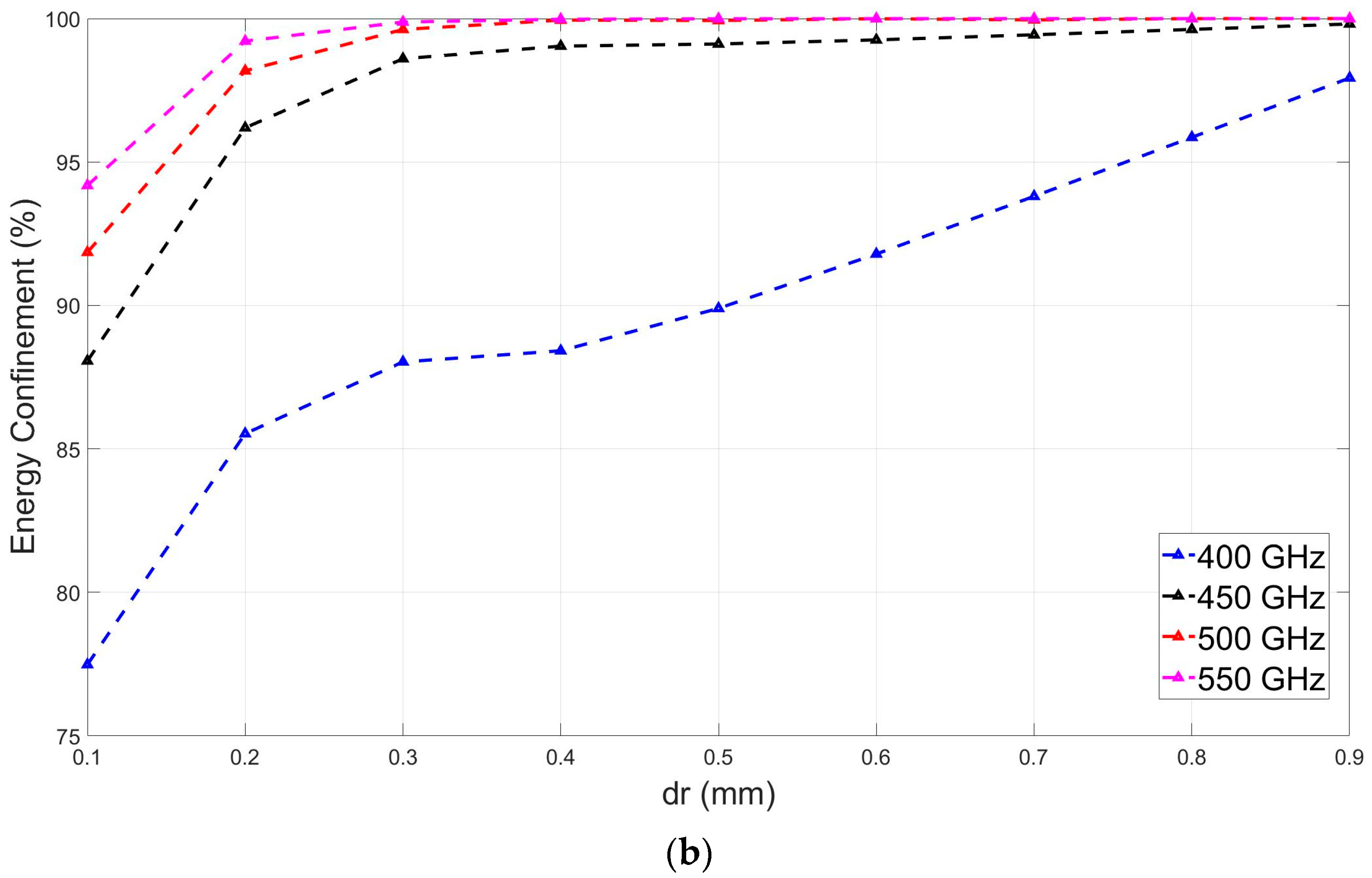
3.2. Energy Confinement

For solid-core polymer dielectric waveguides, the electromagnetic waves are confined to the dielectric rod and the air in its vicinity. If more of the guided energy is distributed outside the dielectric, the loss due to dielectric absorption will be lower, which leads to a lower overall transmission loss. Conversely, if the dielectric waveguide strongly confines the energy, the electromagnetic waves are less likely to escape into free space when bending, which means the dielectric waveguide will have lower bending loss. To investigate what is related to the energy limitation, we defined a virtual circle on the cross-section of the dielectric waveguide with a radius larger than that of the waveguide by a distance of dr, as shown in Figure 2. If the ratio of the transmitted power within this circular region to the total transmitted power is greater than 99%, we consider that most of the energy is confined within the dr range around the dielectric waveguide. Figure 3a shows the energy confinement of electromagnetic waves for dielectric waveguides of different diameters at 500 GHz. Waveguides with larger diameters have a stronger ability to confine electromagnetic waves. Figure 3b shows the energy confinement of the PTFE circular dielectric waveguide with a diameter of 0.5 mm to electromagnetic waves of different frequencies, which indicates that the higher the frequency, the stronger the confinement of the dielectric waveguide to electromagnetic waves. Additionally, for the 0.5 mm diameter PTFE circular dielectric waveguide, within the 450–550 GHz range, the vast majority of the energy is confined within a 1 mm range around the dielectric rod. This is beneficial for determining the thickness of the protective cladding for the dielectric waveguide.

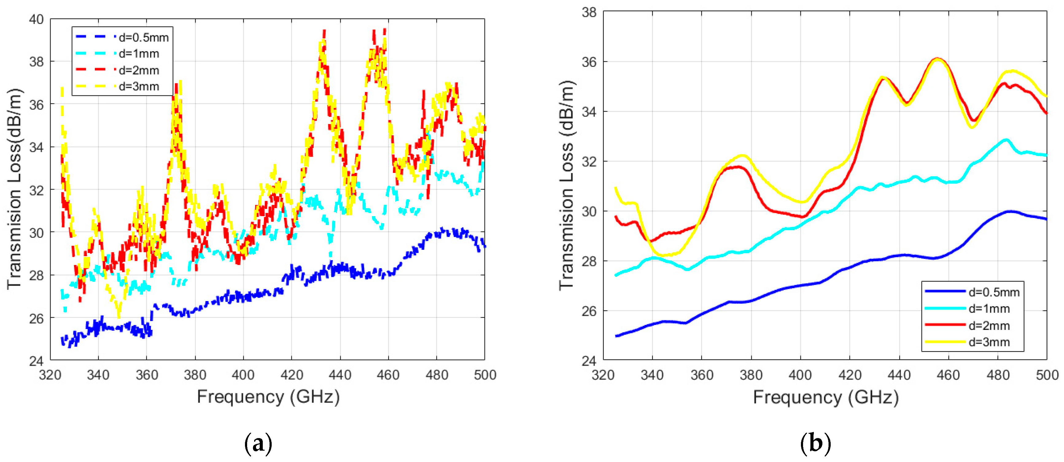
3.3. Transmission Loss
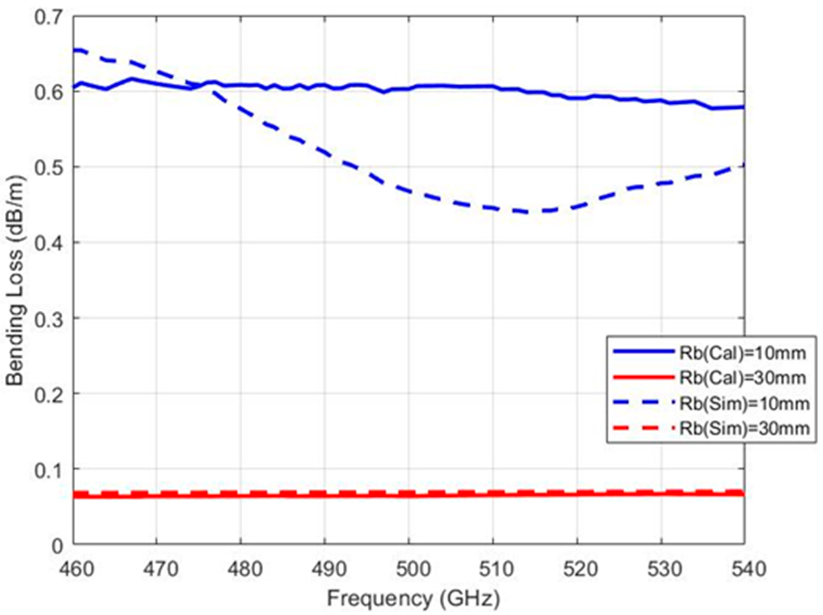
The most important parameter of a dielectric waveguide is the transmission constant, which can be written as follows:
γ = α + j β
where α is the attenuation constant and β is the phase constant. The relationship between the attenuation constant and the transmission loss is, according to [25,28]:
T r a n s m i s s i o n   L o s s d B / m = 20 × log 10 e α
As mentioned earlier, for the 0.5 mm diameter PTFE circular dielectric waveguide operating at 500 GHz, only the HE11 mode is inspired. Since the HE11 mode is derived from the degeneracy of two orthogonal modes with the same propagation constant, only one of them is considered. We will compare the transmission loss calculated from the propagation constant with the loss obtained from full-wave simulation software. For the 1 mm diameter PTFE circular dielectric waveguide, although higher-order modes may be inspired, most of the energy is still transmitted with the fundamental mode HE11. The result is shown in Figure 4. As mentioned in Section 3.2, with higher frequency and larger dielectric waveguide dimensions, the dielectric waveguide has a greater ability to confine electromagnetic waves. Thus, the material absorption loss increased, leading to higher transmission loss, which is consistent with the simulation results. In the frequency range of 460–540 GHz, the PTFE dielectric waveguide has transmission loss of less than 32 dB/m with a diameter of 0.5 mm and less than 34.5 dB/m with a diameter of 1 mm.

3.4. Bending Loss

We use numerical calculations to analyze the bending loss based on the conformal mapping technique [29]. A curved dielectric waveguide is equivalent to a straight dielectric waveguide with the following dielectric constant:
ε r b x , y = ε r x , y e ξ / R b
where ξ = { x , y } is bending direction and Rb is bending radius. In addition, a bent circular dielectric waveguide with a diameter of 0.5 mm was also modeled and simulated by 3D electromagnetic simulation software as a verification, where the bending angle is set to 90°. By subtracting the simulated loss of the bent dielectric waveguide from the simulated loss of a straight waveguide of the same length, we could obtain the additional loss caused by the bending of the dielectric waveguide. The results are shown in Figure 5. A larger bending radius introduces a smaller bending loss because of less structural discontinuity. This situation is closer to the case of straight waveguide transmission. However, as mentioned earlier, the dielectric waveguide has a stronger constraint on electromagnetic waves at higher frequencies. Therefore, the electromagnetic waves are more likely to propagate along the waveguide rather than radiate outward at bends, so the bending loss of the dielectric waveguide is not obvious at frequencies as high as 500 GHz. Even with a bending radius as small as 10 mm, the bending loss does not exceed 1 dB, which is significantly less than the transmission loss of the dielectric waveguide itself. Since it is unlikely to bend the dielectric waveguide with a smaller bending radius in practical engineering applications, the bending loss would not be a major problem.

4. Key Issues in the Practical Use of Dielectric Waveguides
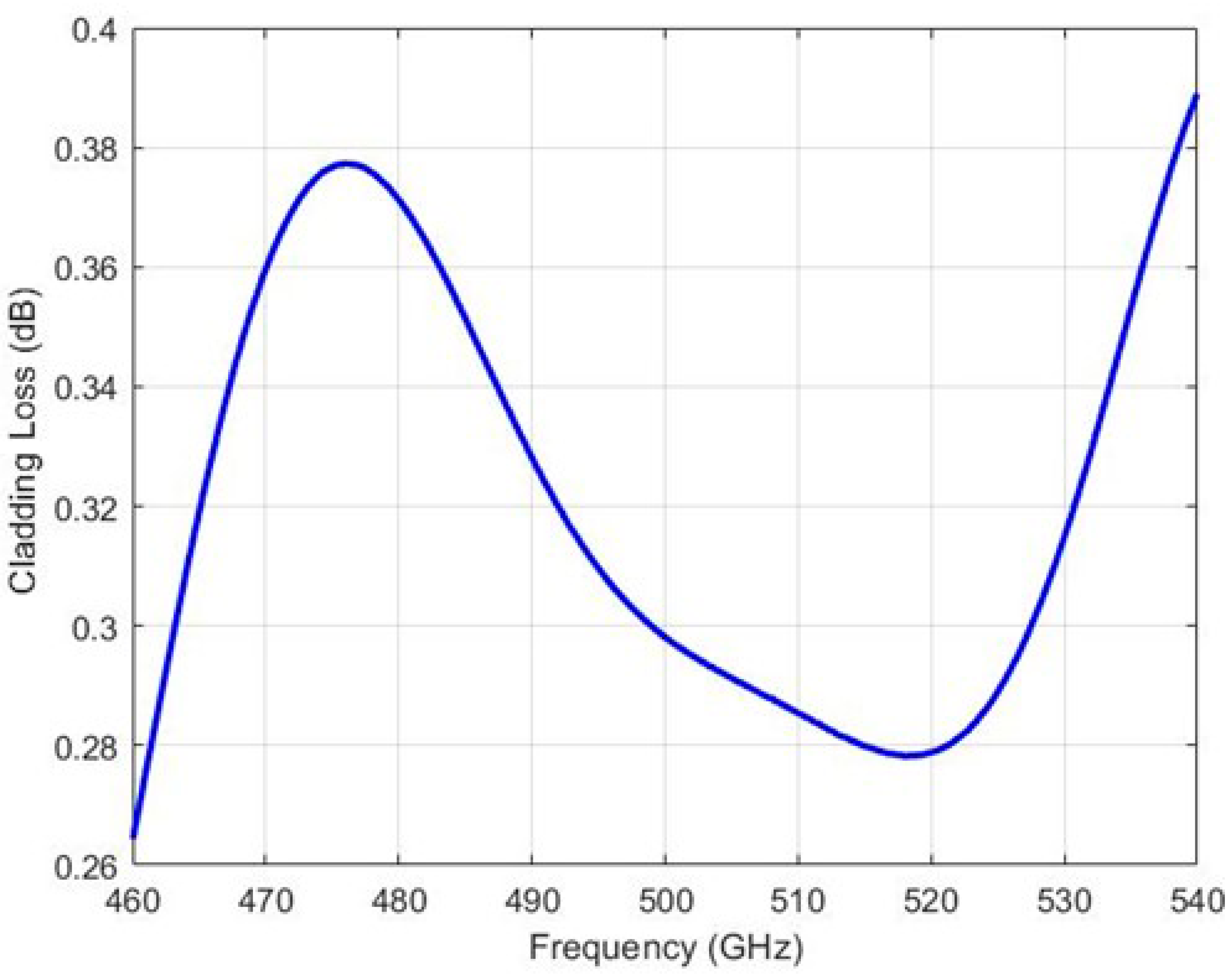
The cladding of dielectric waveguides, mode transmitters from metal waveguides to dielectric waveguides, and interconnection methods between dielectric waveguides are presented. This helps us to integrate dielectric waveguides into measurement systems and facilitate their engineering applications.

4.1. Cladding

As mentioned in Section 3.2, electromagnetic waves are propagated within a 1 mm range around the dielectric waveguide. Environmental interference may cause significant losses or even prevent electromagnetic waves from propagating. Therefore, it is necessary to use cladding material to protect the dielectric waveguide in practical conditions. The added cladding must increase transmission loss as small as possible and try not to impact the mechanical flexibility of the dielectric waveguide. According to [25], expanded polyethylene (EPE) is a suitable cladding material for dielectric waveguides. Due to its loose foam structure, it has a dielectric constant close to air and a low loss tangent. The dielectric constant of the EPE is set to 1.02 and the tangent loss angle to 0.0004. The simulated additional loss introduced by the 2 mm EPE cladding is less than 0.4 dB, as shown in Figure 6.

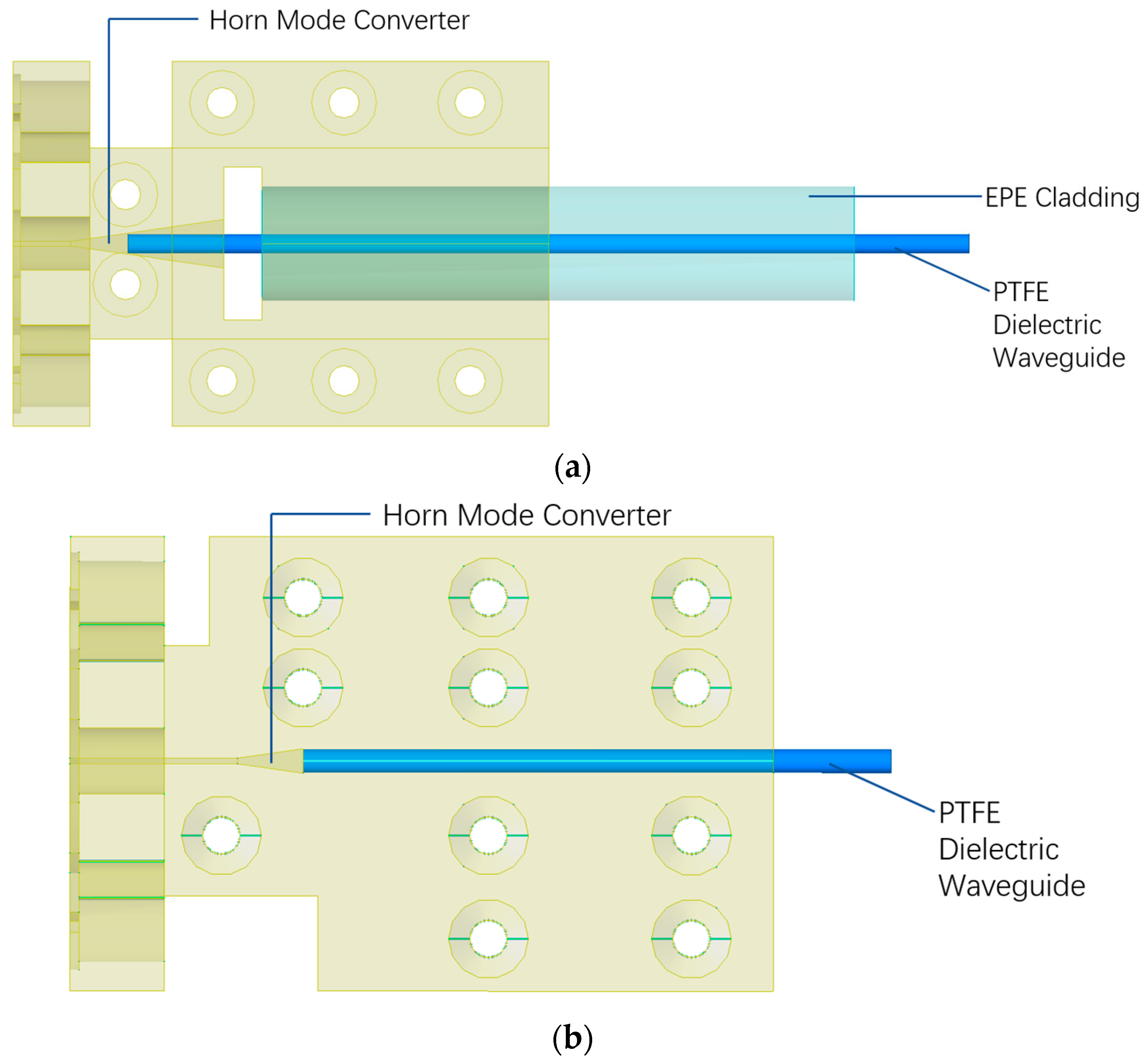
4.2. Metal Waveguide–Dielectric Waveguide Connection

Since the electromagnetic waves will be fed from a metal waveguide, the connection from metal waveguides to dielectric waveguides is important. The electromagnetic waves need to be converted from the TE10 mode in the standard waveguide WR1.9 to the HE11 mode in the dielectric waveguide. A horn structure is used to accomplish the mode conversion, based on which two different mode transmitters are designed.
Mode transmitter 1 features a larger flared opening to accommodate dielectric waveguides of various sizes. The EPE cladding mentioned in Section 4.1 is added to the outside of the dielectric waveguide. By applying adhesive to the exterior of the cladding, a strong connection with the metal mode transmitter is realized. Since the cladding thickness exceeds the region where the electromagnetic waves propagate outside the dielectric waveguide, this will not affect the performance of the dielectric waveguide. However, due to the possible displacement between the dielectric waveguide and the cladding, the insertion loss may deteriorate.
In mode transmitter 2, the horn opening is designed to be the same size as the diameter of the dielectric waveguide and connect to a cavity that matches the waveguide’s diameter. The mode transmitter is manufactured into two split blocks by Computer Numerical Control (CNC) milling. By clamping the dielectric between the upper and lower halves, the dielectric waveguide could connect tightly with the mode transmitter.
The models of the two mode transmitters are shown in Figure 7a,b. Mode transmitter 1 is suitable for preliminary observation due to its ability to accommodate dielectric waveguides of different sizes. Mode transmitter 2, on the other hand, is designed to fit only one specific size of dielectric waveguide but offers lower insertion loss and a tight connection. We simulated the S parameter for the tight connection condition as well as for offsets of 3 mm and 6 mm from the ideal connection position, as shown in Figure 8, where insertion loss and return loss is expressed. In practical operation, minor displacements of the dielectric waveguide do not result in a significant increase in insertion loss.

4.3. Interconnection between Dielectric Waveguides

In practical engineering, it is often necessary to use different lengths of dielectric waveguides. Connecting two dielectric waveguides to a longer one can enhance the ease of use. We used a Teflon heat-shrinkable tube with an inner diameter of 0.5 mm and an outer diameter of 0.9 mm as the connector. The force generated by heat shrinking can connect two short dielectric waveguides tightly. The whole structure can be regarded as a 0.5 mm diameter dielectric waveguide with a 0.9 mm diameter section in the middle, as shown in Figure 9. Simulation results shown in Figure 10 indicate the interconnector’s insertion loss ranges from 1.16 to 2.34 dB in the 460–540 GHz frequency range, increasing with frequency. Teflon heat-shrinkable tube is easy to obtain and can adapt to different sizes of dielectric waveguides, so it is feasible to be used as a low-cost and convenient interconnector.

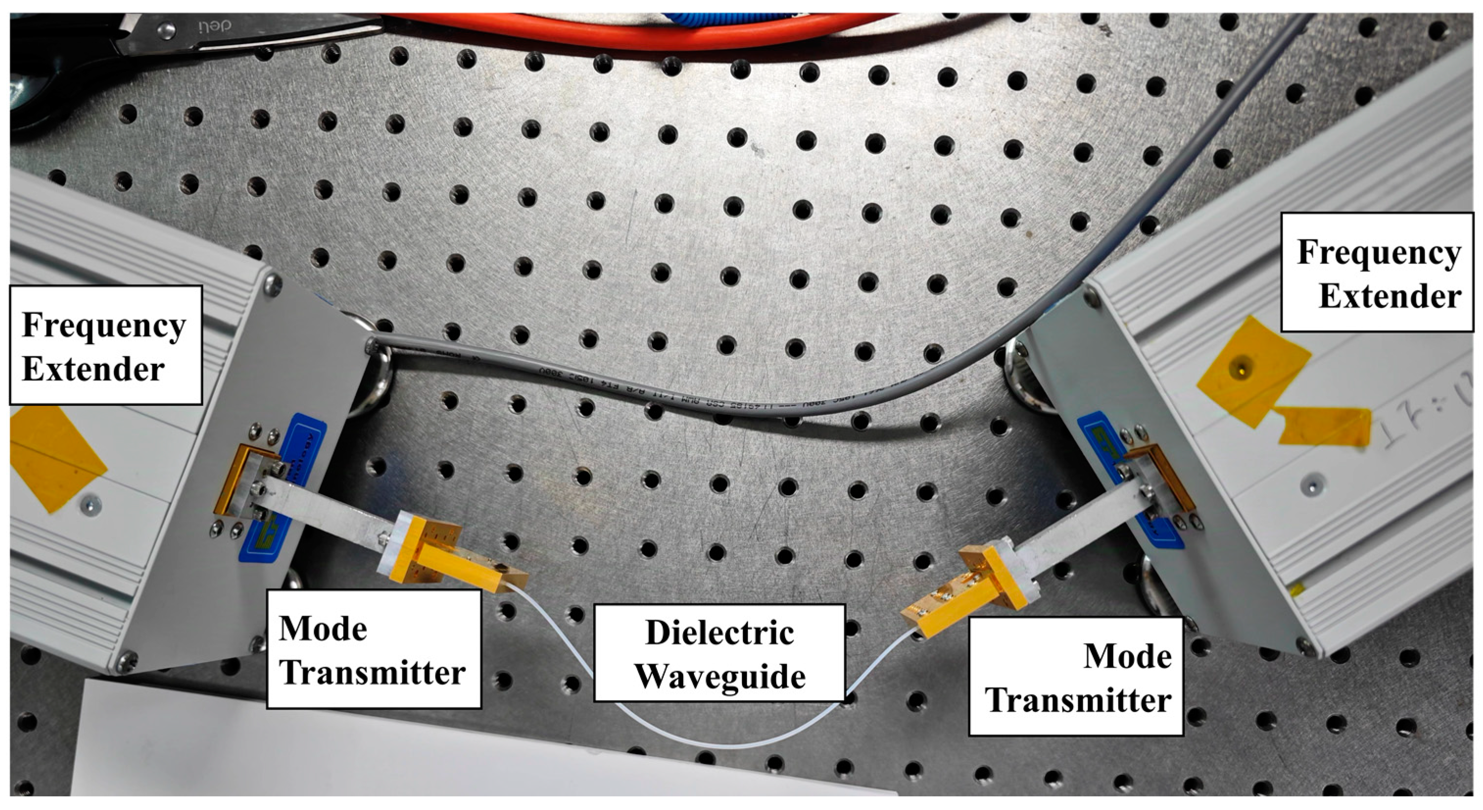
5. Measurement and Result

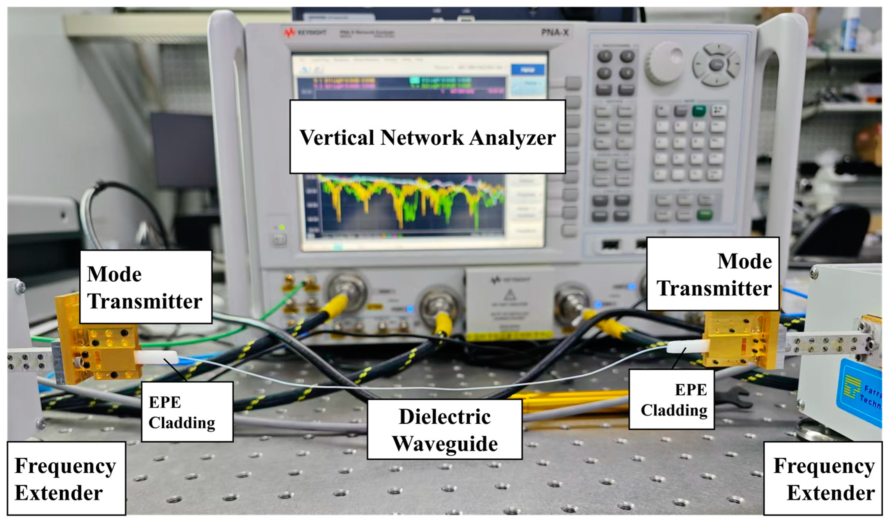
5.1. Measurement Settings

We measured the dielectric waveguide using a vector network analyzer (VNA) and frequency extenders in the frequency range of 325–500 GHz. The schematic of the measurement system is shown in Figure 11. The dielectric waveguide is connected via the mode transmitters mentioned in 4.2 to the two frequency extender modules, while the S parameter is read by the vector network analyzer. The two frequency extender modules are slightly misaligned to prevent electromagnetic waves from directly coupling through free space to the other end. By measuring the insertion loss of dielectric waveguides with different lengths, the transmission loss of the dielectric waveguide can be obtained by the de-embedding method. It is worth mentioning that the waveguide port used in our mode transmitter is WR1.9 (0.48 × 0.24 mm) to facilitate the subsequent system application, while the waveguide port of the frequency extender is WR2.2 (0.56 × 0.28 mm). This mismatch introduces additional standing waves and transmission losses. Figure 12 shows photographs of the dielectric waveguides and associated components to be measured, including the mode transmitters, the EPE cladding, and the heat-shrinking tube for interconnection of dielectric waveguides.

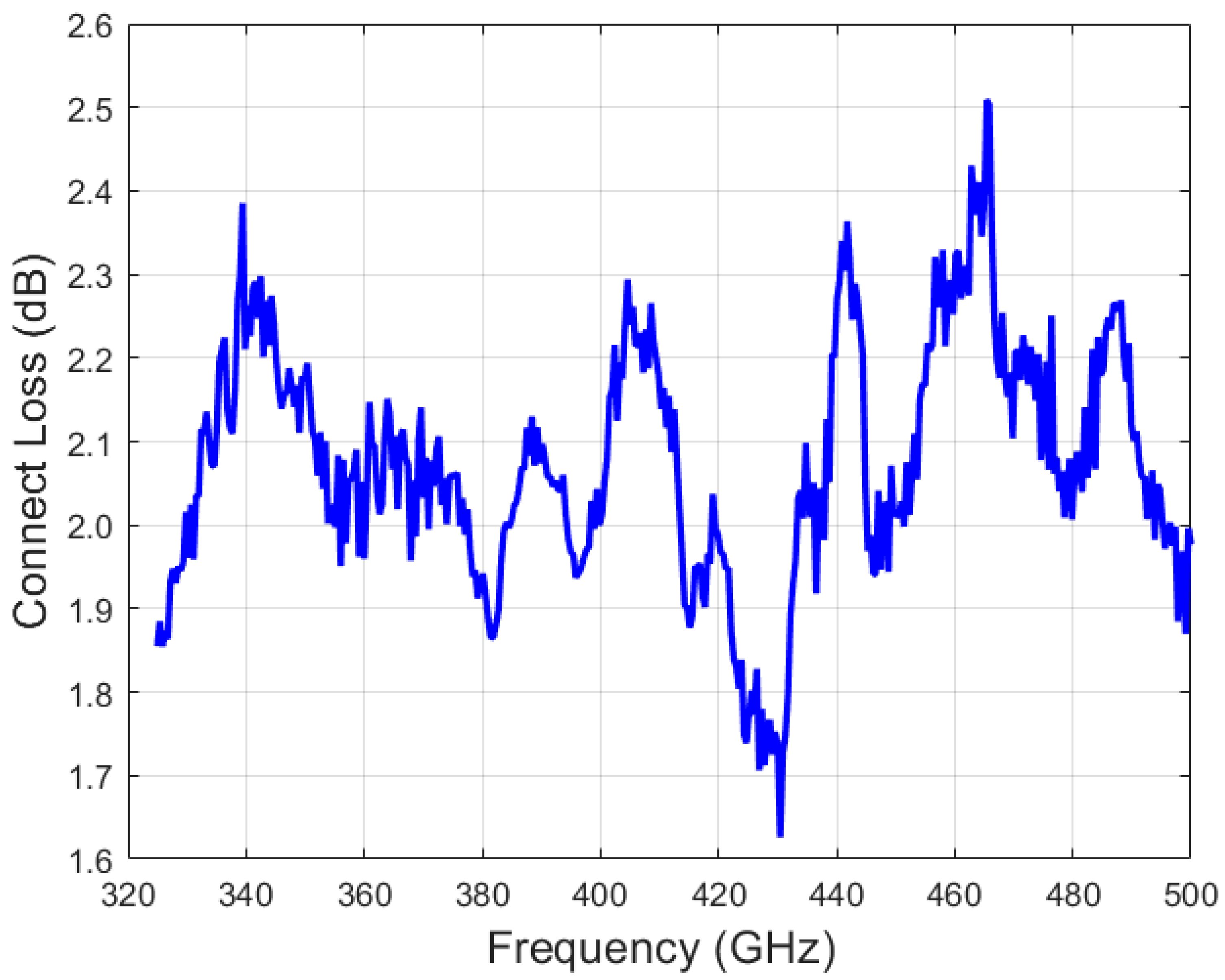
5.2. Transmission Loss
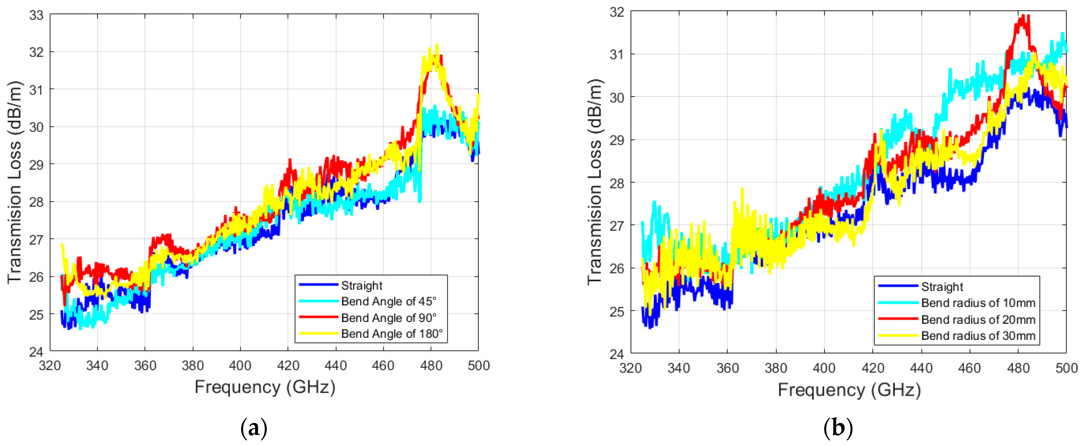
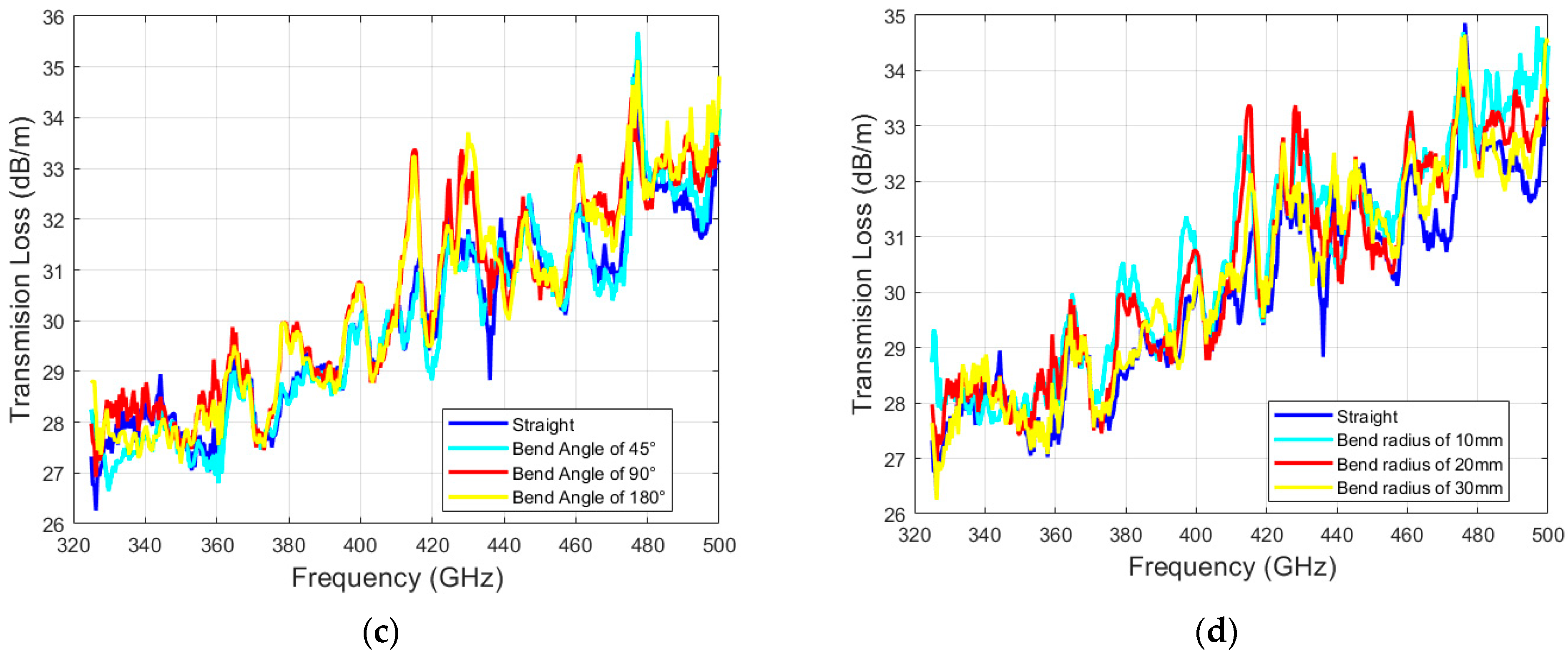
We measured dielectric waveguides with diameters of 0.5 mm, 1 mm, 2 mm, and 3 mm using mode transmitter 1. For each size of dielectric waveguide, the length was taken as 10 mm and 3 0 mm, and the ends of the dielectric waveguide were connected as tightly as possible to the mode transmitter through a cut EPE cladding, as shown in Figure 13. The transmission loss obtained through the de-embedding method is shown in Figure 14. The original data are shown in (a). To make the trends more visually apparent, we applied a smoothing process to the data, as shown in (b). As the frequency increases and the diameter of the dielectric waveguide grows, the transmission loss of the waveguide increases, which is consistent with our previous analysis and simulation results. Additionally, the larger diameter of the dielectric waveguide could excite higher-order modes, leading to additional losses. Overall, the transmission loss for the 0.5 mm diameter dielectric waveguide is less than 30 dB/m, while the transmission loss for the 1 mm diameter waveguide is less than 33 dB/m.

5.3. Bending Loss

We measured the bending loss of dielectric waveguides with diameters of 0.5 mm and 1 mm using mode transmitter 2, as shown in Figure 15. Due to the tighter connection of mode transmitter 2 to the dielectric waveguide as mentioned above, it is less sensitive to possible displacements. Thus, it can ensure measurement accuracy when the dielectric waveguide is bent with different radii of curvature and angles. Figure 16a–d show the losses measured for dielectric waveguides with diameters of 0.5 mm and 1 mm bent 45°, 90°, and 180° at a bending radius of 20 mm, as well as bent 90° at bending radii of 10 mm, 20 mm, and 30 mm. As the bending angle and bending radius increase, the bending loss also gets larger, which agrees with our simulation results. However, even with a bending radius of 10 mm, the additional bending loss is only about 1 dB/m, which is much smaller than the transmission loss. As previously analyzed, in the high-frequency range around 500 GHz, due to the strong electromagnetic-wave-confining ability of dielectric waveguides, the bending loss is not significant.

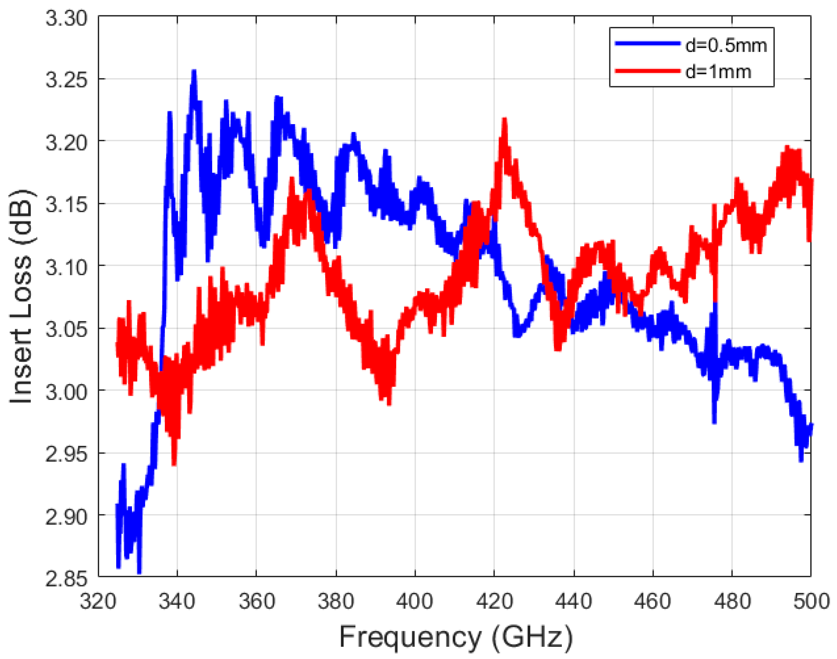
5.4. Insertion Loss of the Mode Transmitter

By subtracting the loss of the dielectric waveguide from the overall system loss, we can obtain the insertion loss of the mode transmitter. Since the loss of mode transmitter 1 varies with different sizes of dielectric waveguides, we only calculate the insertion loss of mode transmitter 2 here. The insertion loss ranges from 2.85 to 3.25 dB, slightly higher than the simulation results, as shown in Figure 17. This may be due to possible surface oxidation and roughness of the physical processing, as well as the mismatch between the waveguide ports as mentioned before

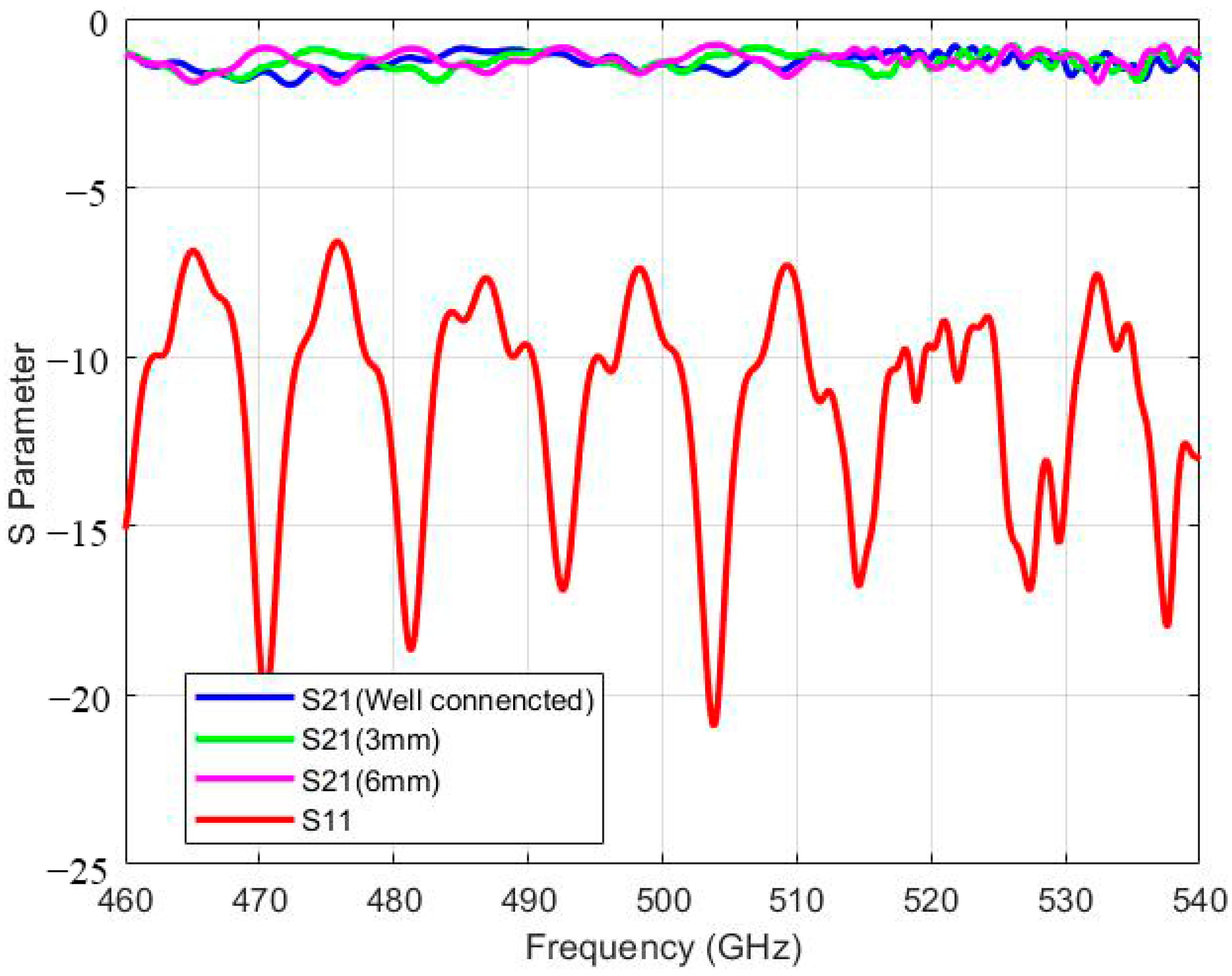
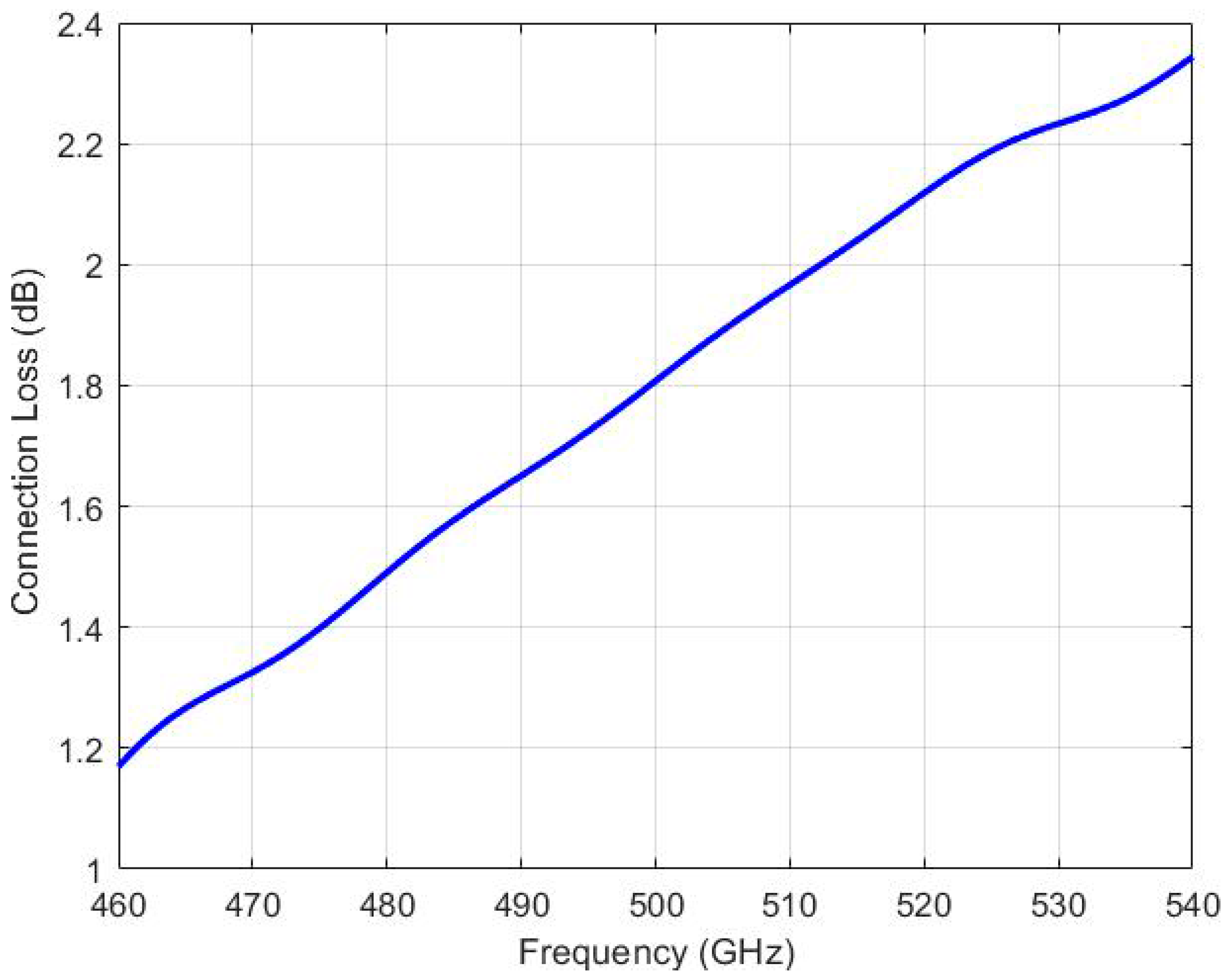
5.5. Interconnection between Dielectric Waveguides

We connected two dielectric waveguides with a diameter of 0.5 mm and a length of 10 mm with a heat-shrink tube and measured the transmission loss. By comparing this result with the transmission loss of a dielectric waveguide with a diameter of 0.5 mm and a length of 20 mm, we can calculate the additional loss caused by the interconnection. As shown in Figure 18, the additional loss ranges from 1.6 to 2.5 dB, which is slightly higher than the simulation. The cut surfaces of the two connected dielectric waveguides may not perfectly match, leading to a less tight connection. Considering that it offers low cost, ease of operation, and adaptability to different sizes of dielectric waveguides, using PTFE heat-shrink tubes for temporary interconnection is a feasible approach.

6. Conclusions

In this paper, we designed, fabricated, and measured solid-core polymer dielectric waveguides with an operating range as high as 500 GHz. By measuring the dielectric constants and loss tangents of various polymer materials in the frequency range of 325–500 GHz, we chose PTFE as the material for our dielectric waveguides. Through theoretical analysis, simulation, and experiments, we analyzed and verified how the diameter of dielectric waveguides and the operating frequency influence properties such as transmission loss and bending loss. Additionally, we designed and discussed the cladding for the dielectric waveguides, the mode transmitter between metal waveguides and dielectric waveguides, and the interconnection method between dielectric waveguides.
The main contributions of this paper are as follows: (1) We measured the electrical properties of polymers in the 325–500 GHz range, providing a reference for future research. (2) There is not much research on solid-core polymer dielectric waveguides operating at 500 GHz. In this paper, PTFE dielectric waveguides with diameters of 0.5 mm and 1 mm are designed, fabricated, and measured. The transmission loss is less than 30 dB/m and 33 dB/m, respectively, and the bending loss is less than 1 dB/m in the frequency range of 325–500 GHz. These waveguides have potential application value in short-range communication and non-destructive testing. (3) This paper presents low-cost and easy-to-operate interconnections of dielectric waveguides by using PTFE heat-shrink tubes, which have practical value in engineering.

Author Contributions

Conceptualization, H.L., D.Z. and H.Z; methodology, H.L.; validation, H.L.; formal analysis, H.L.; investigation, H.L.; resources, D.Z.; data curation, H.L.; writing—original draft preparation, H.L.; writing—review and editing, H.Z.; visualization, H.L.; supervision, D.Z.; project administration, D.Z.; funding acquisition, D.Z. All authors have read and agreed to the published version of the manuscript.

Funding

This research was funded by the Youth Innovation Promotion Association CAS, grant number E1213A041S.

Institutional Review Board Statement

Not applicable.

Informed Consent Statement

Not applicable.

Data Availability Statement

The data that support the findings of this study are available from the corresponding author upon reasonable request.

Acknowledgments

The author would like to appreciate Yang Yu for his assistance for the experiment.

Conflicts of Interest

The authors declare no conflicts of interest.

References

  1. Siegel, P.H. Terahertz technology. IEEE Trans. Microw. Theory Tech. 2002, 50, 910–928. [Google Scholar] [CrossRef]
  2. Sleiman J, B. Terahertz Imaging and Spectroscopy: Application to Defense and Security in Front of the Examination Panel. Ph.D. Thesis, Université de Bordeaux, Bordeaux, French, 2016. [Google Scholar]
  3. Burford, N.M.; El-Shenawee, M.O.; Neal, C.B.O.; Olejniczak, K.J. Terahertz Imaging for Nondestructive Evaluation of Packaged Power Electronic Devices. Int. J. Emerg. Technol. Adv. Eng. 2014, 4, 395–401. [Google Scholar]
  4. Piesiewicz, R.; Kleine-Ostmann, T.; Krumbholz, N.; Mittleman, D.; Koch, M.; Schoebel, J.; Kurner, T. Short-Range Ultra-Broadband Terahertz Communications: Concepts and Perspectives. IEEE Antennas Propag. Mag. 2007, 49, 24–39. [Google Scholar] [CrossRef]
  5. Ducournau, G.; Szriftgiser, P.; Pavanello, F.; Peytavit, E.; Zaknoune, M.; Bacquet, D.; Beck, A.; Akalin, T.; Lampin, J.-F.; Lampin, J.-F. THz Communications using Photonics and Electronic Devices: The Race to Data-Rate. J. Infrared Millim. Terahertz Waves 2015, 36, 198–220. [Google Scholar] [CrossRef]
  6. Ducournau, G.; Pavanello, F.; Beck, A.; Tohme, L.; Blin, S.; Nouvel, P.; Peytavit, E.; Zaknoune, M.; Szriftgiser, P.; Lampin, J.F. High-definition television transmission at 600 GHz combining THzphotonics hotspot and high-sensitivity heterodyne receiver. Electron. Lett. 2014, 50, 413–415. [Google Scholar] [CrossRef]
  7. Katyba, G.M.; Zaytsev, K.I.; Dolganova, I.N.; Chernomyrdin, N.V.; Ulitko, V.E.; Rossolenko, S.N.; Shikunova, I.A.; Kurlov, V.N. Sapphire waveguides and fibers for terahertz applications. Prog. Cryst. Growth Charact. Mater. 2021, 67, 100523. [Google Scholar] [CrossRef]
  8. Barh, A.; Pal, B.P.; Agrawal, G.P.; Varshney, R.K.; Rahman, B.M.A. Specialty Fibers for Terahertz Generation and Transmission: A Review. IEEE J. Sel. Top. Quantum Electron. 2016, 22, 365–379. [Google Scholar] [CrossRef]
  9. Islam, M.S.; Cordeiro, C.M.; Franco, M.A.; Sultana, J.; Cruz, A.L.; Abbott, D. Terahertz optical fibers. Opt. Express 2020, 28, 16089–16117. [Google Scholar] [CrossRef]
  10. Mitrofanov, O.; James, R.; Fernández, F.A.; Mavrogordatos, T.K.; Harrington, J.A. Reducing transmission losses in hollow THz waveguides. IEEE Trans. Terahertz Sci. Technol. 2011, 1, 124–132. [Google Scholar] [CrossRef]
  11. Geiger, M.; Hitzler, M.; Saulig, S.; Iberle, J.; Hügler, P.; Waldschmidt, C. A 160-GHz radar with flexible antenna used as a sniffer probe. IEEE Sens. J. 2017, 17, 5104–5111. [Google Scholar] [CrossRef]
  12. Hondros, D.; Debye, P. Electromagnetische wellen in dielektrischen drahtes. Ann. Der Phys. 1910, 32, 465. [Google Scholar] [CrossRef]
  13. Agrawal, G.P. Fiber-Optic Communication Systems, 3rd ed.; John Wiley & Sons, Inc.: Hoboken, NJ, USA, 2002. [Google Scholar]
  14. Argyros, A. Microstructures in polymer fibres for optical fibres, terahertz waveguides, and fibre-based metamaterials. ISRN Opt. 2013, 2013, 785162. [Google Scholar] [CrossRef]
  15. Knight, J.C.; Broeng, J.; Birks, T.A.; Russel, P.S.J. Photonic band gap guidance in optical fibers. Science 1998, 282, 1476–1478. [Google Scholar] [CrossRef] [PubMed]
  16. Russell, P. Photonic crystal fibers. Science 2003, 299, 358–362. [Google Scholar] [CrossRef]
  17. Knight, J.C. Photonic crystal fibres. Nature 2003, 424, 847–851. [Google Scholar] [CrossRef]
  18. Mei, S.; Kong, D.; Wang, L.; Ma, T.; Zhu, Y.; Zhang, X.; He, Z.; Huang, X.; Zhang, Y. Suspended graded-indexporous core POF for ultra-flat near-zero dispersion terahertz transmission. Opt. Fiber Technol. 2019, 52, 101946. [Google Scholar] [CrossRef]
  19. Couny, F.; Benabid, F.; Roberts, P.J.; Light, P.S.; Raymer, M.G. Generation and photonic guidance of multi-octaveoptical-frequency combs. Science 2007, 318, 1118–1121. [Google Scholar] [CrossRef]
  20. Sultana, J.; Islam, M.S.; Cordeiro, C.M.B.; Dinovitser, A.; Koushik, M.; Ng, B.W.-H.; Abbott, D. Terahertzhollow core antiresonant fiber with metamaterial cladding. Fibers 2020, 8, 14. [Google Scholar] [CrossRef]
  21. Chen, L.J.; Chen, H.W.; Kao, T.F.; Lu, J.Y.; Sun, C.K. Low-loss subwavelength plastic fiber for terahertz waveguiding. Opt. Lett. 2006, 31, 308–310. [Google Scholar] [CrossRef]
  22. Dolatsha, N.; Saiz, N.; Arbabian, A. Fully packaged millimetre-wave dielectric waveguide with multimodal excitation. Electron. Lett. 2015, 51, 1339–1341. [Google Scholar] [CrossRef]
  23. Dey, U.; Hesselbarth, J. Millimeter-wave Chip-to-Chip Interconnect Using Plastic Wire Operating in Single and Dual Mode. In Proceedings of the 2018 IEEE/MTT-S International Microwave Symposium—IMS, Philadelphia, PA, USA, 10–15 June 2018; pp. 1549–1552. [Google Scholar] [CrossRef]
  24. Nallappan, K.; Cao, Y.; Xu, G.; Guerboukha, H.; Nerguizian, C.; Skorobogatiy, M. Dispersion-limited versus power-limited terahertz communication links using solid core subwavelength dielectric fibers. Photonics Res. 2020, 8, 1757–1775. [Google Scholar] [CrossRef]
  25. Li, Y.; Liao, S.; Xue, Q.; Che, W. Transmission Characteristics of Flexible Low-Loss Solid Circular Polymer Dielectric Waveguides for Sub-THz Applications. J. Infrared Millim. Terahertz Waves 2023, 44, 110–133. [Google Scholar] [CrossRef]
  26. Chen, H.; Chen, H.; Zhang, C.; Che, W.; Xue, Q. Sub-terahertz Dual-polarized Low-loss Transmission System Using COC-Based Dielectric Waveguide. J. Infrared Millim. Terahertz Waves 2024, 45, 141–158. [Google Scholar] [CrossRef]
  27. Zhu, H.T.; Wu, K. Complex permittivity measurement of dielectric substrate in sub-THz range. IEEE Trans. Terahertz Sci. Technol. 2020, 11, 2–15. [Google Scholar] [CrossRef]
  28. Yeh, C.; Shimabukuro, F.I. The Essence of Dielectric Waveguides; Springer: New York, NY, USA, 2008. [Google Scholar]
  29. Olszewski, J.; Szpulak, M.; Urbanczyk, W. Effect of coupling between fundamental and cladding modes on bending losses in photonic crystal fibers. Opt. Express 2005, 13, 6015–6022. [Google Scholar] [CrossRef]
Figure 1. The relationship between the effective refractive index of different modes and the diameter of the dielectric rod is shown. The working frequency is 500 GHz, and a mode is considered to be propagating if its effective refractive index is greater than 1.
Photonics 11 00921 g001
Figure 2. Schematic diagram of the energy confinement simulation setup.
Photonics 11 00921 g002
Figure 3. The simulation result of energy confinement. (a) The energy confinement of PTFE dielectric waveguides of different sizes at a frequency of 500 GHz. (b) The energy confinement of the 0.5 mm diameter PTFE dielectric waveguide under different frequencies.
Photonics 11 00921 g003aPhotonics 11 00921 g003b
Figure 4. Calculated and simulated transmission loss of fundamental mode of PTFE circular dielectric waveguides with diameters of 0.5 mm and 1 mm.
Photonics 11 00921 g004
Figure 5. Calculated and simulated bending loss for 0.5 mm diameter PTFE circular dielectric waveguides with different bending radii.
Photonics 11 00921 g005
Figure 6. Simulated cladding loss for 2 mm EPE cladding.
Photonics 11 00921 g006
Figure 7. Simulated cladding loss for 2 mm EPE cladding. (a) Layout of mode transmitter 1. (b) Layout of mode transmitter 2.
Photonics 11 00921 g007
Figure 8. Simulated S parameter of the horn mode transmitter structure.
Photonics 11 00921 g008
Figure 9. Schematic diagram of interconnector using PTFE heat-shrinkable tube.
Photonics 11 00921 g009
Figure 10. Simulated connection loss of interconnector using PTFE heat-shrinkable tube.
Photonics 11 00921 g010
Figure 11. Schematic of the measurement system.
Photonics 11 00921 g011
Figure 12. Photographs of the dielectric waveguides and associated components.
Photonics 11 00921 g012
Figure 13. Photographs of the measurement system.
Photonics 11 00921 g013
Figure 14. Measured result of transmission of dielectric waveguides: (a) original data; (b) smoothed data.
Photonics 11 00921 g014
Figure 15. Photographs of the measurement system for bent waveguides.
Photonics 11 00921 g015
Figure 16. Measured result of transmission loss of bent dielectric waveguides. (a) Dielectric waveguides with a diameter of 0.5 mm and a bending radius of 20 mm at different bending angles. (b) Dielectric waveguides with a diameter of 0.5 mm and a bending angle of 90° at different bending radii. (c) Dielectric waveguides with a diameter of 1 mm and a bending radius of 20 mm at different bending angles. (d) Dielectric waveguides with a diameter of 1 mm and a bending angle of 90° at different bending radii.
Photonics 11 00921 g016aPhotonics 11 00921 g016b
Figure 17. Measured insertion loss of the mode transmitter.
Photonics 11 00921 g017
Figure 18. Measured connection loss of the interconnector.
Photonics 11 00921 g018
Table 1. Performance of terahertz solid-core dielectric waveguides.
Ref.Working Frequency
(GHz)
Transmission Loss (dB/m)Material
[22]753PE
[23]62–1031.4–6HDPE
[24]1281.01–2.4PTFE
[25]88–1400.5–4.8PP
[26]90–1002.33PTFE
Table 2. Measured results of electrical properties of polymer materials (325–500 GHz).
MaterialDielectric ConstantLoss Tangent
PMMA2.590.02
HDPE2.360.0003
PC2.740.015
PP2.260.0004
PTFE2.070.0004
Disclaimer/Publisher’s Note: The statements, opinions and data contained in all publications are solely those of the individual author(s) and contributor(s) and not of MDPI and/or the editor(s). MDPI and/or the editor(s) disclaim responsibility for any injury to people or property resulting from any ideas, methods, instructions or products referred to in the content.

