Article

Efficient Inverse Design of Large-Scale, Ultrahigh-Numerical-Aperture Metalens

1
State Key Laboratory of Optoelectronic Materials and Technologies, School of Physics, Sun Yat-sen University, Guangzhou 510275, China
2
Guangdong Provincial Key Laboratory of Quantum Metrology and Sensing, School of Physics and Astronomy, Sun Yat-sen University, Zhuhai 519080, China
*
Author to whom correspondence should be addressed.
Photonics 2024, 11(10), 940; https://doi.org/10.3390/photonics11100940
Submission received: 24 September 2024 / Revised: 3 October 2024 / Accepted: 5 October 2024 / Published: 6 October 2024
(This article belongs to the Special Issue Micro-Nano Optical Devices)

Abstract

:
Efficient design methods for large-scale metalenses are crucial for various applications. The conventional phase-mapping method shows a weak performance under large phase gradients, thus limiting the efficiency and quality of large-scale, high-numerical-aperture metalenses. While inverse design methods can partially address this issue, existing solutions either accommodate only small-scale metalenses due to high computational demands or compromise on focusing performance. We propose an efficient large-scale design method based on an optimization approach combined with the adjoint-based method and the level-set method, which first forms a one-dimensional metalens and then extends it to two dimensions. Taking fabrication constraints into account, our optimization method for large-area metalenses with a near-unity numerical aperture (NA = 0.99) has improved the focusing efficiency from 42% to 60% in simulations compared to the conventional design method. Additionally, it has reduced the deformation of the focusing spot caused by the ultrahigh numerical aperture. This approach retains the benefits of the adjoint-based method while significantly reducing the computational burden, thereby advancing the development of large-scale metalenses design. It can also be extended to other large-scale metasurface designs.

1. Introduction

Optical metasurfaces are thin optical components composed of meta-atoms with various shapes and topologies, capable of generating desired phase, amplitude, and polarization distributions in both the near field and far field. This enables them to achieve a variety of extraordinary optical phenomena, including lensing [1,2,3], beam deflection [4,5], holography [6,7], and more [8,9]. Recent advancements in metasurfaces have gained significant importance across a wide range of scientific and technological fields, including communications [10], sensing [11], imaging [12,13], and optical computing [14,15]. Metalenses, in particular, are among the most promising optical elements for practical applications, as they significantly reduce the cost, complexity, and form factor of imaging systems.
Currently, most metalenses are designed using a phase-mapping approach [1]. In this conventional design method, each meta-atom is viewed as part of a periodic array and placed into equally spaced units. However, this design method has several limitations that lead to a weak performance in metalenses with high numerical apertures (NAs). First, in the design of high-NA metalenses, a discretized phase profile is insufficient to replicate a continuous profile accurately. Theoretically, the size of the meta-atoms must satisfy the Nyquist sampling criterion, requiring them to be small enough for high-NA metalenses [16]. This makes fabrication more challenging. Second, the “local periodicity” approximation fails when there are rapidly varying meta-atoms or structures with lower refractive indices or smaller intervals, leading to stronger coupling among meta-atoms. As a result, there is a significant difference between the actual response of the meta-atoms within the metalenses and the ideal response of the meta-atoms in a periodic array, which may reduce the focal efficiency [17].
Heuristic optimization can help us find a suitable combination of parameters compared to the global search method. However, limited by the computational cost and convergence rate of the algorithm, this method is typically applied to structures represented by only a few parameters, such as thickness or shape parameters. Due to the same reason, the size of the structures designed using this method tends to be relatively small or simple. Even when applied to the design of a small one-dimensional metalens [18], the optimization area must be expanded gradually to reduce the difficulty of optimization. As a result, heuristic optimization is often used as a supplement to the phase-mapping approach to improve the performance [19], while it is weak in designing large-scale meta devices.
The adjoint-based method is a widely used inverse design technique. Since each iteration can efficiently calculate the gradient of each parameter with only two simulations, the forward and adjoint processes, it significantly increases the number of design variables [20]. This enables the creation of complex shapes that push performance limits further and allows for the optimization of the entire metalens [21], regulating meta-atom coupling to enhance overall performance. However, the complex shapes generated by the adjoint-based method are difficult to fabricate, and the high computational cost of electromagnetic simulations limits the size of the metalens. Although some recent studies use more regular shapes or incorporate approximations to reduce simulation costs [22], these compromises often come at the expense of optical performance. Using the adjoint-based method for metagrating design can partially alleviate the simulation area limitations [23]. However, due to the significant variation in the metagrating period across the metalens for different deflection angles, it is often necessary to divide the metalens into regions and fine-tune each structure for higher efficiency, thus greatly complicating the design process. Recently, the supercell approach, combined with the adjoint-based method, divides the metalens into several linear scatters for optimization to enable broader applications [24,25]. However, deviation from complex wavefront and the increased number of scatters for large-scale structures make the design process more complicated.
To address the challenge of designing large-scale metalenses, we present a new strategy that significantly accelerates the design process and improves the focusing performance of large-scale, ultrahigh-NA metalenses. We utilize an adjoint-based level-set optimization method to optimize a one-dimensional metalens, which is then extended to a two-dimensional metalens by leveraging the symmetry of the metalens. As a result, it makes the computational cost scale linear with the radius, whereas it scaled with the metalens area in previous methods. Compared to the metagrating design [23,26], our approach eliminates the restriction of Fresnel zones without significantly increasing computational costs. As proof of concept, we designed a metalens with a near-unity NA (NA = 0.99) operating at a wavelength of 1050 nm. The focusing efficiency increased from 42% in the conventional design to 60% in our optimized design. Additionally, the deformation of the focal spot in our optimized metalens was smaller than that of both the conventional and metagrating-designed metalenses. Our design method not only significantly reduces computational costs but also avoids introducing serious constraints, showing the potential for future large-scale metalens designs.

2. Methods

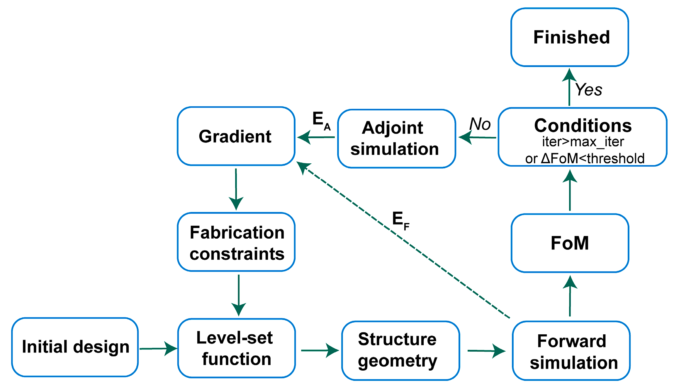
2.1. Adjoint-Based Level-Set Optimization Method

Metasurface design involves determining a set of structural parameters that efficiently transform incident wavefronts into target output wavefronts. As shown in Figure 1, the design process begins with an initialization and then iteratively refines the structures to maximize the figure of merit (FoM) [20].
To quantify the fidelity of the output field, the FoM is typically defined as the fraction of the output field that matches the desired field distribution at the FoM plane [22]:
F o M = F 2 = S E d * · E f d A 2 ,
where E d * represents the complex conjugate of the desired field at the FoM plane, E f is the output field of the structure at the FoM plane, and F is the complex-valued projection of E f and E d . The output field is realized through forward simulation, excited by a preset input field. To increase the FoM, the adjoint simulation complements the forward simulation by evaluating the impact of structural boundaries and calculating the gradient of all structural parameters.
To better represent the structure design, the level-set method is a powerful tool [27,28]. The level-set method leverages degrees of design freedom, using fewer parameters to build more complex structures compared to regular or pixelated shapes. It represents two-dimensional shapes through the intersection of the contour of a three-dimensional function with a plane. By combining the adjoint-based method with the level-set method, high-performance metasurfaces featuring continuous, clear boundaries and complex shapes are designed [29,30,31]. Considering the Hamilton–Jacobi partial differential equation, which governs the deformation of the level-set function, and the gradient of the adjoint-based method, the gradient of the structural parameters can be regarded as follows [20]:
F o M p = 2 Re F * B ( ε 2 ε 1 ) ϕ p 1 ϕ E f · E a + 1 ε 1 ε 2 D f · D a d A ,
where p is the variable in the level-set function, ϕ ; ε 1 and ε 2 are the permittivity of the cladding material (air) and high-index dielectric material of the structure; B is the side interfaces of the structure; E f and D f are the tangential component of the electric field and normal component of the electric displacement field at interfaces in the forward simulation; and E a and D a are the corresponding components of fields in the adjoint simulation. The fields distribution on the interfaces are interpolated from points on the Yee grid using a bilinear approach to eliminate inaccurate data from the boundary across several grids [22,32].
Different from the level-set functions usually based on signed distance function [31,33] or norms [34], here we design the level-set function in a polynomial form. The complexity of shape can be adjusted by controlling the number of items in the Fourier polynomial as follows:
ϕ ( r , θ ) = r 2 r 0 2 θ = r 2 a 0 2 + m = 1 [ a m cos ( m θ ) + b m sin ( m θ ) ] 2 ,
where ϕ = 0 is on the boundary, r 0 ( θ ) is the Fourier polynomial of the contour, a m and b m are the coefficients of the polynomial, and m means the mth order of the polynomial. The zero-order term controls the diameter of the circular pillar, the first-order terms relate to the center positions of the structure, and the second-order terms contribute to the ellipticity [35]. By retaining an appropriate number of these terms, the performance of the structures can be further improved without introducing shapes that are difficult to fabricate. Compared to other methods for controlling structural complexity in the adjoint-based method [32,35], this level-set method uses a set of polynomial coefficients to represent the contour of the structure, eliminating the need for numerous sampling points to define the contour. This reduction in sampling points decreases the computational complexity of the design process. Additionally, penalty terms [36] can be incorporated to reinforce fabrication constraints, ensuring the design remains practical for manufacturing.

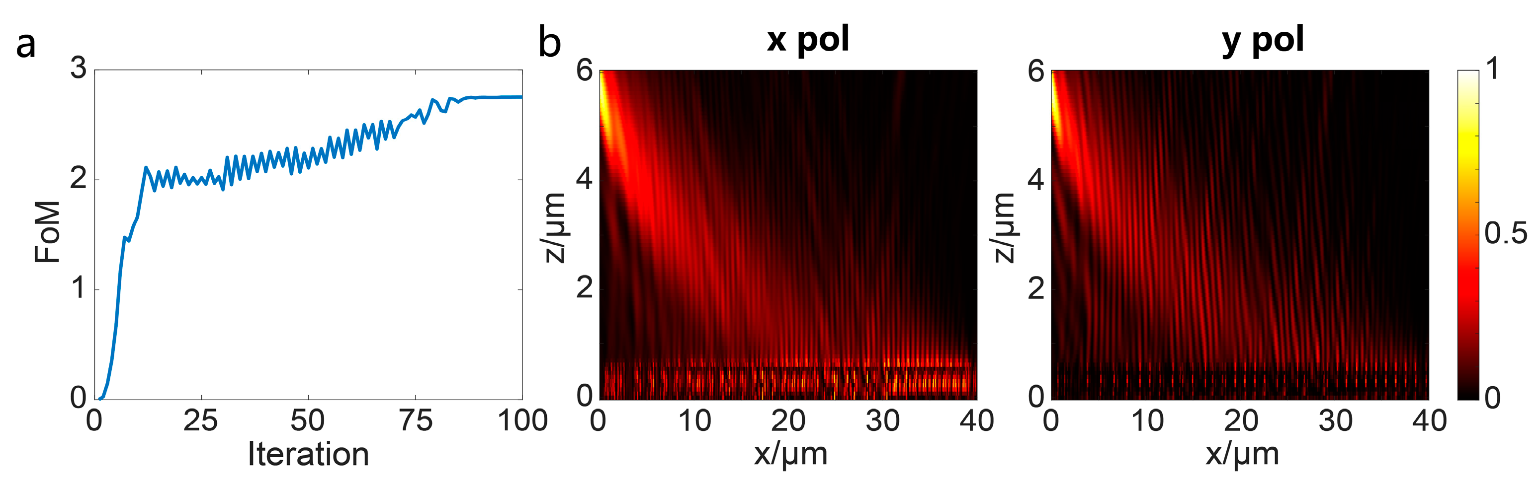
2.2. Large-Scale Design
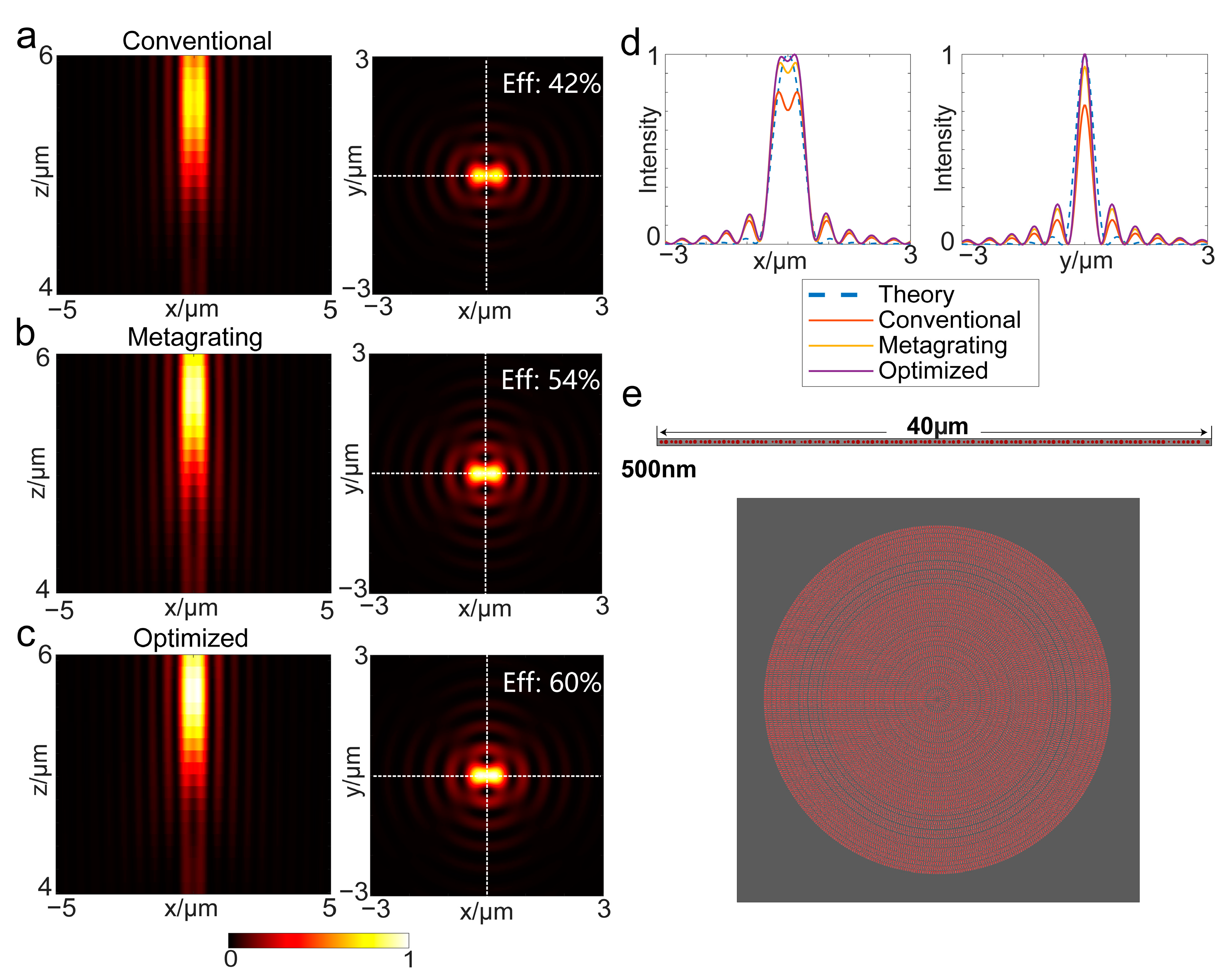
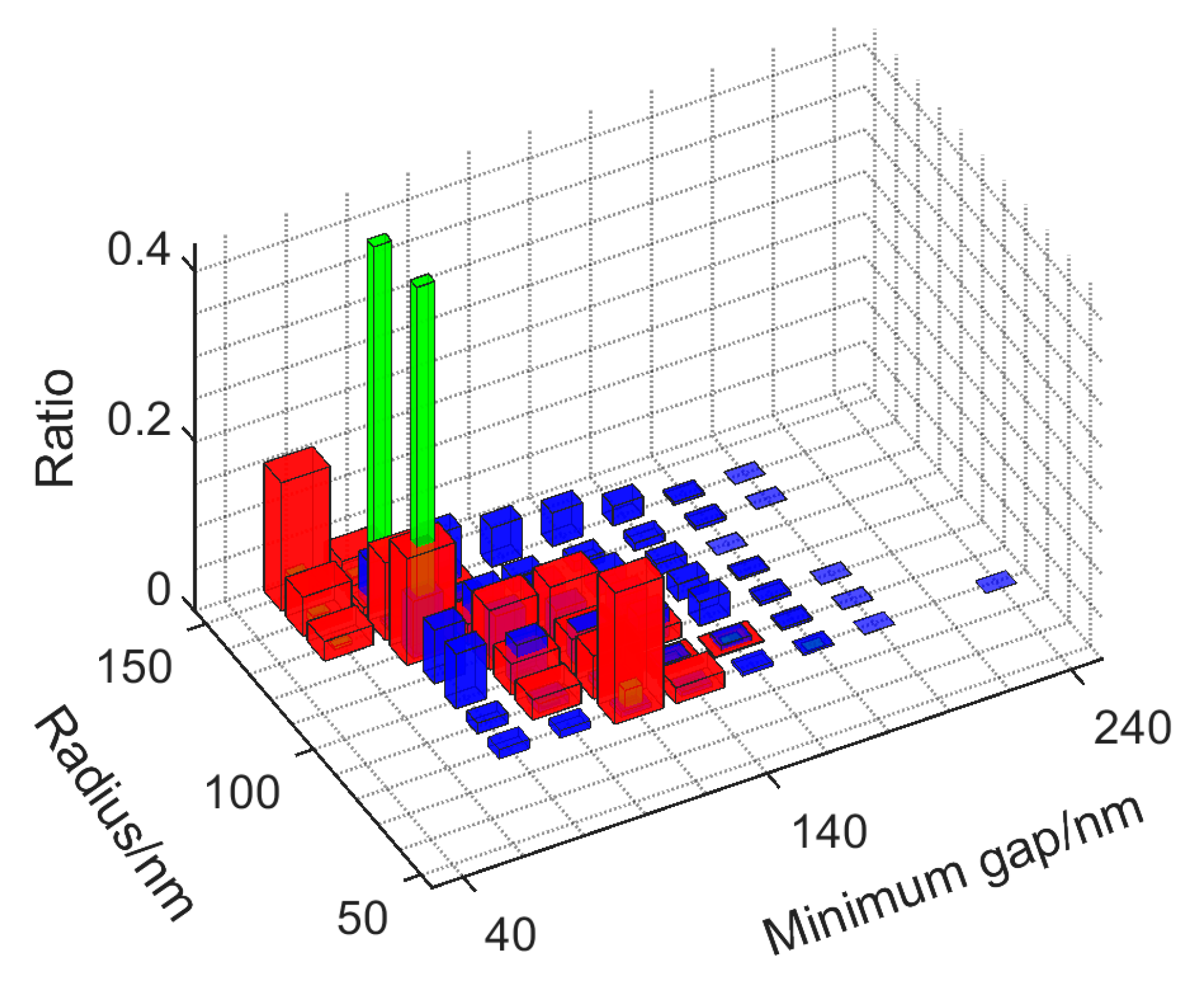
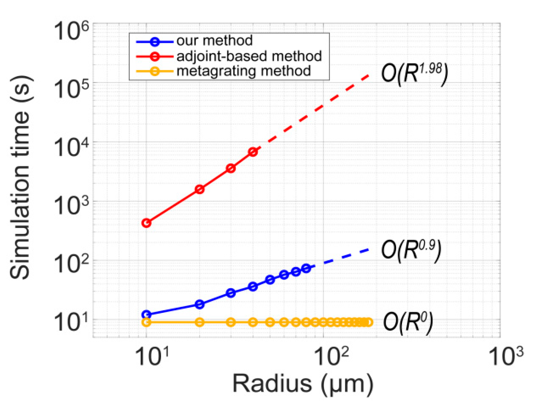
Since a metalens is nearly symmetrical about its center, we can focus on optimizing the design in the radial direction and then use symmetry to construct a complete metalens. To facilitate the design of the large-scale metalens, the process is divided into two parts.
The first step involves designing a one-dimensional arrangement of structures by the adjoint-based level-set optimization method, as illustrated in Figure 2a. Here, the outgoing wavefront adheres to a radial phase distribution, such as the hyperbolic phase:
φ ( R ) = 2 π λ R 2 + f 2 f ,
where R is the radial position of the metalens, f is the focal length, and λ is the operation wavelength. This approach differs from the general adjoint-based method, which typically optimizes the topology of pillars [21,37]. In this design, only the shape is modified without altering the topology in order to minimize errors caused by structural deformation in the second step. This ensures greater consistency and reduces potential fabrication issues during scaling.
The second step is to extend the design from a one-dimensional structure to a two-dimensional structure, as illustrated in Figure 2b. The entire metalens is divided into multiple concentric rings, based on the radial position of the pillars in the one-dimensional structure. Each ring is filled with corresponding pillars, arranged in a rotating pattern. Because the gaps between adjacent pillars remain the same while the perimeters of the rings vary, the number of pillars in each ring gradually increases as you move radially outward. This method leverages the central symmetry of the metalens to simplify the design process. However, unlike the traditional adjoint-based method, this approach does not strictly adhere to the simulation results during optimization. Since the arrangement in the one-dimensional structure and that in the two-dimensional structure are not identical, there may be some changes in the response of the pillars and the output wavefront. Nevertheless, by ensuring the pillars remain isolated in the design, the impact of structural deformation during the transition to a two-dimensional metalens is minimized. Additionally, arranging the pillars in rings helps preserve some characteristics of the one-dimensional design. The feasibility of this method is demonstrated through simulations in the following sections.

3. Results

To demonstrate the effectiveness of the adjoint-based level-set optimization method, as well as the large-scale metalenses design strategy, we designed a metalens with an NA of 0.99, operating at a wavelength of 1050 nm. The diameter of the metalens is 80 μm, resulting in a focal length of 5.7 μm. The metalens consists of silicon pillars with a height of 500 nm on the silica substrate, making it compatible with standard semiconductor manufacturing processes. The refractive index of silicon is 3.55, and that of the silica is 1.45. Circular pillars were used as the basic elements to illustrate the level-set method. The output plane was positioned 300 nm above the surface of the structure. The desired electric fields for both the x-polarized source and y-polarized source were defined as follows:
x   pol :   E x d = n exp ( j φ ( R ) ) cos θ E y d = 0 E z d = n exp ( j φ ( R ) ) sin θ cos θ ,
y   pol :   E x d = 0 E y d = n cos θ exp ( j φ ( R ) ) E z d = 0 ,
where n is the background index, and θ = arctan ( R / f ) is the local output angle of the metalens.
To ensure that the design is polarization-insensitive, the gradients of the parameters were calculated separately for x-polarized and y-polarized light incidences. These gradients were then combined using a weighted average. By adjusting the weights, we balanced the optimization process for both polarizations, ensuring that the metalens performs in a balanced way under varying polarization conditions.
F o M p = w x p o l F o M x p o l p + w y p o l F o M y p o l p ,
where w x p o l and w y p o l are the coefficients of the gradients under different polarizations.
The initial structure consisted of 120 circular pillars, each with a radius of 110 nm, spaced 350 nm apart in the x-direction. All pillars were aligned along the x-axis, with a period of 500 nm in the y-direction, and the total length in the x-direction was 40 μm. The level-set function for each pillar in Cartesian coordinates was defined as follows:
ϕ ( x , y ) = ( x x 0 ) 2 + y 2 r 0 2 ,
where x0 is the center position of the circular pillar, and r0 is the radius of the circular pillar, as shown in Figure 2a.
We optimized both the x-coordinate and the radius of each pillar with a precision of 1 nm, resulting in a total of 240 independent variables. This level of precision in parameter adjustments can be achieved through the electro-beam lithography fabrication process. To account for fabrication constraints, we set a minimum gap of 80 nm between adjacent pillars and a minimum pillar radius of 80 nm. These constraints ensured that the design remained feasible for practical manufacturing processes, while maintaining the desired performance.
The design ran for 100 iterations. The FoM increased rapidly during the first ten iterations and then oscillated, eventually reaching a plateau after 85 iterations, as shown in Figure 3a. The intensity distributions in the xz plane of the optimized one-dimensional design under the x-polarized and y-polarized plane source were simulated using Ansys FDTD and are displayed in Figure 3b, showing clear focusing phenomena.
Then, this one-dimensional structure was extended to a two-dimensional metalens (Figure 4e). For ease of comparison, the conventional metalens was designed using the phase-mapping approach, consisting of 500 nm tall circular Si pillar meta-atoms, arranged on a rectangular lattice with a period of 350 nm. The minimum radius of the pillars was set to 80 nm. The phase and transmittance of the pillars with varying radii are shown in Appendix A. Additionally, we simulated a metalens designed using the metagrating method [23], consisting of 500 nm tall circular Si pillar meta-atoms, applying the same fabrication constraints: a minimum gap of 80 nm between adjacent pillars and a minimum radius of 80 nm. Further details on this design can be found in Appendix B.
The focusing performances of these metalenses were simulated using Ansys FDTD, with PML applied to all boundaries and an x-polarized plane wave source. Additionally, we calculated the theoretical focal-spot intensity for a lens with NA = 0.99 using the Richards–Wolf vector diffraction integration method [38]. The intensity distributions of the focal spots are compared in Figure 4. The simulation results indicated that the focusing efficiency of our optimized metalens was 60%, while the conventional metalens achieved 42%, and the metagrating-design metalens reached 54%. The electric field distributions 300 nm above the metalenses are shown in Appendix C.
Using a linearly polarized input source, the high-NA metalens produces a significantly elliptical focal spot in simulation, primarily due to the enhancement of the Iz component [23,39]. As shown in Appendix D Figure A5, when a linearly polarization plane wave is incident on a lens with a large numerical aperture, a strong longitudinal polarization component will be generated at the focus point. This causes the focal spot to stretch along the polarization direction of the incident light. In our simulations, x-polarized light was used, elongated into a strip along the x-direction. When the high-NA metalens has varying polarization responses or insufficient focusing capability, the proportion of the Iz component increases, and the focal spot may even split, resembling the intensity distribution of the Iz component. Comparing the focal spots of different designs, we see that our optimized metalens showed the smallest decrease in intensity at the center of the focal spot, indicating that the shape of the focal spot could also be improved through optimization (see Appendix D for more details).
Despite the strict fabrication constraints, optimization methods still yielded designs with a higher focusing efficiency. We compiled the radii of the pillars and the minimum intervals between adjacent pillars. Comparing the number distribution of pillars with different combinations of radii and minimum intervals, as shown in Figure 5, we observed that our optimized metalens tends to have larger radii and larger gaps. Unlike the conventional design, which follows a fixed lattice arrangement [22], our method—free from lattice constraints—better utilized the available fabrication parameters to optimize the design.

4. Discussion

We compared the simulation time per optimization epoch across different methods, as the simulation cost accounts for the majority of the overall optimization cost. We tested the simulation time of metalenses with different radii, R, on a server equipped with two 56-cores processors, whose model is Intel Xeon Platinum 8176, produced by Intel, California, America. We used the computational complexity, O ( R n ) , to evaluate the simulation time of different methods, indicating that the simulation time is a linear function of the metalens radius, R, raised to the nth power. The simulation time for the conventional adjoint-based method, which requires simulating the whole metalens, scaled approximately O ( R 1.98 ) , while the simulation time of our method scaled approximately O ( R 0.9 ) , as shown in Figure 6. This demonstrates that our method significantly reduces computation cost in the large-scale design. Although the simulation time for the metagrating method [23] only depends on the number of metagrating designs used, this method often needs additional fine-tuning of each structure in different regions to achieve higher efficiency, making it more complicated than our overall design process.
This design method, which extends from a one-dimensional structure to a two-dimensional metalens, may introduce new non-local errors. However, our optimized metalens still shows significant improvement compared to the conventional metalens. Additionally, because the optimization covers only a radial array, it reduces the computational cost compared to previous optimization methods [18,22,23].
Although our optimized metalens demonstrates significant improvement compared to conventional designs, extending from a one-dimensional structure to a two-dimensional metalens will introduce new non-local errors. To further improve the focusing equality, a neural network can be used to fine-tune our optimized metalenses. Here, this network has learned the mutual coupling effects [17]. In addition, increasing the number of polynomial terms of the level-set function, which can improve the diversity of structural shapes [35], also contributes to an improved metalens performance.

5. Conclusions

We propose a new design strategy for large-scale metalenses combining the adjoint-based method with the level-set method, which extends the one-dimensional metalens designs to two-dimensional metalenses. This approach further reduces the simulation area, making the relationship between the computational cost and the metalens diameter closer to linear, significantly cutting the computational cost for large-scale designs. Our optimized metalens shows significant improvements in the focusing efficiency compared to conventional designs, notably from 42% to 60% at NA = 0.99, and the deformation of the focal spot caused by the polarization response differences under a linearly polarized source is also improved. Compared with the recent metalens designed by the supercell method in NIR (900 nm) with an NA of 0.8 [26], whose focusing efficiency is 66%, our design has close focusing efficiency, with a significantly higher NA. This method can easily be applied to metalens designs with larger radii in practical applications. Furthermore, this approach can be extended to other devices with central symmetry.

Author Contributions

H.L. and J.L. conceived the idea of the paper; Y.Z. performed the calculations; Y.Z., Y.L., H.L. and J.L. wrote the manuscript. All authors contributed to the analysis of the results. All authors have read and agreed to the published version of the manuscript.

Funding

This work was funded by the National Key R&D Program of China (Grants 2022YFA1404304) and National Natural Science Foundation of China (Grant Nos. 12374363, 12074444, and 11704421). H.L. acknowledges the “GDTZ” plan support under contract No. 2021TQ06X161 and Fundamental Research Funds for the Central Universities, Sun Yat-sen University, under contract No. 241gqb016.

Institutional Review Board Statement

Not applicable.

Informed Consent Statement

Not applicable.

Data Availability Statement

The data are contained within the article.

Conflicts of Interest

The authors declare no conflicts of interest.

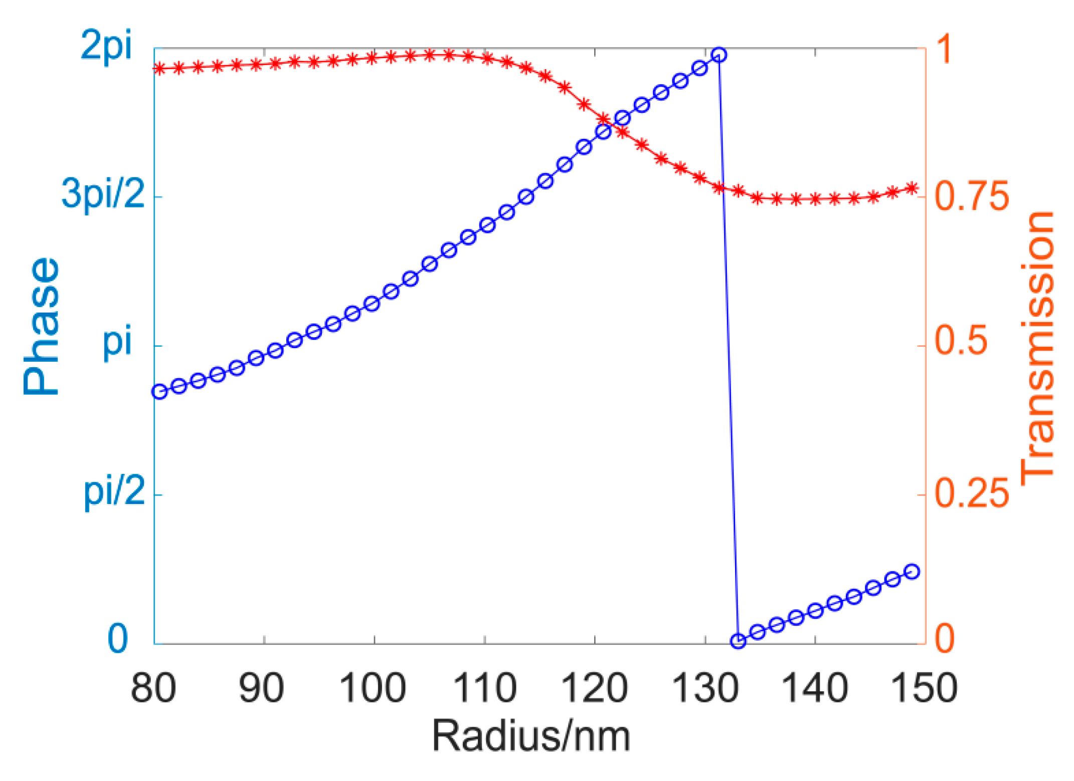
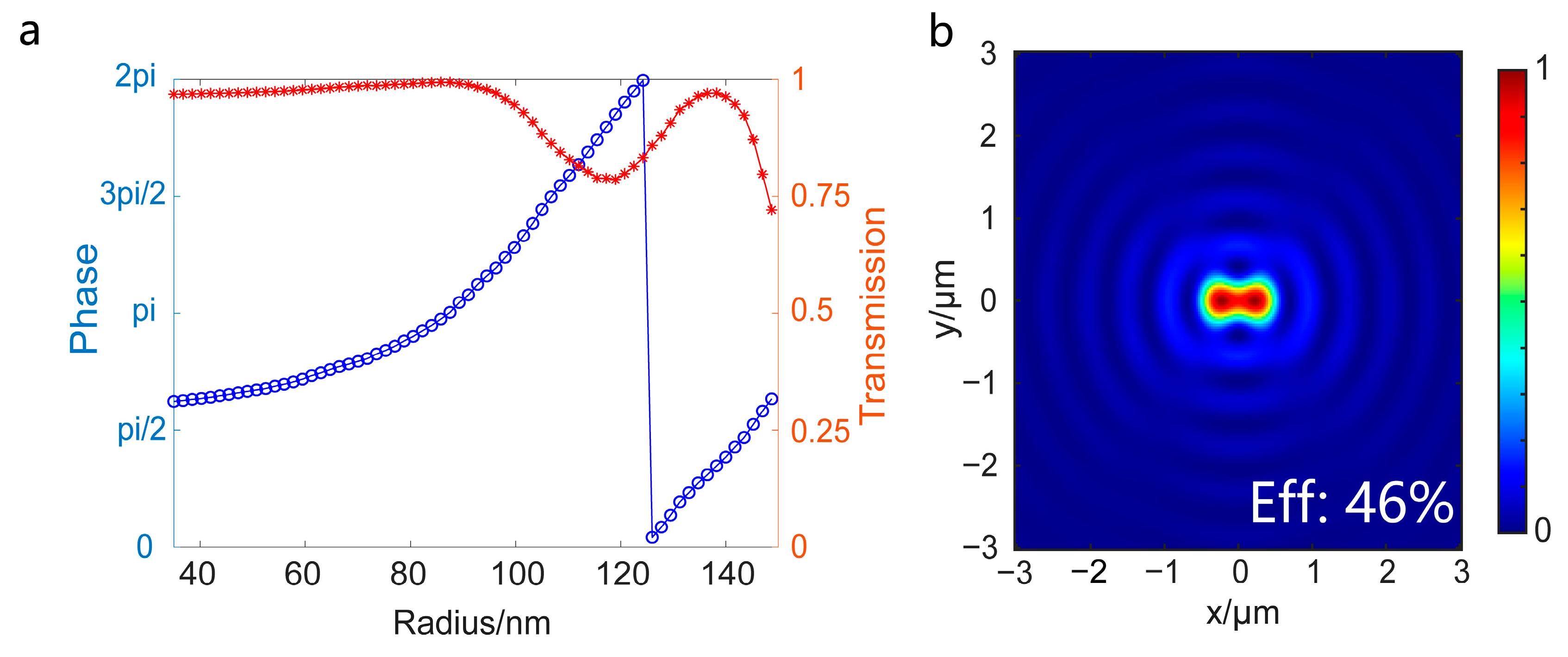
Appendix A. The Design of the Metalens Using the Phase Mapping Method

We performed FDTD simulations to determine the phase and transmission of different meta-atoms. The size of the unit cell is 350 nm, and the height of the meta-atoms is the 500 nm. We performed a parameter sweep of the radius in 2 nm steps, and the radius ranges from 80 nm to 148 nm under the strict fabrication constraints. The phase control range is 1.4π, and the lowest transmittance of the pillars is above 75%, as shown in Figure A1.
Figure A1. The phase and transmission of the periodic circular pillars with different radii used in the conventional metalens. The dots represent the results of the parameter sweep of the radius in 2 nm steps. The red dots correspond to the transmission of pillars and the blue dots correspond to the phase of pillars.
Photonics 11 00940 g0a1
To achieve a full 2π phase shift and compare the impact of different phase coverage ranges, we simulated an additional metalens using 600 nm high Si pillars, while maintaining a unit cell size of 350 nm. As a result, the lowest transmittance of the pillars was approximately 75%, and the efficiency of the metalens constructed with these meta-atoms was 46%, as shown in Figure A2. It is important to note that, in order to cover the full 2π phase range, we had to relax the fabrication constraints, allowing the pillars’ radius to range from 35 nm to 150 nm. However, the focusing efficiency of this metalens was still lower than that of our optimized metalens.
Figure A2. (a) The phase and transmission of the periodic circular pillars with different radii and whose phase range covers 2π. The dots represent the results of the parameter sweep of the radius in 2nm steps. The red dots correspond to the transmission of pillars and the blue dots correspond to the phase of pillars. (b) The focal spot of the metalens with 2π phase range simulated in FDTD. The number at the bottom right corner is the focusing efficiency.
Photonics 11 00940 g0a2

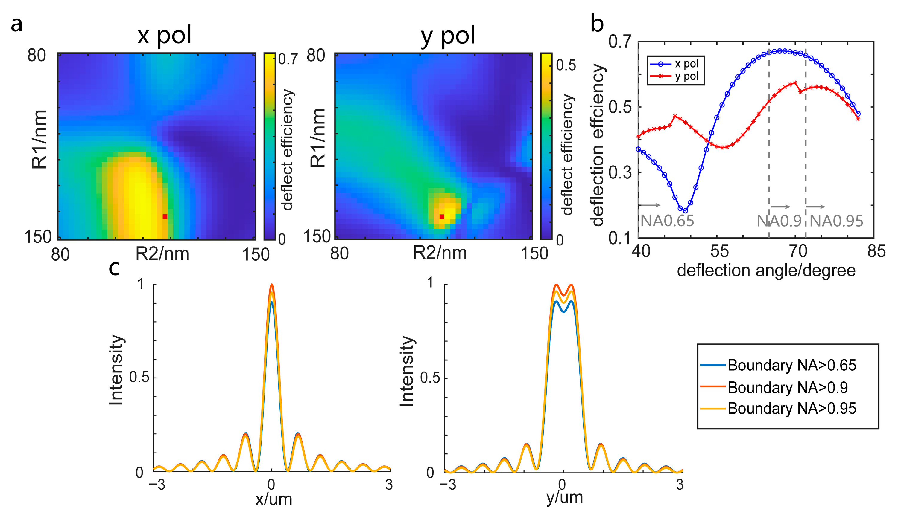
Appendix B. The Design of the Metalens Using the Metagrating Method

In this design, we used a dimer, consisting of two circular Si pillars, for the metagrating structure. We optimized the radius of the dimer, the interval between the pillars, and the y-direction period. The dimer was selected to achieve the highest and most balanced deflection efficiency under x-polarized and y-polarized sources, at a deflection angle of 80°. During the optimization process, the height of the pillars is fixed at 500 nm, the minimum interval between the pillars is 80 nm, and the radius ranges from 80 nm to 150 nm. The optimized radii of the pillars are 142 nm and 118 nm, with an interval of 80 nm and a y-direction period of 460 nm, as shown in Appendix B Figure A3a.
When the deflection angle was reduced to 70°, we adjusted the y-direction period to 410 nm to maintain better deflection efficiency. However, due to parameter limitations, the deflection efficiencies remained suboptimal, and the efficiency differences between different polarizations became more pronounced at deflection angles smaller than 80°, as shown in Figure A3b.
The metalens was composed of two regions. The central area, within the boundary of the NA, was designed using the phase-mapping method, while the remaining area was arranged using the metagrating method. We designed three metalenses with different boundaries between the phase-mapping region and the metagrating region. For the design with an NA boundary of 0.9, the focusing efficiency reached 54%, which was the maximum of the three designs, as shown in Figure A3c. This value was higher than the focusing efficiency of the conventional metalens with phase-mapping method but lower than that of our optimized metalens.
Figure A3. Simulation results of the metagrating and three metalenses with different boundaries between the phase-mapping region and the metagrating region. (a) The deflection efficiency distribution as a function of the dimer radii under the x-polarized and y-polarized sources at a deflection angle of 80°, with a y-period of 460 nm. The red square indicates the dimer radii used in the design. (b) The deflection efficiency as a function of different deflection angles. The y-period is 460 nm for deflection angles above 70° and is reduced to 410 nm for angles below 70°. The three gray dashed lines point out the boundaries between the phase-mapping region and the metagrating region of the three metalenses with NA values of 0.65, 0.9, and 0.95. (c) The intensity distributions in the x-direction and y-direction of the focal spots for the three metalenses with different boundaries.
Photonics 11 00940 g0a3

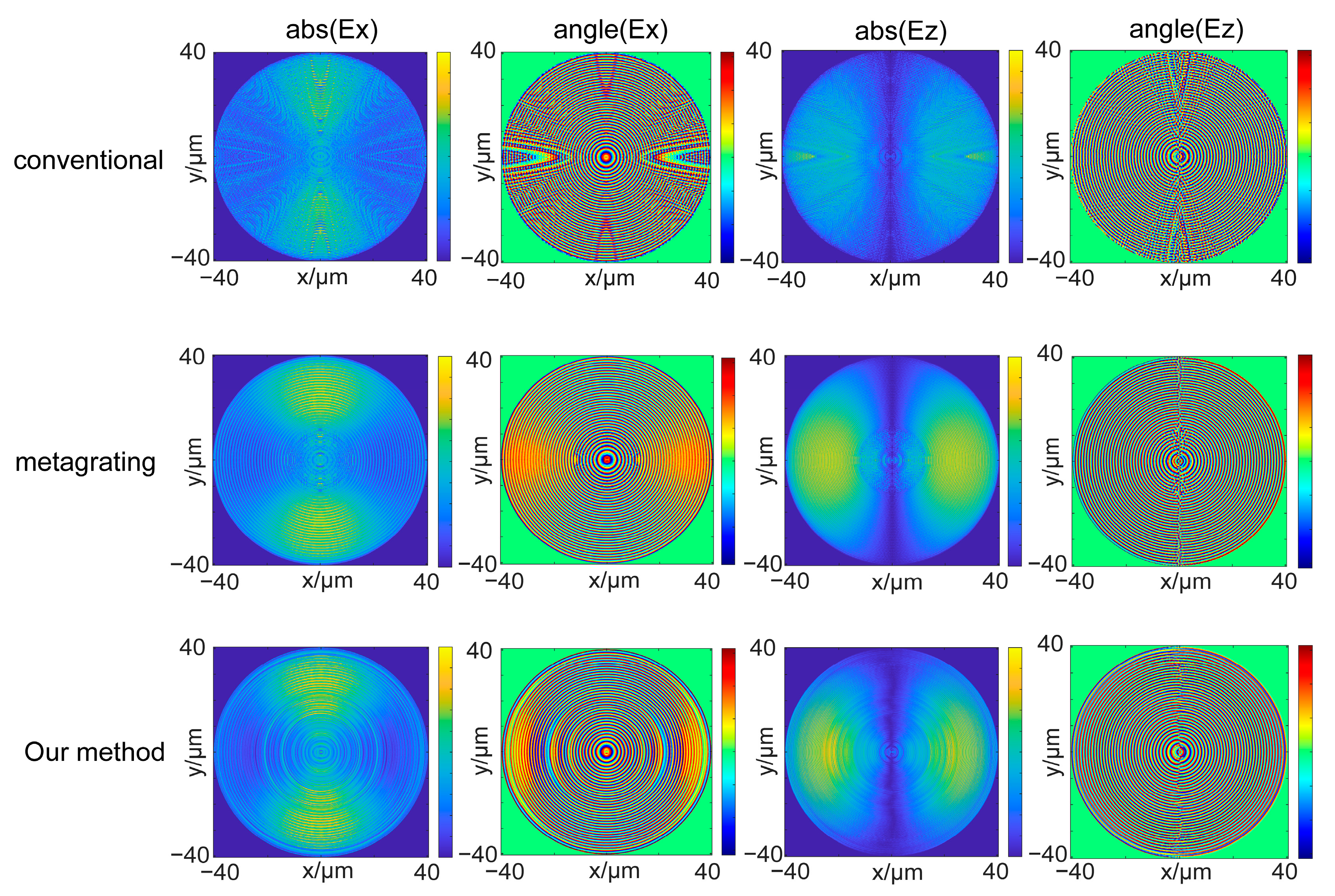
Appendix C. The Field Distribution in the Metalenses

We simulated the fields 300 nm above the conventional metalens, the metagrating-design metalens, and our optimized metalens under an x-polarized plane source. The modulus of the field components clearly showed the polarization transformation effect in high-NA metalenses, as shown in Figure A4. The Ex phase distribution of our optimized metalens exhibited noticeable nonuniformity, indicating that the metalens did not have a uniform deflection effect. This nonuniformity could affect the focusing efficiency and distort the shape of the focal spot. In the field distribution of the conventional metalens, patterns caused by sampling the rectangular lattice on the folded phase were evident. In contrast, the field distribution of our optimized metalens was not impacted by these lattice sampling patterns, resulting in a more uniform field distribution and potentially better performance.
Figure A4. The Ex and Ez component of the field distributions on the 300 nm above the metalenses.
Photonics 11 00940 g0a4

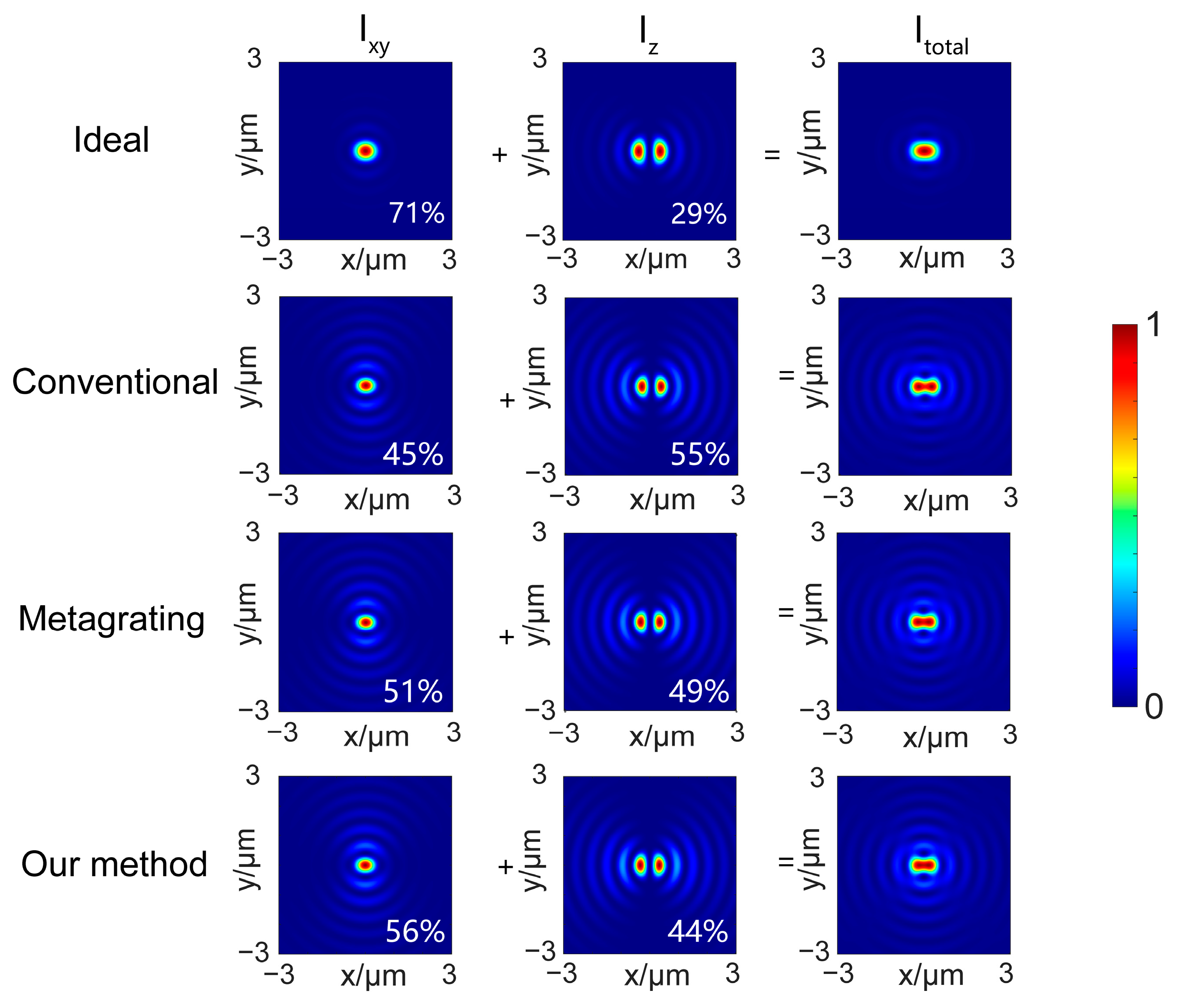
Appendix D. The Iz and Ixy Components of the Focal Spot

We noticed that the focal spot of the simulated metalenses deviates from the ideal airy pattern, with distortion in the high-NA lens caused by the depolarization effect. To better characterize the focal spot, we calculated the focal spot of an ideal lens with NA = 0.99 under an x-polarized linearly incident beam using the Richards–Wolf vector diffraction integration method in MATLAB R2020a, as shown in Figure A5. The focal spot of the ideal lens was obviously flatter than the FDTD results of the conventional metalens, the metalens designed by metagrating-design method, and our optimized metalens. By analyzing the energy distribution of different components, we found that the higher the amount of energy that the Iz component occupies, the more severe the deformation. In the idea lens, the Iz component occupied 29% of the energy of the focal spot energy. Meanwhile, in the conventional metalens, it occupied 55%, leading to obvious deformation of the focal spot. By contrast, our optimization method reduced the energy proportion of the Iz component to 44%, resulting in less deformation. Although the metagrating-design method could also reduce the Iz component to 49%, it was still not as good as our method.
Figure A5. Simulated focusing performance of metalenses by an x-polarized linearly incident beam. From left to right: the Ixy component of focal spot, the Iz component of focal spot, and the intensity of focal spot. The numbers in the bottom right corner represent the energy proportions of the corresponding components.
Photonics 11 00940 g0a5

References

  1. Khorasaninejad, M.; Chen, W.T.; Devlin, R.C.; Oh, J.; Zhu, A.Y.; Capasso, F. Metalenses at visible wavelengths: Diffraction-limited focusing and subwavelength resolution imaging. Science 2016, 352, 1190–1194. [Google Scholar] [CrossRef] [PubMed]
  2. Wang, S.; Wu, P.C.; Su, V.; Lai, Y.; Chen, M.; Kuo, H.Y.; Chen, B.H.; Chen, Y.H.; Huang, T.; Wang, J.; et al. A broadband achromatic metalens in the visible. Nat. Nanotechnol. 2018, 13, 227–232. [Google Scholar] [CrossRef] [PubMed]
  3. Chen, J.; Ye, X.; Gao, S.; Chen, Y.; Zhao, Y.; Huang, C.; Qiu, K.; Zhu, S.; Li, T. Planar wide-angle-imaging camera enabled by metalens array. Optica 2022, 9, 431–437. [Google Scholar] [CrossRef]
  4. Juodėnas, M.; Strandberg, E.; Grabowski, A.; Gustavsson, J.; Šípová-Jungová, H.; Larsson, A.; Käll, M. High-angle deflection of metagrating-integrated laser emission for high-contrast microscopy. Light Sci. Appl. 2023, 12, 251. [Google Scholar] [CrossRef] [PubMed]
  5. Chen, W.T.; Park, J.; Marchioni, J.; Millay, S.; Yousef, K.M.A.; Capasso, F. Dispersion-engineered metasurfaces reaching broadband 90% relative diffraction efficiency. Nat. Commun. 2023, 14, 2544. [Google Scholar] [CrossRef]
  6. Yin, Y.; Jiang, Q.; Wang, H.; Liu, J.; Xie, Y.; Wang, Q.; Wang, Y.; Huang, L. Multi-Dimensional Multiplexed Metasurface Holography by Inverse Design. Adv. Mater. 2024, 36, 2312303. [Google Scholar] [CrossRef]
  7. He, G.; Zheng, Y.; Zhou, C.; Li, S.; Shi, Z.; Deng, Y.; Zhou, Z. Multiplexed manipulation of orbital angular momentum and wavelength in metasurfaces based on arbitrary complex-amplitude control. Light Sci. Appl. 2024, 13, 98. [Google Scholar] [CrossRef]
  8. Kim, G.; Kim, Y.; Yun, J.; Moon, S.; Kim, S.; Kim, J.; Park, J.; Badloe, T.; Kim, I.; Rho, J. Metasurface-driven full-space structured light for three-dimensional imaging. Nat. Commun. 2022, 13, 5920. [Google Scholar] [CrossRef]
  9. Zou, X.; Zhang, Y.; Lin, R.; Gong, G.; Wang, S.; Zhu, S.; Wang, Z. Pixel-level Bayer-type colour router based on metasurfaces. Nat. Commun. 2022, 13, 3288. [Google Scholar] [CrossRef]
  10. Zhang, X.G.; Sun, Y.L.; Zhu, B.; Jiang, W.X.; Yu, Q.; Tian, H.W.; Qiu, C.; Zhang, Z.; Cui, T.J. A metasurface-based light-to-microwave transmitter for hybrid wireless communications. Light Sci. Appl. 2022, 11, 126. [Google Scholar] [CrossRef]
  11. Liu, Z.; Guo, T.; Tan, Q.; Hu, Z.; Sun, Y.; Fan, H.; Zhang, Z.; Jin, Y.; He, S. Phase Interrogation Sensor Based on All-Dielectric BIC Metasurface. Nano Lett. 2023, 23, 10441–10448. [Google Scholar] [CrossRef] [PubMed]
  12. Zaidi, A.; Rubin, N.A.; Meretska, M.L.; Li, L.W.; Dorrah, A.H.; Park, J.; Capasso, F. Metasurface-enabled single-shot and complete Mueller matrix imaging. Nat. Photonics 2024, 18, 704–712. [Google Scholar] [CrossRef]
  13. Zheng, Z.; Smirnova, D.; Sanderson, G.; Cuifeng, Y.; Koutsogeorgis, D.C.; Huang, L.; Liu, Z.; Oulton, R.; Yousefi, A.; Miroshnichenko, A.E.; et al. Broadband infrared imaging governed by guided-mode resonance in dielectric metasurfaces. Light Sci. Appl. 2024, 13, 249. [Google Scholar] [CrossRef] [PubMed]
  14. Lin, X.; Rivenson, Y.; Yardimci, N.T.; Veli, M.; Luo, Y.; Jarrahi, M.; Ozcan, A. All-optical machine learning using diffractive deep neural networks. Science 2018, 361, 1004–1008. [Google Scholar] [CrossRef]
  15. Luo, X.; Hu, Y.; Ou, X.; Li, X.; Lai, J.; Liu, N.; Cheng, X.; Pan, A.; Duan, H. Metasurface-enabled on-chip multiplexed diffractive neural networks in the visible. Light Sci. Appl. 2022, 11, 158. [Google Scholar] [CrossRef]
  16. Liang, H.; Martins, A.; Borges, B.V.; Zhou, J.; Martins, E.R.; Li, J.; Krauss, T.F. High performance metalenses: Numerical aperture, aberrations, chromaticity, and trade-offs. Optica 2019, 6, 1461–1470. [Google Scholar] [CrossRef]
  17. An, S.; Zheng, B.; Shalaginov, M.Y.; Tang, H.; Li, H.; Zhou, L.; Dong, Y.; Haerinia, M.; Agarwal, A.M.; Rivero-Baleine, C.; et al. Deep Convolutional Neural Networks to Predict Mutual Coupling Effects in Metasurfaces. Adv. Opt. Mater. 2022, 10, 2102113. [Google Scholar] [CrossRef]
  18. Cai, H.; Srinivasan, S.; Czaplewski, D.A.; Martinson, A.B.F.; Gosztola, D.J.; Stan, L.; Loeffler, T.; Sankaranarayanan, S.K.R.S.; López, D. Inverse design of metasurfaces with non-local interactions. NPJ Comput. Mater. 2020, 6, 116. [Google Scholar] [CrossRef]
  19. Liang, H.; Lin, Q.; Xie, X.; Sun, Q.; Wang, Y.; Zhou, L.; Liu, L.; Yu, X.; Zhou, J.; Krauss, T.F.; et al. Ultrahigh Numerical Aperture Metalens at Visible Wavelengths. Nano Lett. 2018, 18, 4460–4466. [Google Scholar] [CrossRef]
  20. Miller, O.D. Photonic Design: From Fundamental Solar Cell Physics to Computational Inverse Design. Ph.D. Thesis, UC Berkeley, Berkeley, CA, USA, 2012. [Google Scholar]
  21. Chung, H.; Miller, O.D. High-NA achromatic metalenses by inverse design. Opt. Express 2020, 28, 6945–6965. [Google Scholar] [CrossRef]
  22. Mansouree, M.; McClung, A.; Samudrala, S.; Arbabi, A. Large-Scale Parametrized Metasurface Design Using Adjoint Optimization. ACS Photonics 2021, 8, 455–463. [Google Scholar] [CrossRef]
  23. Zhang, J.; Liang, H.; Long, Y.; Zhou, Y.; Sun, Q.; Wu, Q.; Fu, X.; Martins, E.R.; Krauss, T.F.; Li, J.; et al. Metalenses with Polarization-Insensitive Adaptive Nano-Antennas. Laser Photon. Rev. 2022, 16, 2200268. [Google Scholar] [CrossRef]
  24. Phan, T.; Sell, D.; Wang, E.W.; Doshay, S.; Edee, K.; Yang, J.; Fan, J.A. High-efficiency, large-area, topology-optimized metasurfaces. Light Sci. Appl. 2019, 8, 48. [Google Scholar] [CrossRef] [PubMed]
  25. Zhou, Y.; Mao, C.; Gershnabel, E.; Chen, M.; Fan, J.A. Large-Area, High-Numerical-Aperture, Freeform Metasurfaces. Laser Photon. Rev. 2024, 18, 2300988. [Google Scholar] [CrossRef]
  26. Paniagua-Domínguez, R.; Yu, Y.F.; Khaidarov, E.; Choi, S.; Leong, V.; Bakker, R.M.; Liang, X.; Fu, Y.H.; Valuckas, V.; Krivitsky, L.A.; et al. A Metalens with a Near-Unity Numerical Aperture. Nano Lett 2018, 18, 2124–2132. [Google Scholar] [CrossRef]
  27. Caselles, V.; Catté, F.; Coll, T.; Dibos, F. A geometric model for active contours in image processing. Numer. Math. 1993, 66, 1–31. [Google Scholar] [CrossRef]
  28. Santosa, F. A level-set approach for inverse problems involving obstacles. ESAIM COCV 1996, 1, 17–33. [Google Scholar] [CrossRef]
  29. Lalau-Keraly, C.M.; Bhargava, S.; Miller, O.D.; Yablonovitch, E. Adjoint shape optimization applied to electromagnetic design. Opt. Express 2013, 21, 21693–21701. [Google Scholar] [CrossRef]
  30. Mansouree, M.; Arbabi, A. Metasurface Design Using Level-Set and Gradient Descent Optimization Techniques. In Proceedings of the 2019 International Applied Computational Electromagnetics Society Symposium (ACES), Nanjing, China, 8–12 August 2019. [Google Scholar]
  31. Dong, L.; Kong, W.; Wang, C.; Pu, M.; Liu, X.; Luo, Y.; Luo, X. Quasi-continuous metasurface for high-efficiency beam deflection based on multi-objective level-set optimization. Opt. Mater. Express 2022, 12, 3667–3678. [Google Scholar] [CrossRef]
  32. Bao, H.; Zhang, F.; Pu, M.; He, Q.; Xu, M.; Guo, Y.; Li, L.; Ma, X.; Li, X.; Luo, X. Field-Driven Inverse Design of High-Performance Polarization-Multiplexed Meta-devices. Laser Photon. Rev. 2024, 18, 2301158. [Google Scholar] [CrossRef]
  33. Shen, Y.; Wong, N.; Lam, E.Y. Level-set-based inverse lithography for photomask synthesis. Opt. Express 2009, 17, 23690–23701. [Google Scholar] [CrossRef] [PubMed]
  34. Saad-Falcon, A.; Howard, C.; Romberg, J.; Allen, K. Level set methods for gradient-free optimization of metasurface arrays. Sci. Rep. 2024, 14, 16674. [Google Scholar] [CrossRef] [PubMed]
  35. Dainese, P.; Marra, L.; Cassara, D.; Portes, A.; Oh, J.; Yang, J.; Palmieri, A.; Rodrigues, J.R.; Dorrah, A.H.; Capasso, F. Shape optimization for high efficiency metasurfaces: Theory and implementation. arXiv 2024, arXiv:2405.03930. [Google Scholar]
  36. Bertsekas, D.P. Constrained Optimization and Lagrange Multiplier Methods; Academic Press: Cambridge, MA, USA, 1982. [Google Scholar]
  37. Sell, D.; Yang, J.; Doshay, S.; Yang, R.; Fan, J.A. Large-Angle, Multifunctional Metagratings Based on Freeform Multimode Geometries. Nano Lett. 2017, 17, 3752–3757. [Google Scholar] [CrossRef] [PubMed]
  38. Richards, B.; Wolf, E.; Gabor, D. Electromagnetic diffraction in optical systems, II. Structure of the image field in an aplanatic system. Proc. R. Soc. Lond. Ser. A 1959, 253, 358–379. [Google Scholar]
  39. Gao, J.; Yan, S.; Zhou, Y.; Liang, G.; Zhang, Z.; Wen, Z.; Chen, G. Polarization-conversion microscopy for imaging the vectorial polarization distribution in focused light. Optica 2021, 8, 984–994. [Google Scholar] [CrossRef]
Figure 1. Flow diagram showing steps in the adjoint-based method with level-set method.
Photonics 11 00940 g001
Figure 2. Illustration of the large-scale metalens design method. (a) Design process of the one-dimensional structure. (b) Arrangement of the two-dimensional metalens created from the one-dimensional structure. The blue dots show the arrangement of one-dimension structure.
Photonics 11 00940 g002
Figure 3. Design process and simulations of the one-dimensional metalens. (a) The FoM of the optimized metalens during the optimization process. (b) The intensity distribution on the xz plane of the optimized metalens under x-polarized plane source or y-polarized plane source.
Photonics 11 00940 g003
Figure 4. Simulations of the conventional metalens, the metagrating-design metalens, and our optimized metalens. The intensity distributions on the xz plane near the focal spots and xy plane on the focal plane of (a) the conventional metalens, (b) the metagrating-design metalens, and (c) our optimized metalens. The focusing efficiency of our optimized metalens is 60%, while the focusing efficiency of the conventional metalens is 42% and that of metagrating-design metalens is 54%. (ac) Normalized with the same maximum intensity. (d) The intensity distributions in x-direction and y-direction. The white dotted lines in (ac) point out the direction of the intensity distributions in (d). (e) Illustration of the one-dimensional optimized metalens and the final two-dimensional optimized metalens.
Photonics 11 00940 g004
Figure 5. The number distribution of pillars with different combinations of radii and minimum gaps between adjacent pillars. The red column is the distribution of the conventional metalens, the green column is the distribution of the metalens designed by metagrating method, and the blue column is the distribution of our optimized metalens.
Photonics 11 00940 g005
Figure 6. The simulation time for each optimization epoch of three methods.
Photonics 11 00940 g006
Disclaimer/Publisher’s Note: The statements, opinions and data contained in all publications are solely those of the individual author(s) and contributor(s) and not of MDPI and/or the editor(s). MDPI and/or the editor(s) disclaim responsibility for any injury to people or property resulting from any ideas, methods, instructions or products referred to in the content.

