Abstract
In this study, the effects of variations in the height () and bottom radius () of black silicon microstructures on their absorptance and photoelectric response efficiency were analyzed. By using the relation to combine the parameters, it was found that changes in morphology affected the absorptance of black silicon microstructures, with being directly proportional to the absorptance, while was inversely proportional. A positive correlation was observed between and absorptance. However, the correlation between and photoelectric response efficiency was not significant. Through Raman spectroscopy analysis of the samples, it was concluded that as the laser ablation energy density increased, more lattice defects were introduced, weakening the charge carrier transport efficiency. This study further elucidated the mechanism by which microstructural changes impacted the absorptance and energy density of black silicon, providing valuable insights for optimizing its energy density.
1. Introduction
In semiconductor devices, silicon-based semiconductors have matured in terms of wafer preparation, device design, and fabrication techniques compared with other semiconductors and novel materials such as metal–semiconductor compounds. Simultaneously, they exhibit excellent response sensitivity in the visible light range, making them the most widely applied photodetectors [1,2,3,4,5]. However, the limited bandgap of silicon (1.12 eV) restricts its spectral response to the range of 400–1200 [6]. Although novel semiconductor materials like InGaAs/HgCdTe [7,8] and strontium barium titanate [9,10] demonstrate efficient responses in the near-infrared to infrared spectra, challenging fabrication processes, immature underlying design, and manufacturing technologies hinder the wide-spread adoption of photodetectors based on these novel materials. Black silicon exhibits superior optical absorption and extended response wavelength range compared with conventional silicon-based photodetectors. Because of black silicon’s surface microstructure array and the introduction of hyperdoped intermediate-level elements during the femtosecond laser ablation process, it demonstrates a higher absorption efficiency and an extended response wavelength range compared with conventional silicon-based photodetectors [11]. Therefore, black silicon photodetectors have become one of the most promising improvement schemes for silicon-based photodetectors in recent years.
In the subsequent research, researchers performed a series of studies [12] in which they optimized the application of black silicon in photoelectric sensors [13,14,15,16,17,18] and applied it to various fields such as flexible wearable devices [19] and CMOS imaging sensors [20]. Investigating the relationship between the surface microstructure parameters of black silicon and its absorption rate is of great significance for enhancing the performance of black silicon photodetectors. Shijun Ma et al. [21] analyzed the optical properties of black silicon nanostructures from visible to near-infrared wavelengths using the finite-difference time-domain (FDTD) method. Tasmiat Rahman et al. [22] combined the effective index technique (EIT) with the FDTD algorithm to simulate the reflectance of columnar black silicon microstructures. Similarly, Ahmed A. Elsayed et al. [23] and Sören Schäfer et al. [24] optimized the simulation process for specific black silicon morphologies. However, few studies have focused on the impact of morphology changes in black silicon, induced by femtosecond laser ablation, on its absorption rate and photoelectric performance.
In previous studies, C. Wu and Vinod Parmar discussed the effect of different black silicon microstructure heights on the absorption rate [16,25]. However, their research considered only the height parameter, neglecting the impact of variations in the base radius. In this study, we examine the individual effects of both height and the base radius on the absorption rate of black silicon. By deconstructing and refining the surface microstructure parameters, we reveal the underlying mechanisms by which subtle changes in microstructure influence the absorption rate and photoresponse of black silicon. This work provides valuable insights for optimizing the optical response performance of black silicon photodiodes.
2. Experiments and Simulations
In the experiment, an n-type silicon (100) wafer with a thickness of 500 (resistivity: 5000 ) was selected as the substrate for black silicon. The silicon wafer was first subjected to ultrasonic cleaning in a 5 wt.% hydrofluoric acid solution (hydrofluoric acid 99.99% pure before dilution) for 10 min, and then flushing was performed by ultrapure water to remove surface residues of impurities and oxide layers from the silicon wafer. SF6 gas, serving as the ablation environment for black silicon, was injected into the vacuum chamber at a pressure of 70 . During the ablation process, a constant scanning speed of 1 was maintained and the laser energy density was changed. In the experiment, laser spot radius = 100 , 1000 , and scanning line spacing = 50 .
Six different laser energy densities were chosen to etch black silicon samples, corresponding to each other in descending order of 8.4, 7.5, 6.0, 4.7, 2.8, and 1.7 (the mode of the femtosecond laser used in the experiment was the TEM mode, which conforms to a Gaussian distribution, and when calculating the energy density, the spot size was calculated using the common method for the spot [26]). Six samples were sequentially marked as BS1, BS2, …, BS6. The samples were again ultrasonically cleaned using hydrofluoric acid solution and ultrapure water to remove residual deposits after ablation. And then, the surface of all samples was rinsed with ultrapure water to remove any trace of hydrofluoric acid and ensure surface cleanliness prior to further analysis. As illustrated in Figure 1, the experimental setup consisted of a Ti sapphire femtosecond laser (wavelength: 800 ; pulse width: 120 ; pulse frequency: 1 ) and a laser scanning system comprising a galvanometer scanner and a flat-field focusing lens (f = 100 ). The laser energy density was adjusted using a polarizer and a polarizing beam splitter (PBS) and calibrated using a laser power meter (THORLABS S322C). The laser passed through the observation window of the vacuum chamber and irradiated the silicon wafer placed inside the vacuum chamber.
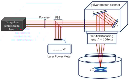
Figure 1.
Femtosecond laser ablation system.
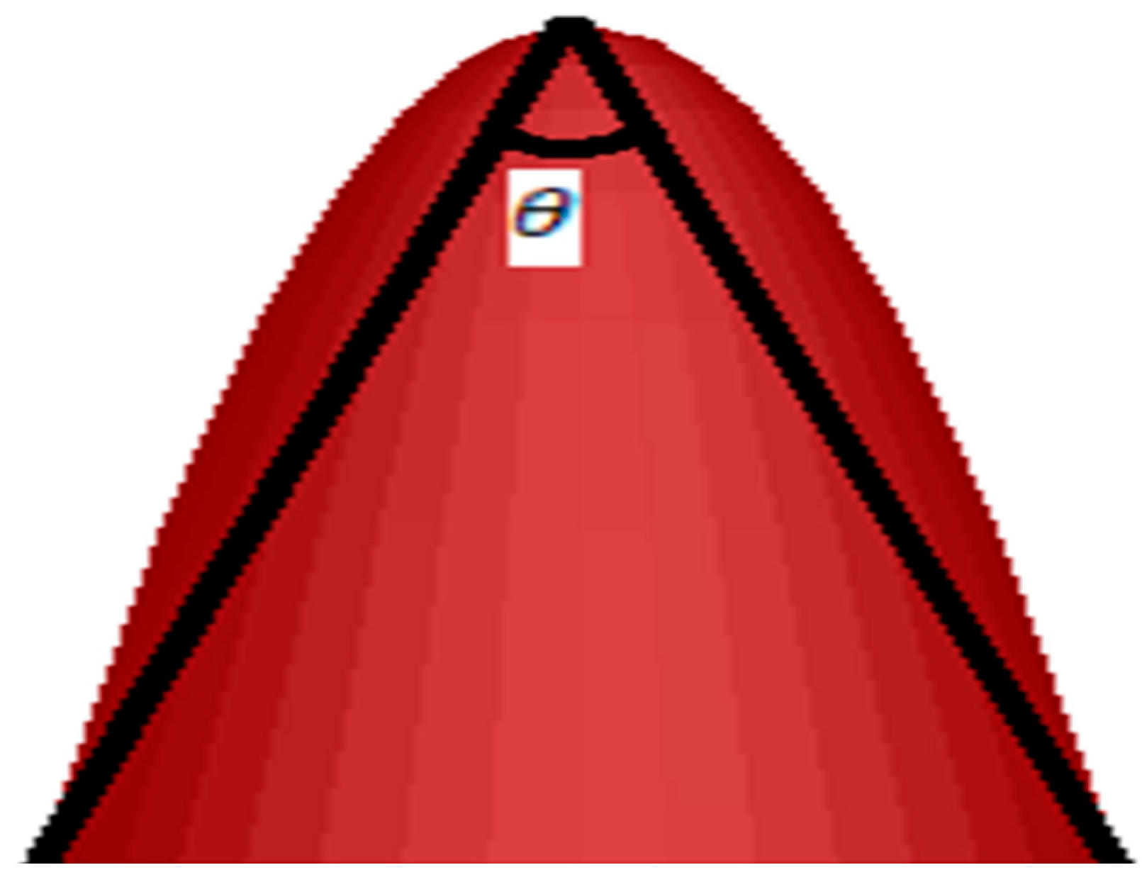
The surface morphology of black silicon was determined by scanning electron microscopy (SEM Zeiss EVO18, German), laser confocal microscopy was used to observe the surface morphology of black silicon, and a statistical analysis of surface morphology parameters was performed. A spectrophotometer (Shimadzu UV-3600 Plus, Japan, total scattered light is measured in the measurement) was employed to characterize the reflectance and transmittance of each black silicon sample. The absorptance (A) in the visible–near-infrared range was calculated using the formula A = 1 – T − R, where R and T represented the reflectance and transmittance, respectively. To further investigate the impact of microstructure parameters on reflectance and transmittance, this study approximated the microstructure as a parabolic cone and simplified the microstructure parameters to the base radius and height (as depicted in Figure 2), described by Equation (1):
where denoted the base radius of the parabolic cone, and represented the height of the parabolic cone. Because the plasma was ejected from the silicon wafer surface by shockwave, the thickness of the substrate correspondingly reduced as the surface morphology of the black silicon improved. In this simulation, we conducted separate simulations where the substrate thickness was independent of the microstructure height and decreased with the variation in the microstructure.
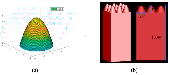
Figure 2.
(a) Parabolic cone schematic. (b) Black silicon microstructure simulation diagram.
A layer of Al film was deposited on the backside of the black silicon by magnetron sputtering of the black silicon after laser ablation. Then, the black silicon underwent high-temperature annealing at 550 for 5 min under vacuum () to repair lattice defects generated during the ablation process [27,28,29,30,31,32]. Simultaneously, the Al film formed Ohmic contact with the surface of the Si wafer under high temperature [32], thereby a p+n junction was created (as illustrated in Figure 3). A reverse bias voltage of −1 was applied to the black silicon photodiode. The dark current and photocurrent of the fabricated black silicon photodiode were characterized using an integrating sphere and a current microampere meter. The light flux received at the sample was measured using a photometer. The spectral responsivity of the device was measured under a −1 bias using light emitted from a 250 W bromine tungsten lamp (GLORIA-T250A, China), and the collected spectra were filtered by a monochromator (Zolix Omni-λ300, China). The Raman spectra of black silicon were measured using a confocal Raman spectrometer (excited by a Horiba scientific-LabRAM HR evolution, 633 , power: 8 , diameter of the laser spot: 1.5 , spectral resolution: 1.3 ) to characterize the number of lattice defects.
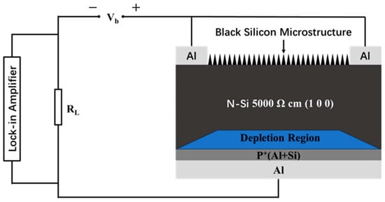
Figure 3.
Schematic diagram of the black silicon photodiode structure.
3. Results and Analysis
3.1. FDTD Simulation Results for Black Silicon
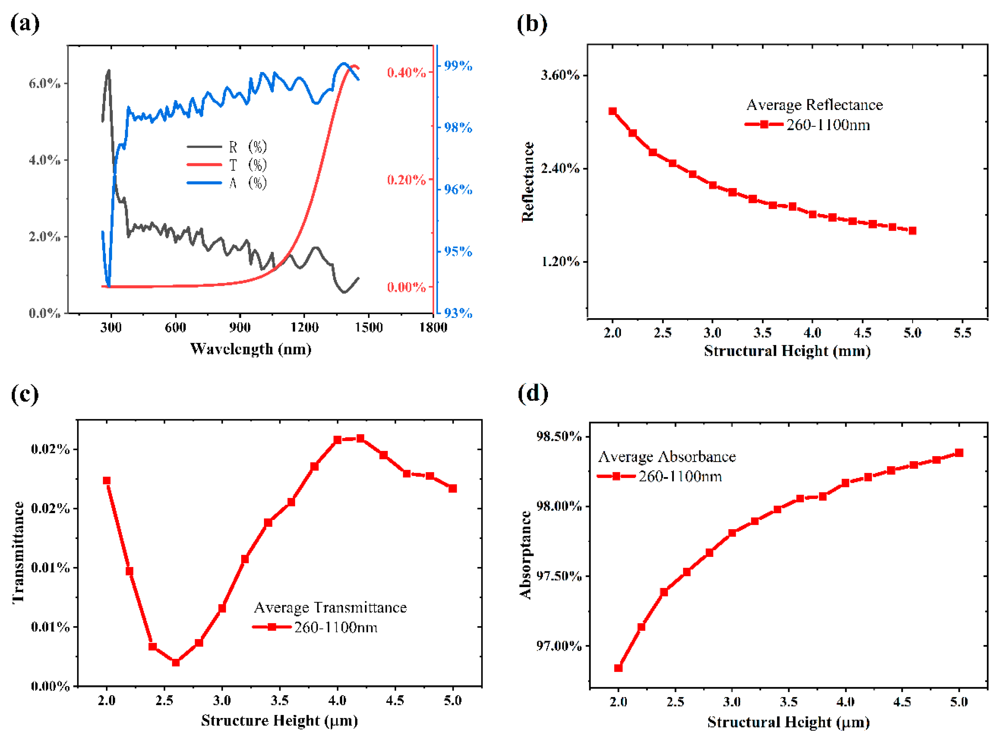
In practical experiments, controlling the parameters of black silicon microstructures by adjusting laser power typically results in simultaneous changes in both the microstructure height () and base radius (). Consequently, it is difficult to determine the individual effects of these parameters on the absorption rate. To address this issue, we employed the finite-difference time-domain (FDTD) method to analyze the absorption rate by varying only one parameter at a time. Ultimately, the two variables were unified into the expression , using variations in to describe the absorption rate of the microstructures, thereby achieving a unified variable approach.
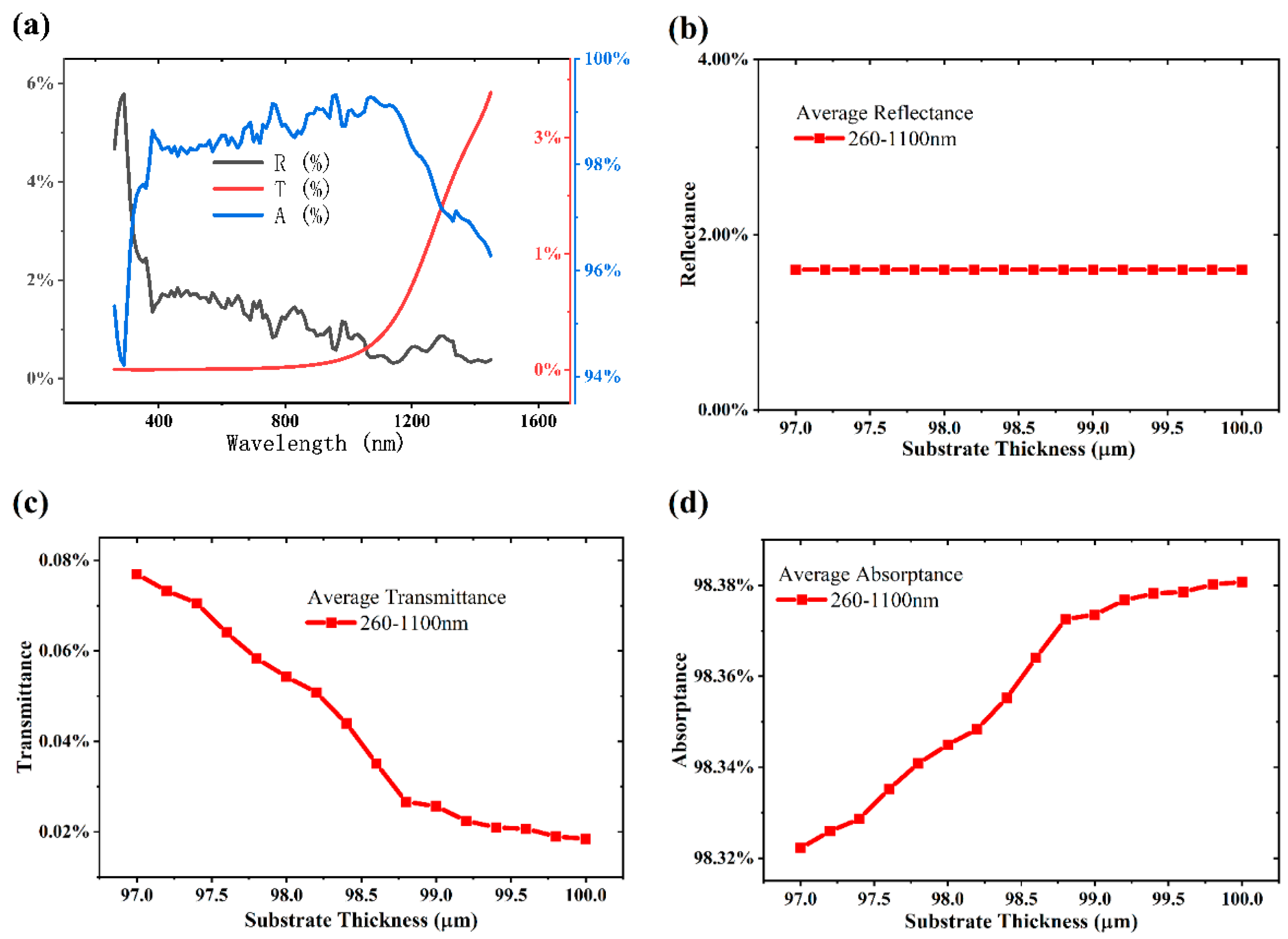
Using FDTD, we simulated the reflectance, absorptance, and transmittance of 16 groups with different heights from 2 to 5 at a 0.2 interval; the radius of the bottom surface was constant at 3 , while the thickness of the substrate was maintained at 100 . As shown in Figure 4a, for the simulation result with a height of 4 μm and a bottom radius of 3 , the absorptance in the 260–1100 band is mainly determined by the reflectivity, which is attributed to the multiple reflections on the surface many times, which results in multiple absorption. As a result, a high absorptance and a transmittance close to 0 are produced in this band. In order to visualize the effect of different microstructures on the absorptivity, as shown in Figure 4b,c, we took the mean change in reflectance, transmittance, and absorptivity of the simulation results in the band from 260 to 1100 as a characterization of the effect of different structural changes on the absorptivity.
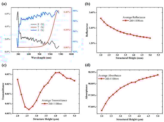
Figure 4.
(a) Reflectance (R), transmittance (T), and absorptance (A) simulation results of FDTD for microstructures (h = 4 μm, r = 3 μm). (b–d) Average reflectance, transmittance, and absorptance of microstructures with different heights in the 260–1100 nm bands.
One can see in Figure 4b that the reflectance decreases as the height of the microstructure increases because of the fact that the number of light reflections in the microstructure increases as the height increases and, correspondingly, as shown in Figure 4d, the absorption rate increases. Interestingly, the refractive indices in both Figure 4c and Figure 5c show a clear inflection point. This phenomenon may be related to the transmission-enhancing effect of the microstructure [33] and the overall thickening of the model in the simulation, which is explained later in the discussion in conjunction with Figure 6. Since the order of magnitude of the transmittance change is very small in the 260–1100 nm band, the effect of the transmittance can be neglected when discussing the absorptivity.
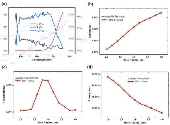
Figure 5.
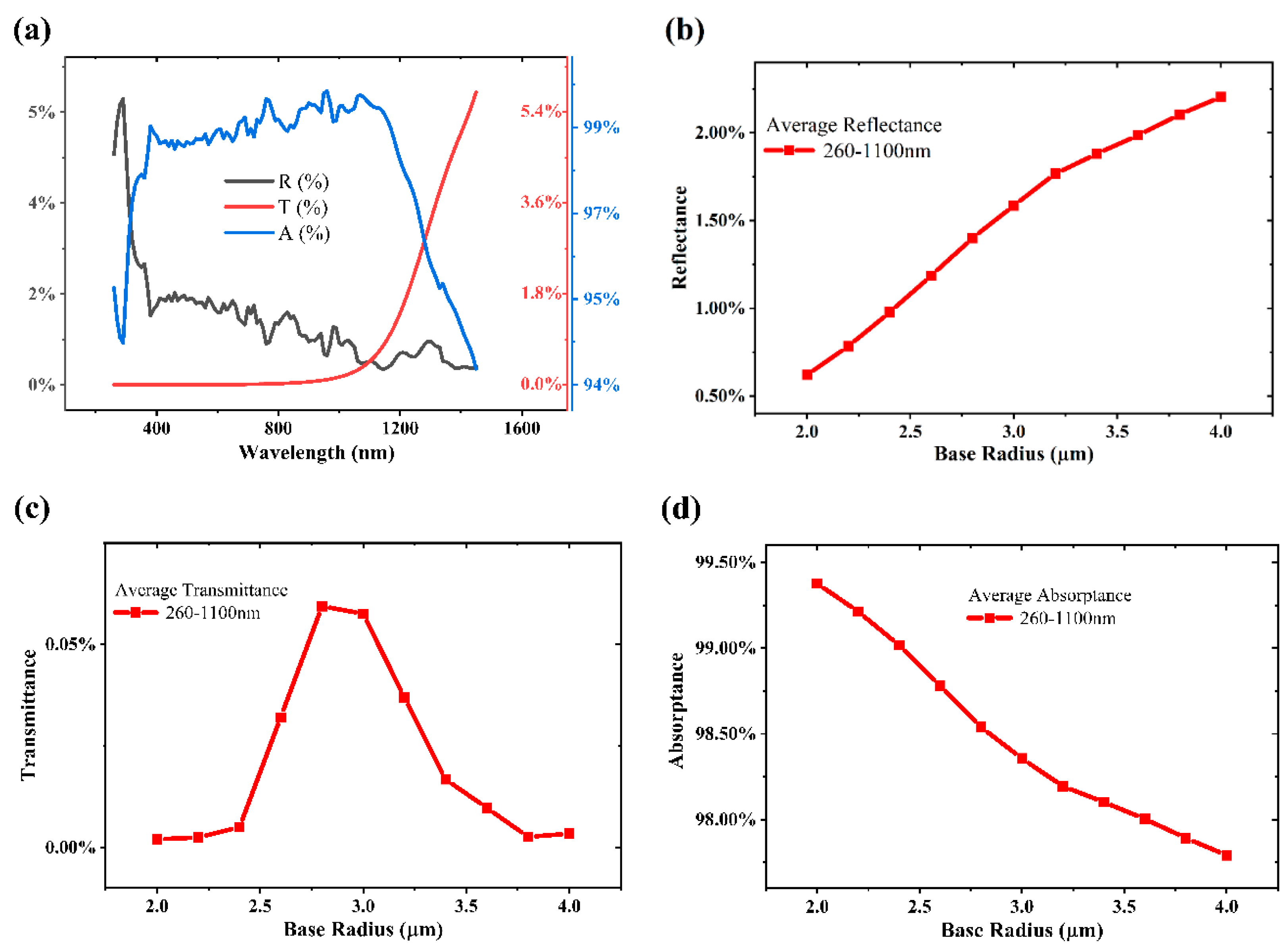
(a) Reflectance (R), transmittance (T), and absorptance (A) simulation results of FDTD for microstructures (h = 5 μm, r = 3 μm). (b–d) Average reflectance, transmittance, and absorptance of microstructures with different bottom radius 260–1100 nm bands.
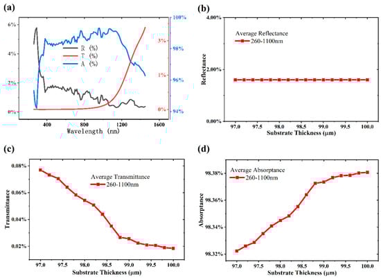
Figure 6.
(a) Reflectance (R), transmittance (T), and absorptance (A) simulation results of FDTD for microstructures (substrate thickness = 98 um, h = 5 μm, r = 3 μm). (b–d) Average reflectance, transmittance, and absorptance of microstructures with different substrate radii for different wavelength bands.
We conducted simulations to study black silicon surface microstructures with different base radii, where the height of the microstructure h = 5 and the radius of the bottom surface r = 2 to 4 . Figure 5 shows the simulation results of reflectivity, transmittance, and absorptance of the microstructures with h = 5 and base r = 3 . The average of each set of simulation results is taken to characterize the effect of substrate radius variation on reflectance, transmittance, and absorptance. In Figure 5b, it can be seen that different substrate radii affect the reflectivity of black silicon. The base radius is inversely proportional to reflectance, with a larger base radius leading to higher reflectance. The average transmittance varies; as shown in Figure 5c, there is an inflection point, similar to Figure 4c, but the transmittance is two orders of magnitude smaller compared with the reflectance, and again, the effect on the absorptance is negligible. As shown in Figure 5d, the variation in the substrate radius of the microstructure affects the reflectivity of the light; the larger the substrate radius, the higher the reflectivity and the lower the absorptance.
In practical experiments, the formation of microstructures is accompanied by substrate thinning due to continuous laser ablation. Therefore, we needed to determine whether thinning the substrate has an effect on the absorptance of black silicon. We employed FDTD simulations to model and simulate the reflectance, absorptance, and transmittance of black silicon with the same microstructure parameters (, ) but varying substrate thicknesses (Substrate thickness =to). Figure 6a shows the simulation results of reflectance, transmittance, and absorptance for the black silicon with substrate thickness, , and . As depicted in Figure 6b, different thicknesses have no impact on reflectance.
Although there is a decreasing trend in the average transmittance (Figure 6c), the magnitude of its transmittance is much smaller compared with the magnitude of reflectance, making its influence on absorptance in this wavelength range negligible. This indicates that during the actual ablation process, the impact of substrate thinning on the transmittance of black silicon is more noticeable compared with the enhanced transmittance in the infrared range due to microstructures. It can be observed in Figure 6d that as the substrate thickness increases, the transmittance of black silicon gradually decreases, with an increase in average absorptance. Combined with Figure 6d, it is shown that in the actual ablation process, although substrate thinning increases the transmittance, its effect on the absorptivity is almost negligible. It can be observed in Figure 6d that the transmittance of black silicon decreases gradually with increasing substrate thickness, leading to an increase in the average absorption.
Although the transmittance variations in Figure 4c and Figure 5c are negligible, their trends suggest the following interesting phenomenon: the variation in the average transmittance is not monotonic, and there is at least one inflection point in it. We speculate that there may be two reasons for this as follows: (i) The presence of microstructures greatly enhances the light trapping ability of the silicon surface, and we can infer that there is a certain degree of transmittance enhancement effect for photons, resulting in an increase in transmittance according to Xiaona Zhao et al. [33] (ii) Figure 4c combined with Figure 6c depicts that the overall thickness of the model in the simulation is thickened because of the fact that the microstructure becomes taller but the thickness of the substrate is not thinned accordingly. This results in two inflection points in the average transmittance in Figure 4c due to the effects of the transmittance enhancement effect and the overall thickening.
Because of the constraints imposed by the bandgap width, silicon (Si) exhibits a lower photon absorptance in the wavelength range exceeding , resulting in the manifestation of an enhanced transmission effect in black silicon. Based on previous arguments, while enhanced transmission can occur within the band gap, its effect is negligible. Therefore, in the ensuing discussion, we focus exclusively on the simulation results within the 260–1100 wavelength range, providing an initial summary of the influence of variations in black silicon surface microstructure parameters on absorptance:
- 1.
- Without considering substrate thinning, an increase in the height of black silicon surface microstructures corresponds to a decrease in reflectance and an increase in absorptance. Similarly, a reduction in the bottom radius of black silicon surface microstructures leads to a decrease in reflectance and an increase in absorptance.
- 2.
- In the wavelength range where the photon energy exceeds the bandgap width of silicon (200 < λ < 1100 ), the majority of incident light is absorbed by black silicon. The primary factor influencing the absorptance of black silicon is the trapped light energy of its surface microstructures, specifically the magnitude of light reflectance. Although there is a certain enhancement in transmittance in this wavelength range, its magnitude can be considered negligible compared with the overall absorptance.
- 3.
- After simulating black silicon with substrate thicknesses of 97 to 100 , we find that substrate thinning increases the transmittance and decreases the absorptance of black silicon, but in the 260–1100 band, the difference in absorptance between the 97 and 100 substrate thicknesses of black silicon is only 0.06%, which is a negligible effect. Meanwhile, it can be observed in Figure 6d that the thicker the substrate, the higher the absorptance, but with the increase in the thickness, the phenomenon of absorptance saturation occurs [33].
During the laser melting process, variations in the ablation laser energy density produce different surface microstructures. In this paper, the structural parameters and h of different black silicon microstructures are characterized. and do not vary independently for each sample, and the relationship between the two and the black silicon absorptance rate varies inversely. Combining the two parameters in the simulations requires the introduction of another microstructural parameter. As shown in Figure 7, by defining the angle at the point where the two bottom and top corners join in the side view of the microstructure at , and can be combined by Equation (2):
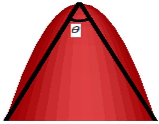
Figure 7.
Side view of a microstructure.
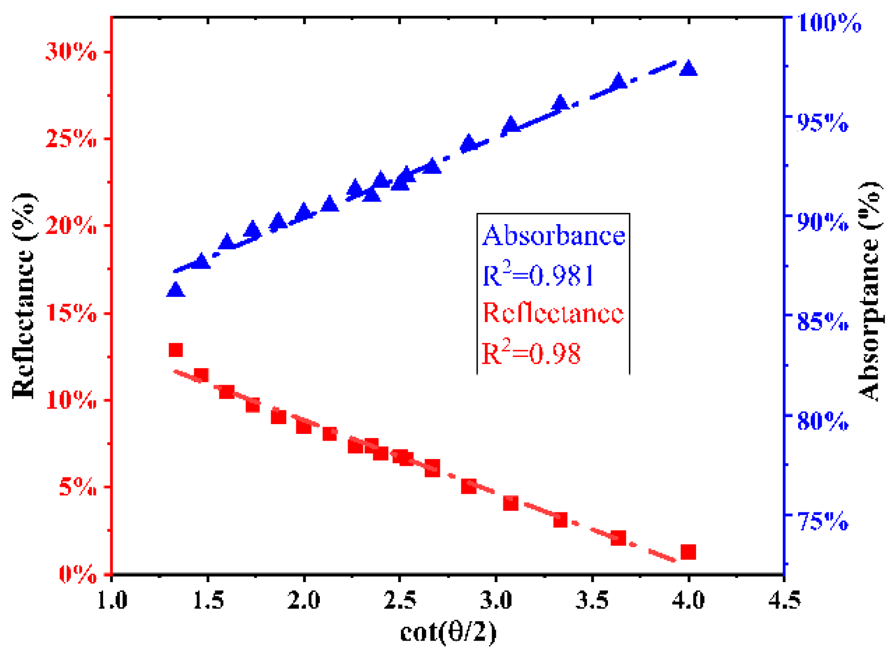
As shown in Figure 8, the different base radii (, ) and different heights (, ) of the microstructures in the above simulation are brought into Equation (2), as the in Figure 8, and the average absorptance rate and reflectivity of the simulation results are taken as the . It can be observed that the reflectivity decreases with the increase in cot, and the absorptance increases. There is a significant linear relationship between the two and cot (correlation coefficient () = 0.981, 0.98).
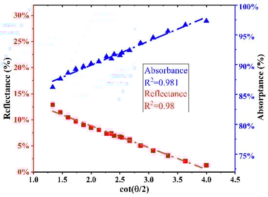
Figure 8.
Comparison of different microstructure parameters () with average absorptance (A) and reflectance (R) (simulation results).
It is evident that with minor variations in microstructure, the apex angle determines the incident angle of incoming light. When not considering the microstructure height and assuming only vertical light incidence, the apex angle should be less than 90° for the occurrence of the third reflection in the structure. This implies that a smaller apex angle or larger enhances the trapping capability of the microstructure. However, when there is a considerable difference in the microstructure height, a trend emerges that was mentioned in previous studies, where larger microstructures correspond to higher absorptance [25]. This is attributed to the increased reflection times of light within the structure with increasing height, thereby enhancing its absorptances.
One can see that with minor variations in the microstructure, the apex angle of the microstructure determines the angle of incidence of incoming light. When not considering the height of the microstructure and solely focusing on perpendicular light incidence, the top angle of the microstructure should be less than 90° for the occurrence of the third reflection within the structure. This implies that a smaller top angle or larger enhances the trapping capability of the microstructure. However, the microstructure size is positively correlated with the absorptance rate when the heights of the microstructures differ significantly. This is attributed to the fact that an increase in the height of the structure similarly increases the number of reflections of light within the structure, thereby enhancing its absorptance.
3.2. Black Silicon Surface Morphology and Its Absorptance
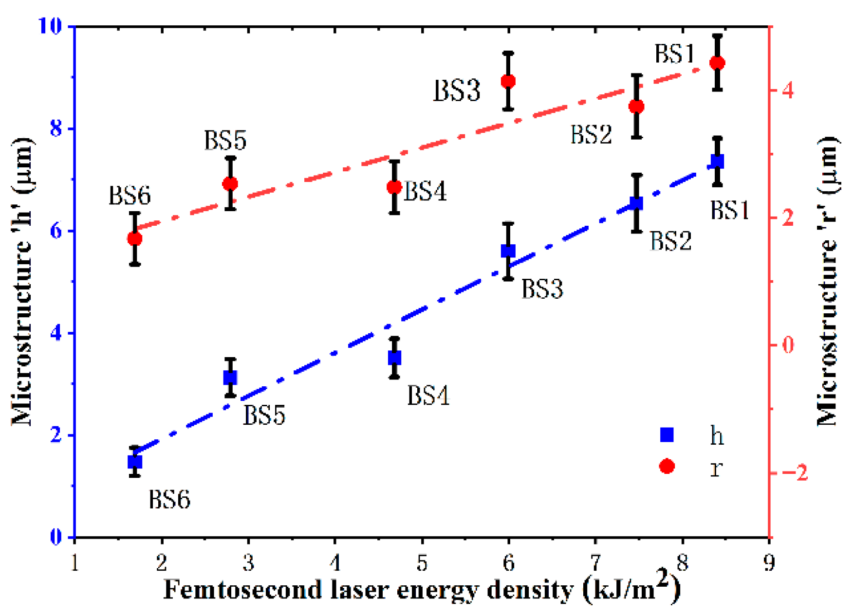
Figure 9 presents SEM images and 3D reconstructions modeled by confocal microscopy of the surface morphologies of six black silicon samples. The overall trend aligned with the pattern described in the literature [25], indicating that larger black silicon microstructures are formed with higher laser energy density, and subtle differences in morphology existed among samples with similar laser energy densities (such as BS1 and BS2; BS4 and BS5). In this paper, microstructural parameters were measured by examining 200 microstructural features on the surface of each sample and averaging the results. This approach reduced the influence of extreme anomalies on the statistical outcomes and highlighted the trends in black silicon microstructural parameters under different laser ablation powers. As can be seen in Figure 10, the variations in the surface microstructural parameters of the samples with similar ablation energies are less than 1 , and such a small range of parameter variations leads to a higher absorption rate of black silicon that is not of the high ablation energy for similar ablation energies, as shown in Figure 11b. Additionally, the 3D images revealed relatively consistent heights. The height (h) and base radius (r) of each black silicon microstructure were measured using both SEM and confocal microscopy, as illustrated in Figure 10. Overall, both h and r increase with the rise in laser energy density. However, the morphological variations among black silicon samples with similar energy densities do not conform to the aforementioned pattern.
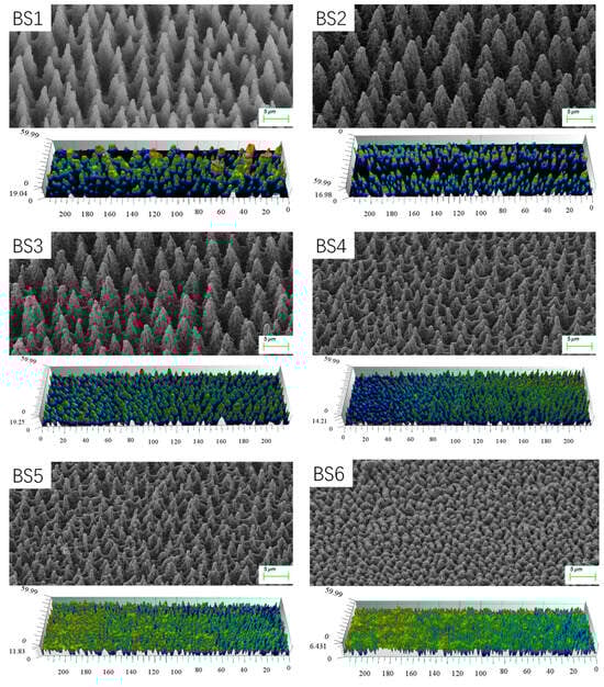
Figure 9.
SEM and confocal microscopy images of the surface morphology of BS1~BS6.

Figure 10.
Average parameter changes in the black silicon surface morphology.
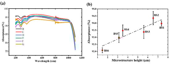
Figure 11.
(a) Absorptance of six black silicon samples. (b) Variation in the average absorptance in the 260–1100 nm band with different microstructure heights of six black silicon samples.
In a previous study [34], it was clearly seen that the absorptance results exhibited in the above bandgap (200–1100 nm) before and after annealing did not change significantly, which suggests that the introduction of S elements and lattice defects are not the main factors affecting the absorptance of the above bandgap. Therefore, the effect of the different doping concentrations of S among the different samples can be neglected in this band. Different morphological characteristics lead to different absorptance in the 200–1100 nm band after annealing at 550 °C, as shown in Figure 11a. In this band, absorptance can be attributed to silicon [13,14]. The former’s absorptance was far higher than that of the latter. Therefore, we ignored the impact of S elements on the absorptance and used the average absorptance of the 200–1100 nm band to discuss the effect of morphology on the absorptances of the black silicon. One can see in Figure 11b that the larger the ablation energy density, the higher the microstructure height, and, as a result, the larger the average absorptance. The overall average absorptance increases with the increase in the microstructure heights, but the opposite variation in the average absorptance is also observed for the two groups of samples with similar heights (BS1 and BS2; BS3 and BS4).
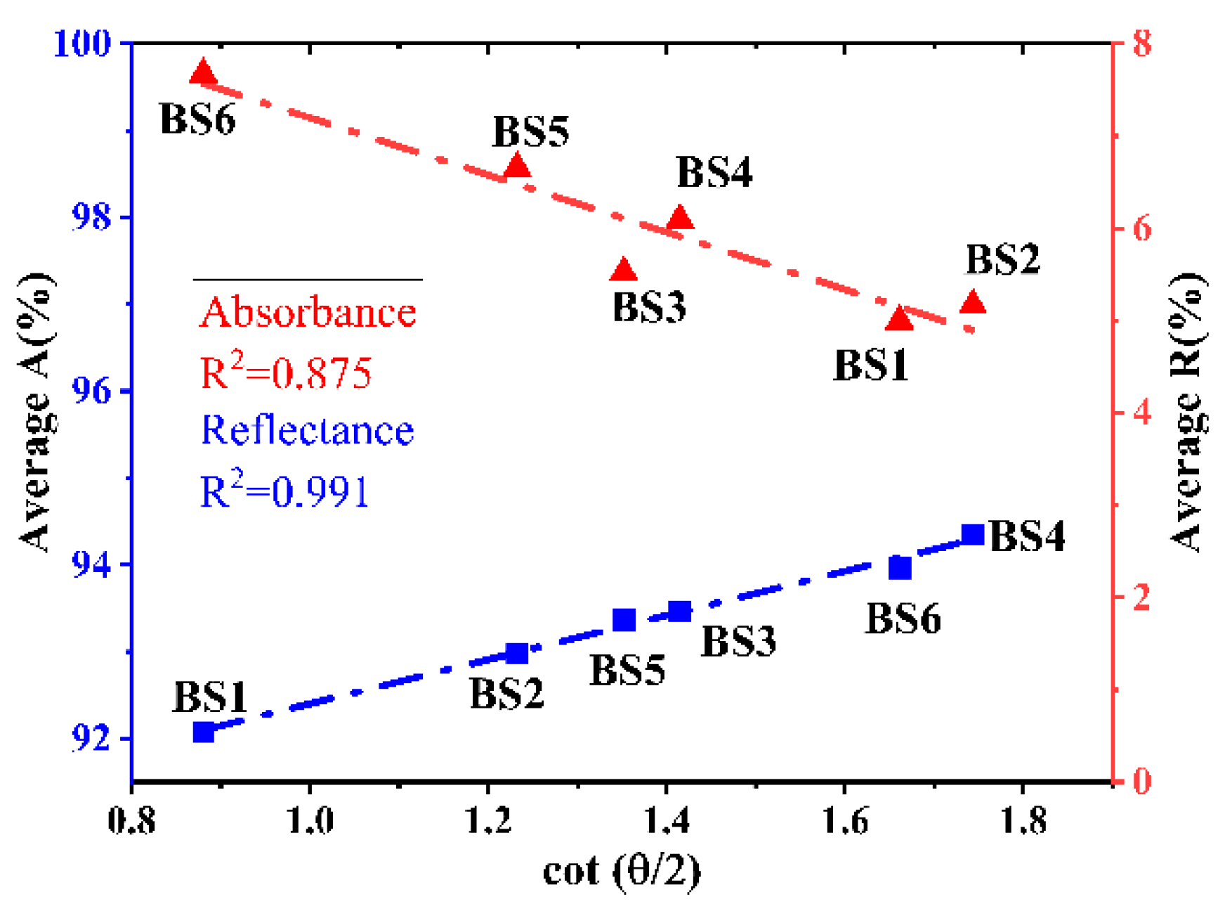
Finally, we measured the microstructure parameters, reflection rates, and absorption rates of six black silicon samples (as shown in Figure 10 and Figure 11). Using the height (h) and base radius (r) obtained from confocal microscopy, these data were substituted into Equation (2), with the results displayed in Figure 12. Figure 12 illustrates the relationship between the average reflection and absorption rates () and the coefficient of the microstructures () for the six black silicon samples (BS1~BS6) across the 260–1100 wavelength range. The fitting coefficient for the reflection rate is as high as 0.99, while for the absorption rate, it is 0.87, indicating that the observed variation patterns are consistent with the simulation results discussed in Section 3.1.
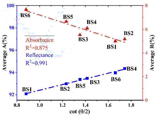
Figure 12.
Comparison between different microstructure parameters () and the average absorptance (A) and reflectance (R) (sample test results).
3.3. Influence of Surface Morphology on the Photoelectric Properties of Black Silicon Photodiodes
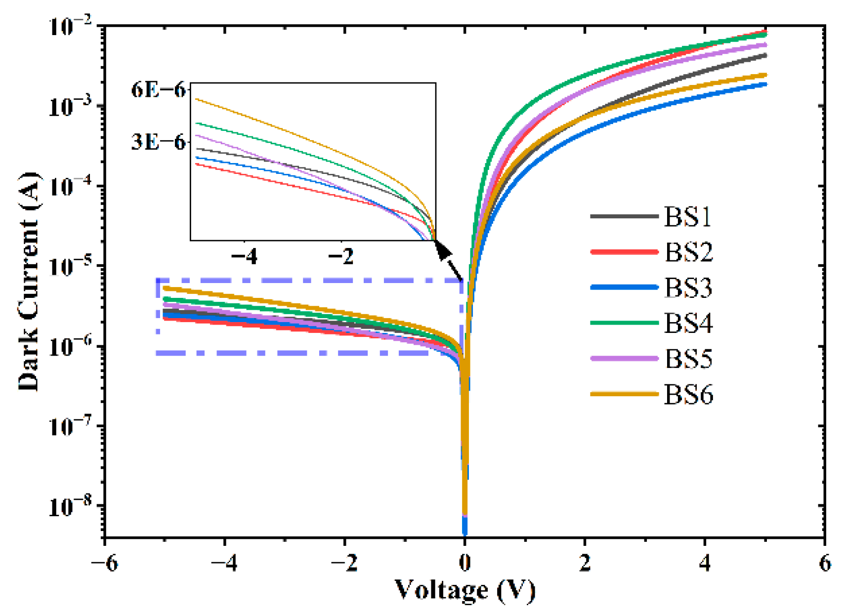
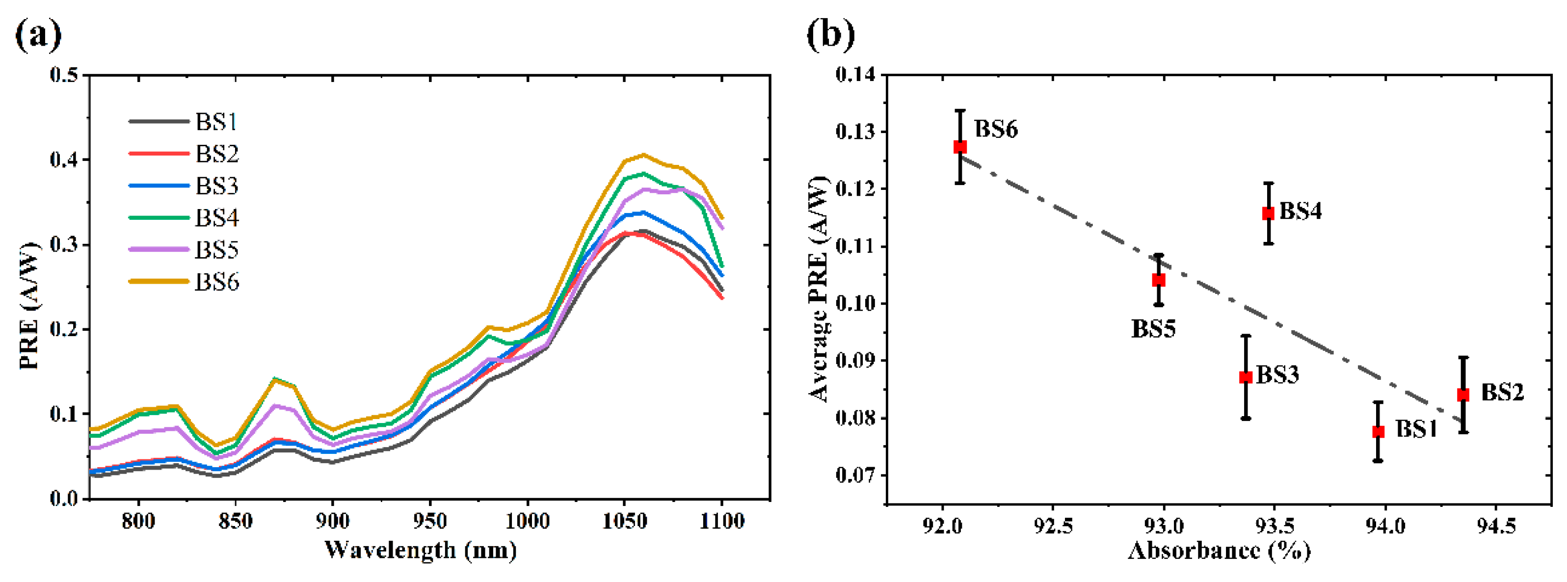
As can be seen in Figure 13, all six black silicon samples show the rectification behaviors of the diode. This indicates that in the Al film sputtered on the backside of the black silicon, after annealing at 550 °C, the Al element doped into the silicon and formed an ohmic contact with the silicon backside, which led to the formation of a p+-n junction. Figure 14a illustrates the photocurrent responses of BS1 to BS6 in the 800–1100 nm wavelength range. In comparison with the absorptance (in Figure 6), it is noteworthy that the highest photocurrent response efficiency was not exhibited for BS1, with the highest absorptance. To further analyze the correlation between the absorptance and photocurrent response, Figure 14b compares the average photocurrent response efficiency and absorptance of BS1 to BS6 in the 800–1100 nm wavelength range. Overall, absorptance presents a downward trend, while photocurrent response efficiency shows an upward trend. And locally, the samples in the BS5 and BS4 and BS3 and BS2 groups conform to the law that the higher the absorptance, the higher the photoelectric response efficiency. This indicates that when laser ablation energy is without a significant difference, the photocurrent response efficiency is primarily influenced by its absorptances, reflecting the impact of microstructure dimensions. However, in some cases with a considerable difference in laser energy density, the influence of absorptance is no longer the primary factor. Then, the factors influencing photoelectric response efficiency become crucial.
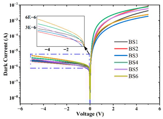
Figure 13.
Current–voltage characteristics of black silicon and unetched silicon photodiodes.

Figure 14.
(a) Optical power current response efficiency (PRE) and (b) variations in average photo-current response efficiency alongside average absorptance changes for six black silicon samples.
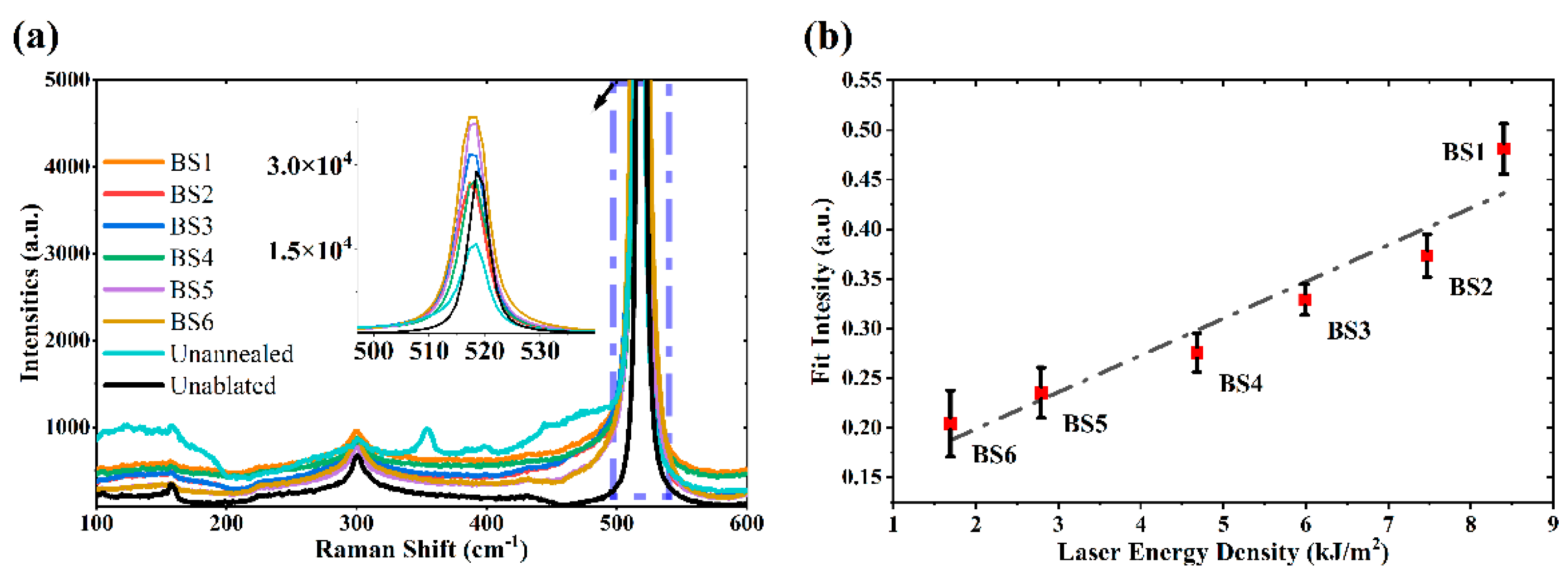
In situations where there is a significant difference in laser energy density, identifying the primary factors influencing photoelectric response efficiency becomes crucial. To address this issue, Raman spectra were obtained for six black silicon samples, as depicted in Figure 15a.
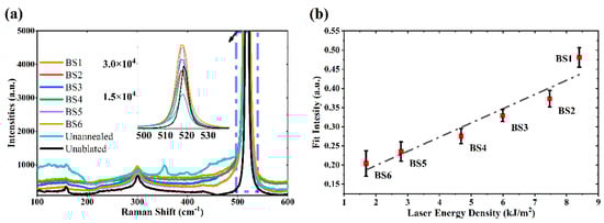
Figure 15.
(a) Raman spectra of six black silicon samples; (b) Raman peak intensity variation located near 520
The peak at 300 is attributed to the TA (transverse acoustic phonon) of Si lattice vibration, which also belongs to Si I, and the peak at 520 cm−1 is attributed to the TO (transverse optical phonon) or LO (longitudinal optical phonon) of Si, while the vibrations of TO and LO of Si are much lager than the vibration of the TA of the silicon. The position of the peak at 520 for black Si is shifted to the left by 1.2 compared with the Raman peak for unablated Si, while the Raman peak after ablation has a wider full width at half height (FWHM) than that of the unablated sample. The shift in the peaks correlates with the change in the surface stress of Si after laser ablation [35], and the shift to the left indicates that the ablated reductive surface lattice is affected by tensile stresses. The FWHM of Si is affected by the surface doping, crystallinity, and defects. More defects make the peaks at 520 wider, but after the same ablation, the spreading width of the Raman spectra of BS1 and BS6 are 6.2 and 6.1 , and the difference is not obvious. Therefore, although the FWHM at 520 of the Raman spectra of black silicon can reflect the changes in the number of defects on the surface of the sample, it is not satisfactory to characterize the changes in the number of defects using this method when laser ablation energies are similar (e.g., two samples of BS1 and BS2, whose FWHMs are almost the same).
The Raman spectra of unannealed BS1 and unprocessed silicon wafers were used as a control group. Compared with the unprocessed silicon wafer, the Raman spectra of the annealed BS1 shows a higher envelope in the range of 320 to 490 , which indicates that some of the lattice defects have not been repaired. Significant polycrystalline silicon peaks (Si-XII (354 and 401 ) and Si-III (389 and 446 )) are observed in the Raman spectra of the unannealed BS1, which are partially repaired after annealing. Their signals are masked by the broadening of the stronger single-crystalline silicon peaks (520 ), but the difference can still be seen from the spectral line variations from 320 to 490 . For Raman spectra, the relationship between the peak intensity and the content of the substance per unit volume is shown in Equation (3) [36]:
where is the intensity of the Si−n(XII or III) Raman lines; N−(Si-n) is the number of molecules of Si−n per unit volume; is the intensity of scattered light per molecule; and k is a coefficient depending on the experimental conditions (optical characteristics of the instrument, spectral sensitivity of the detector, etc.) [36]. From Equation (3), it can be seen that the substance content is positively correlated with the intensity of the corresponding Raman spectrum. Meanwhile, in order to eliminate the influence of experimental conditions on Raman spectra, this paper utilized the internal standard method [37]. Taking the peak at Si−I (520 ) as a calibration, the four peaks at Si-XII (354 and 401 ) and Si-III (389 and 446 ) were pre-processed, and the final Raman spectroscopic polycrystalline silicon spectral intensity was expressed as shown in Equation (4):
Bringing in Equation (3) gives:
It can be seen that the internal standard method can effectively minimize the experimental bias due to the instability of the experimental equipment. Figure 15b shows the relationship between the samples with different laser ablation energies and the relative intensity of polycrystalline silicon spectra in their Raman spectra. The results show that the relative intensity of the Raman signal of polysilicon becomes weaker as the laser ablation energy density decreases, indicating that there are relatively fewer lattice defects.
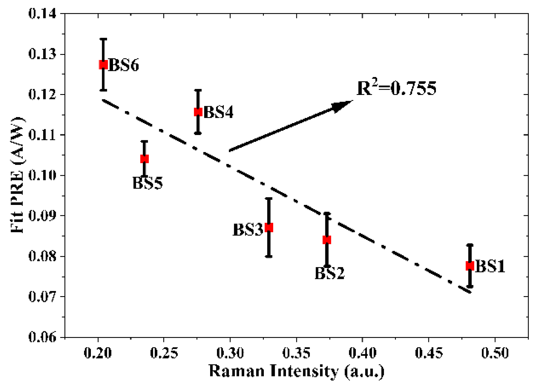
Further, we discussed the variation rule of the number of lattice defects and the photoelectric response efficiency of the black silicon samples. As shown in Figure 16, the x-axis is the relative intensity of the Raman spectra of the lattice defects in the black silicon, and the y-axis is the corresponding average photoelectric response efficiency (Average-PRE (A/W), which can be observed as an inverse correlation with the number of lattice defects in the black silicon. Although higher laser ablation power yields black silicon surface microstructures with better absorption, more surface defects are introduced at the same time, and thus photogenerated carriers and defects create surface recombination, which results in a reduction in photocurrent and a weakening of the photoresponse efficiency. Although some of the lattice defects can be repaired under the same annealing conditions (same annealing temperature and annealing time), the higher laser ablation power introduces a greater number of lattice defects, and more lattice defects remain after annealing. This makes it appear that the photoresponse efficiency is lower even though the absorption rate is higher. In this case, higher annealing temperatures or annealing times may be required [38], or other elements may be introduced for further repair of the lattice [29,39].
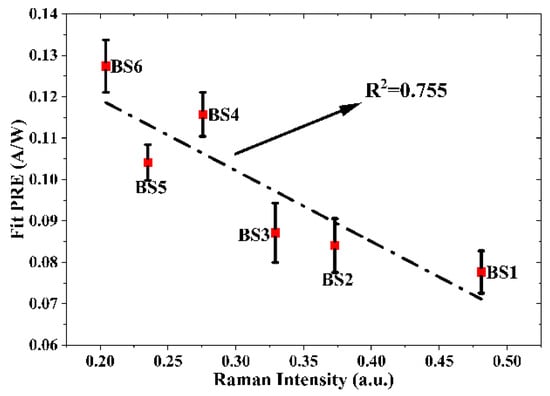
Figure 16.
Variation in the relative intensity (x-axis) of Si-n (XII and III) Raman spectra versus black silicon photoelectric response efficiency (PRE, y-axis).
4. Conclusions
This paper characterizes the surface microstructure parameters of black silicon, absorptance, and the photoelectric response efficiency of black silicon photodiodes to study the relationships among them. The simulation results revealed that the absorptance of black silicon is inversely proportional to the base radius () and directly proportional to the height () of the microstructure. A comprehensive description of the microstructure parameters was achieved through and , which was directly proportional to the absorptance of the microstructure. Simultaneously, characterization of the microstructure parameters and absorptance of black silicon samples revealed that in practical situations, these parameters generally followed the mentioned trends. We collected Raman spectra for six black silicon samples to characterize lattice defects introduced by femtosecond laser ablation. It was found that lattice defects significantly impact the photoelectric response efficiency of devices, and in the femtosecond laser ablation process, higher laser energy density introduces more lattice defects. This is identified as a primary influencing factor of the photoelectric response efficiency of black silicon photodiodes.
Author Contributions
Conceptualization, X.Z. (Xiaomi Zhang); methodology, X.Z. (Xiaomi Zhang); software, X.Z. (Xiaomi Zhang); validation, W.L. and X.Z. (Xiangping Zhu); formal analysis, X.Z. (Xiaomi Zhang); investigation, X.Z. (Xiaomi Zhang); resources, X.Z.(Xiangping Zhu).; data curation, X.Z. (Xiaomi Zhang); writing—original draft preparation, X.Z. (Xiaomi Zhang).; writing—review and editing, X.Z. (Xiaomi Zhang), Y.C., F.L., N.W., B.W. and R.Z.; visualization, X.Z. (Xiaomi Zhang); supervision, W.L., C.J., X.Z. (Xiangping Zhu) and W.Z.; project administration, X.Z. (Xiangping Zhu); funding acquisition, X.Z. (Xiangping Zhu) and C.J. All authors have read and agreed to the published version of the manuscript.
Funding
This research was funded by the National Natural Science Foundation of China (52127817); the research and development project of scientific research instruments and equipment of the Chinese Academy of Sciences (ZDKYYQ20220007); the Natural Science Basic Research Program of Shaanxi (2023-JC-QN-0747); the Key Research and Development Program of Shaanxi (2021LLRH-03); and the National Natural Science Foundation of China (62375224).
Institutional Review Board Statement
Not applicable.
Informed Consent Statement
Not applicable.
Data Availability Statement
The data presented in this study are available from the corresponding author upon request.
Conflicts of Interest
The authors declare no conflicts of interest.
References
- Zheng, J.P.; Jiao, K.L.; Shen, W.P.; Anderson, W.A.; Kwok, H.S. Highly sensitive photodetector using porous silicon. Appl. Phys. Lett. 1992, 61, 459–461. [Google Scholar] [CrossRef]
- Otto, M.; Algasinger, M.; Branz, H.; Gesemann, B.; Gimpel, T.; Füchsel, K.; Käsebier, T.; Kontermann, S.; Koynov, S.; Li, X. Black silicon photovoltaics. Adv. Opt. Mater. 2015, 3, 147–164. [Google Scholar] [CrossRef]
- Liu, X.; Coxon, P.R.; Peters, M.; Hoex, B.; Cole, J.M.; Fray, D.J. Black silicon: Fabrication methods, properties and solar energy applications. Energy Environ. Sci. 2014, 7, 3223–3263. [Google Scholar] [CrossRef]
- Fan, Z.; Cui, D.; Zhang, Z.; Zhao, Z.; Chen, H.; Fan, Y.; Li, P.; Zhang, Z.; Xue, C.; Yan, S. Recent progress of black silicon: From fabrications to applications. Nanomaterials 2020, 11, 41. [Google Scholar] [CrossRef]
- Ma, L.L.; Zhou, Y.C.; Jiang, N.; Lu, X.; Shao, J.; Lu, W.; Ge, J.; Ding, X.M.; Hou, X.Y. Wide-band “black silicon” based on porous silicon. Appl. Phys. Lett. 2006, 88, 171907. [Google Scholar] [CrossRef]
- Wu, J.; Jiang, Q.; Chen, S.; Tang, M.; Mazur, Y.I.; Maidaniuk, Y.; Benamara, M.; Semtsiv, M.P.; Masselink, W.T.; Sablon, K.A.; et al. Monolithically integrated InAs/GaAs quantum dot mid-infrared photodetectors on silicon substrates. Acs Photonics 2016, 3, 749–753. [Google Scholar] [CrossRef]
- Martin, T.; Dixon, P.; Gagliardi, M.A.; Masaun, N. 320×240 pixel InGaAs/InP focal plane array for short-wave infrared and visible light imaging. In Semiconductor Photodetectors II; SPIE: Bellingham, WA, USA, 2005; Volume 5726, pp. 85–91. [Google Scholar]
- Miao, Y.; Wang, G.; Kong, Z.; Xu, B.; Zhao, X.; Luo, X.; Lin, H.; Dong, Y.; Lu, B.; Dong, L. Review of Si-based GeSn CVD growth and optoelectronic applications. Nanomaterials 2021, 11, 2556. [Google Scholar] [CrossRef]
- Liu, S.J.; Chu, J.H. Theoretical study of monolithic dielectric bolometer by thermal diffusion equation. In Infrared Components and Their Applications; SPIE: Bellingham, WA, USA, 2005; Volume 5640, pp. 49–53. [Google Scholar]
- Feldman, A. Algorithm for solutions of the thermal diffusion equation in a stratified medium with a modulated heating source. High Temperatures-High Pressures 1999, 31, 293–298. [Google Scholar] [CrossRef]
- Her, T.-H.; Finlay, R.J.; Wu, C.; Deliwala, S.; Mazur, E. Microstructuring of silicon with femtosecond laser pulses. Appl. Phys. Lett. 1998, 73, 1673–1675. [Google Scholar] [CrossRef]
- Jin, X.; Sun, Y.; Wu, Q.; Jia, Z.; Huang, S.; Yao, J.; Huang, H.; Xu, J. High-performance free-standing flexible photodetectors based on sulfur-hyperdoped ultrathin silicon. ACS Appl. Mater. Interfaces 2019, 11, 42385–42391. [Google Scholar] [CrossRef]
- Dong, B.; Wang, W.; Liu, X.-L.; Li, H.; Li, Y.; Huang, Y.; Ning, X.; Zhao, L.; Zhuang, J. Light and gas dual-function detection and mutual enhancement based on hyperdoped black silicon. Optics Express 2024, 32, 13384–13395. [Google Scholar] [CrossRef] [PubMed]
- Bardalen, E.; Bouchouri, A.; Akram, M.N.; Nguyen, H.-V. Black Silicon as Anti-Reflective Structure for Infrared Imaging Applications. Nanomaterials 2023, 14, 20. [Google Scholar] [CrossRef]
- Zhang, Y.; Loh, J.Y.; Kherani, N.P. Facilely Achieved Self-Biased Black Silicon Heterojunction Photodiode with Broadband Quantum Efficiency Approaching 100%. Adv. Sci. 2022, 9, 2203234. [Google Scholar] [CrossRef] [PubMed]
- Kalem, S. Time-resolved radiative recombination in black silicon. J. Mater. Sci. Mater. Electron. 2023, 34, 724. [Google Scholar] [CrossRef]
- Wu, S.; Chen, Q.; Zhang, L.; Ren, H.; Zhou, H.; Hu, L.; Tan, C.S. Wafer-scale nanostructured black silicon with morphology engineering via advanced Sn-assisted dry etching for sensing and solar cell applications. Nanoscale 2023, 15, 4843–4851. [Google Scholar] [CrossRef]
- Kim, J.; Lee, J.; Lee, J.M.; Facchetti, A.; Marks, T.J.; Park, S.K. Recent Advances in Low-Dimensional Nanomaterials for Photodetectors. Small Methods 2024, 8, 2300246. [Google Scholar] [CrossRef]
- Zhao, J.-H.; Li, X.-B.; Chen, Q.-D.; Chen, Z.-G.; Sun, H.-B. Ultrafast laser-induced black silicon, from micro-nanostructuring, infrared absorption mechanism, to high performance detecting devices. Mater. Today Nano 2020, 11, 100078. [Google Scholar] [CrossRef]
- Holton, W.C.; Cavin, R. A perspective on CMOS technology trends. Proc. IEEE 1986, 74, 1646–1668. [Google Scholar] [CrossRef]
- Ma, S.; Liu, S.; Xu, Q.; Xu, J.; Lu, R.; Liu, Y.; Zhong, Z. A theoretical study on the optical properties of black silicon. AIP Adv. 2018, 8, 035010. [Google Scholar] [CrossRef]
- Rahman, T.; Boden, S.A. Optical modeling of black silicon for solar cells using effective index techniques. IEEE J. Photovolt. 2017, 7, 1556–1562. [Google Scholar] [CrossRef]
- Elsayed, A.A.; Sabry, Y.M.; Marty, F.; Bourouina, T.; Khalil, D. Optical modeling of black silicon using an effective medium/multi-layer approach. Opt. Express 2018, 26, 13443–13460. [Google Scholar] [CrossRef] [PubMed]
- Schäfer, S.; McKearney, P.; Paulus, S.; Kontermann, S. Analytical model for extracting optical properties from absorptance of femtosecond-laser structured hyperdoped silicon. J. Appl. Phys. 2022, 131, 243102. [Google Scholar] [CrossRef]
- Wu, C.; Crouch, C.; Zhao, L.; Carey, J.; Younkin, R.; Levinson, J.; Mazur, E.; Farrell, R.; Gothoskar, P.; Karger, A. Near-unity below-band-gap absorption by microstructured silicon. Appl. Phys. Lett. 2001, 78, 1850–1852. [Google Scholar] [CrossRef]
- Apel, C.; Meister, J.; Ioana, R.; Franzen, R.; Hering, P.; Gutknecht, N. The ablation threshold of Er: YAG and Er: YSGG laser radiation in dental enamel. Lasers Med. Sci. 2002, 17, 246–252. [Google Scholar] [CrossRef] [PubMed]
- Parker, G.; Bonar, J.; Starbuck, C. Long incubation times for selective epitaxial growth of silicon using silane only. Electron. Lett. 1991, 27, 1595–1597. [Google Scholar] [CrossRef]
- Wang, W.; Ma, S.; Liu, X.; Zhao, Y.; Li, H.; Li, Y.; Ning, X.; Zhao, L.; Zhuang, J. NO2 gas sensor with excellent performance based on thermally modified nitrogen-hyperdoped silicon. Sens. Actuators B Chem. 2022, 354, 131193. [Google Scholar] [CrossRef]
- Tabbal, M.; Kim, T.; Woolf, D.N.; Shin, B.; Aziz, M.J. Fabrication and sub-band-gap absorption of single-crystal Si supersaturated with Se by pulsed laser mixing. Appl. Phys. A 2010, 98, 589–594. [Google Scholar] [CrossRef]
- Ma, S.-X.; Liu, X.-L.; Sun, H.-B.; Zhao, Y.; Hu, Y.; Ning, X.-J.; Zhao, L.; Zhuang, J. Enhanced responsivity of co-hyperdoped silicon photodetectors fabricated by femtosecond laser irradiation in a mixed SF 6/NF 3 atmosphere. JOSA B 2020, 37, 730–735. [Google Scholar] [CrossRef]
- Crouch, C.H.; Carey, J.E.; Warrender, J.M.; Aziz, M.J.; Mazur, E.; Génin, F.Y. Comparison of structure and properties of femtosecond and nanosecond laser-structured silicon. Appl. Phys. Lett. 2004, 84, 1850–1852. [Google Scholar] [CrossRef]
- Neudeck, G.; Thompson Jr, H.; Schwartz, R. High-Frequency Noise in Germanium-Silicon n-n Heterojunctions. J. Appl. Phys. 1969, 40, 4108–4114. [Google Scholar] [CrossRef]
- Zhao, X.; Zhao, B.; Lin, K.; Nivas, J.J.; Amoruso, S.; Du, W.; Wang, X. Direct fabrication of black Si with enhanced infrared transmittance using femtosecond laser irradiation. Opt. Laser Technol. 2024, 168, 109881. [Google Scholar] [CrossRef]
- James, R.; Schweig, E.; Smith, D.; McGill, T. Experimental investigation of the infrared absorption saturation in p-type germanium and silicon. Appl. Phys. Lett. 1982, 40, 231–233. [Google Scholar] [CrossRef]
- Del Corro, E.; Taravillo, M.; Baonza, V.G. Nonlinear strain effects in double-resonance Raman bands of graphite, graphene, and related materials. Phys. Rev. B—Condens. Matter Mater. Phys. 2012, 85, 033407. [Google Scholar] [CrossRef]
- Golovkin, B. Quantitative analysis of solid-phase mixtures by Raman spectroscopy. J. Appl. Spectrosc. 2008, 75, 444–447. [Google Scholar] [CrossRef]
- Shen, W.; Lin, X.; Jiang, C.; Li, C.; Lin, H.; Huang, J.; Wang, S.; Liu, G.; Yan, X.; Zhong, Q. Reliable quantitative SERS analysis facilitated by core–shell nanoparticles with embedded internal standards. Angew. Chem. Int. Ed. 2015, 54, 7308–7312. [Google Scholar] [CrossRef]
- Carey, J.E.; Crouch, C.H.; Shen, M.; Mazur, E. Visible and near-infrared responsivity of femtosecond-laser microstructured silicon photodiodes. Opt. Lett. 2005, 30, 1773–1775. [Google Scholar] [CrossRef]
- Wang, Y.; Gao, J.; Yang, H.; Wang, X. Near-infrared absorption enhancement in microstructured silicon by Ag film deposition. J. Mater. Sci. Mater. Electron. 2016, 27, 9002–9007. [Google Scholar] [CrossRef]


Disclaimer/Publisher’s Note: The statements, opinions and data contained in all publications are solely those of the individual author(s) and contributor(s) and not of MDPI and/or the editor(s). MDPI and/or the editor(s) disclaim responsibility for any injury to people or property resulting from any ideas, methods, instructions or products referred to in the content. |
© 2024 by the authors. Licensee MDPI, Basel, Switzerland. This article is an open access article distributed under the terms and conditions of the Creative Commons Attribution (CC BY) license (https://creativecommons.org/licenses/by/4.0/).