Article

Logic Gate Generation in a Monostable Optical System: Improving the Erbium-Doped Fiber Laser Reconfigurable Logic Operation

by
Samuel Mardoqueo Afanador-Delgado
1,
José Luis Echenausía-Monroy
2,*,
Guillermo Huerta-Cuellar
3,
Juan Hugo García-López
3,
Erick Emiliano Lopez-Muñoz
3 and
Rider Jaimes-Reátegui
3,*
1
Biomedical Optics Laboratory, CULagos, Universidad de Guadalajara, Centro Universitario de los Lagos, Enrique Díaz de León 1144, Paseos de la Montaña, Lagos de Moreno 47460, Mexico
2
Applied Physics Division, Center for Scientific Research and Higher Education at Ensenada (CICESE), Carr. Ensenada-Tijuana 3918, Zona Playitas, Ensenada 22860, Mexico
3
Dynamical Systems Laboratory, CULagos, Universidad de Guadalajara, Centro Universitario de los Lagos, Enrique Díaz de León 1144, Paseos de la Montaña, Lagos de Moreno 47460, Mexico
*
Authors to whom correspondence should be addressed.
Photonics 2024, 11(12), 1103; https://doi.org/10.3390/photonics11121103
Submission received: 2 October 2024 / Revised: 10 November 2024 / Accepted: 19 November 2024 / Published: 22 November 2024

Abstract

:
A logic gate is typically an electronic device with a Boolean or other type of function, e.g., adding or subtracting, including or excluding according to its logical properties. They can be used in electronic, electrical, mechanical, hydraulic, and pneumatic technology. This paper presents a new method for generating logic gates based on optical systems with an emission frequency equal to that used in current telecommunications systems. It uses an erbium-doped fiber laser in its monostable operating region, in contrast to most results published in the literature, where multistable behavior is required to induce dynamic changes, and where a DC voltage signal in the laser pump current provides the control between obtaining the different logic operations. The proposed methodology facilitates the generation of the gates, since it does not require taking the optical system to critical power levels that could damage the components. It is based on using the same elements that the EDFL requires to operate. The result is a system capable of generating up to five stable and robust logic gates to disturbances validated in numerical simulation and experimental setup. This eliminates the sensitivity to the initial conditions affecting the possible logic gates generated by the system and the need to add noise to the system (as is performed in works based on stochastic logic resonance). The experimental observations confirm the numerical results and open up new aspects of using chaotic systems to generate optical logic gates without bistable states.

1. Introduction

Logic gates are fundamental elements of digital circuits that go back to the Boolean algebra developed by George Boole in the 19th century, and are defined as transistors arranged in special configurations to form electronic circuits. These circuits provide voltage signals as output signals in Boolean form, which result from binary logical operations such as addition and multiplication. Depending on their logical properties, they negate, affirm, include, or exclude. A logic gate performs a logical operation on one or more binary inputs (two possible states) to produce a binary output, with AND, OR, NOT, NAND, NOR, XOR, and XNOR being the most important logic gates. Practical application began in the 1930s with Claude Shannon, who demonstrated how electrical circuits could perform logical operations. The invention of the transistor in 1947 revolutionized the field and enabled the development of more efficient and compact logic gates. Later, in the 1960s, the integration of transistors into integrated circuits led to significant advances in the miniaturization and efficiency of electronic devices. Today, logic gates are used in applications such as computers, smartphones, industrial control systems and automobiles [1,2,3].
In the early 2010s, researchers observed that a bistable dynamical system stimulated with two square waves as input can produce a logical output. The probability of obtaining one of the two possible solutions is controllable by the interaction between the noise level induced in the system and the behavior of the intrinsic nonlinearity of the bistable dynamical system. As the noise intensity increases, the probability that the output represents an operation (think of a NOR/OR gate) also increases until an optimal noise threshold is reached. Beyond this point, the probability drops back to zero if the noise is much higher than the threshold, resulting in the logic output control having a Gaussian profile. This concept, which characterizes logic gates based on dynamic systems with noise, is called Logic Stochastic Resonance (LSR).
Examples of results obtained using this principle are those published in [4,5,6,7], in which, using a bistable dynamic system with a cubic nonlinear function and quadratic-type control inputs, they achieve stochastic resonance behavior by implementing a simple electronic circuit based on a resistor, a capacitor and four CMOS transistors, thus laying the foundation for reconfigurable logic devices.
Considering that chaotic behaviors are practically universal, which in turn are described by deterministic systems with a high sensitivity to the initial conditions and which usually generate an infinite number of patterns and strange attractors, the idea of logic gates based on chaotic systems was developed [8], where the authors managed to obtain all the basic gates that can be quickly and arbitrarily interchanged by thresholding the noise level to switch between the available gates, coining the term chaogate.
Under the premise of exploiting the versatility of chaos in developing logic gates, researchers developed a Set–Reset (SR) flip-flop using NOR gates and implemented it with a Chua circuit [9]. Reference [10] describes the implementation of basic logic gates using a logistic map. In [11], a NOR gate is realized by threshold control in chaotic systems. A circuit with a dynamic logic architecture containing NOR, NAND, and XOR gates is presented in [12], or the approach of a reconfigurable voltage-dependent logic gate based on the equation of a plane [13]. Most of the logic gates described above are based on using chaotic systems with two attractors located at different equilibrium points. This allows a dynamic discretization that considers the system’s response to some distortion and the change in behavior due to the position of the attractor [14,15].
Since the invention and development of the laser (an acronym for Light Amplification by Stimulated Emission of Radiation), based on the theory of stimulated emission proposed by Albert Einstein in 1917, its use and commercialization developed rapidly in the mid-twentieth century. In 1960, Theodore H. Maiman built the first pulsed laser from a pink ruby, ushering in an era of technological innovation. Given the wide range of applications for using and commercializing this type of device, researchers conducted intensive studies find better amplification possibilities and to improve the properties and performance of lasers. In the 1970s, for example, scientists such as Charles K. Kao developed optical fibers that enabled the efficient transmission of light over long distances and laid the foundation for modern telecommunications; today, lasers doped with rare earths are an essential part of telecommunications and medicine.
Rare earths used in doping fiber lasers are a group of 17 chemical elements in the periodic table, including the 15 lanthanides. Their use and research began in the early 1970s. The development of the erbium-doped fiber amplifier in the mid-1980s was the turning point in using this type of element to improve beam efficiency, stability, and quality and to create new types of fiber lasers that can operate at different wavelengths. From the group of lanthanides, erbium is one of the most commonly used elements for doping optical fibers due to its emission properties in the wavelength range of 1550 nm, which coincides with a low-loss window for telecommunications.
Currently, the combination of logic gates and lasers is a promising area that enables high-speed information manipulation over the same communication channel, eliminating the need for analog components and increasing the possibilities of data processing with an outlook to the development of optical and quantum computers. At the intersection of these two disciplines, researchers have found results such as a logical OR (NOR) gate in a laser system. By injecting two digital signals into the optical system, they obtain a response resembling a logical operation [16]. In [17], they show that in a vertical cavity surface-emitting laser with orthogonal optical injection, there is a wide range of noise intensities where the success probability of the logic gate function is equal to one. They also demonstrate that intrinsic laser noise and external noise can be utilized to improve the performance of the logic operation. In [18], they encode two logic inputs into the amplitude of light from a sampled grating distributed Bragg reflector laser and decode two logic output responses into the polarization components emitted by the laser, obtaining a parallel data selection. This result was extended to obtain a reconfigurable flip-flop by a digital signal [19].
Recent research has focused on designing all-optical NOT and XOR logic gates using 2D photonic crystals for applications in optical integrated circuits [20]. Various structures have been proposed, including those based on interference effects [21], based on ring resonators with three inputs [22,23], and linear resonant cavities [24]; where the main goal is to achieve high contrast ratios, fast response times, and high data transfer rates. Although the results are promising and open new perspectives for developing logic gates based on optical systems, the described schemes are not reconfigurable, and the results are limited to numerical experiments without overcoming the hurdle of physical implementation.
Moreover, recent results in erbium-doped fiber laser systems exploit the dynamic richness of the oscillator, particularly in the multistable regions, to characterize the system response and obtain up to three reconfigurable logic gates [25]. In this work, the authors encoded two digital inputs that were de-corelated with each other, while the fiber laser operated in the multistable region. Thus, three functional logic gates were generated and validated numerically and experimentally.
Under the premise of improving the performance of logic gates previously obtained by [25], this article addresses a new and more straightforward way to obtain reconfigurable logic gates in an erbium-doped optical fiber system. On this occasion, we studied the behavior of the laser in a monostable regime, in contrast to another works in the literature that obtain logic gates based on at least bistable dynamic systems. We encoded the digital inputs at the input of the laser system, and characterized the obtained logic response by varying the DC voltage at the modulation input of the optical system. The result is a more robust and efficient logic gate, and a more significant number of operations in a single system. This approach achieved up to five logic operations in the system, compared to the three gates obtained in previous implementations. The experiment validates the numerical results obtained and confirms the good functioning and robustness of the logic gates obtained.
The following parts of the article describe the behavior of the Erbium-Doped Fiber Laser (EDFL), the coefficients that describe its numerical behavior, and the physical elements that make up the experimental implementation. The procedure to characterize the response of the laser considering the different logical operations is described in the third Section 2. The results obtained (both numerically and experimentally) are described in Section 3. A discussion of the results obtained follows, and the manuscript closes with the conclusions and implications of the work.

2. Materials and Methods

2.1. Numerical Model

The dynamics of an EDFL are described by the normalized model described in Equation (1) using the system coefficients described in Table 1, a system of equations that allows numerical exploration.
x ˙ = a x y b x + c ( y + r w ) , y ˙ = d x y ( y + r w ) + e 1 exp β α 0 L ( 1 y + r w ξ 2 r w ) + P p u m p ,
where P p u m p denotes the power pump injected into the fiber laser, equivalent to
P p u m p = P p 1 exp [ α 0 β L ( 1 N ) ] N 0 π r 0 2 L , P p = p [ 1 m sin ( 2 π f m t ) ] ,
where p is the power pump without modulation (i.e., when m = 0 ).
Remark 1.
The system of equations described in Equation (1) is a normalization of the model proposed in [26]. For a more detailed description of the normalization process and the physical equivalence of the values, consult the cited articles and the references therein.
Let us assume that the input current of the laser diode is subject to harmonic modulation. In this case, the EDFL describes the behavior given in Equation (1), presents the coexistence of up to four attractors defined as periods one, three, four, and five ( P 1 , P 3 , P 4 , and P 5 ), as shown by the red dashed line in Figure 1a, obtained for a modulation amplitude of m = 1 . The sequence of periodic orbits (P3, P4, P5) in the periodically modulated EDFL in Figure 1 is known as Period-Adding Cascades (PAC), and typically occurs as a saddle-node bifurcation where there is a transition from a homoclinic to a periodic orbit. The bifurcation diagram of the local maxima of the laser intensity, calculated as a function of the pump modulation frequency f m , allows an understanding of the complex dynamics in the EDFL.
Remark 2.
Figure 1 shows a (numerical and experimental) bifurcation diagram resulting from the system of Equations (1) and (2) and the experimental setup shown in Figure 2. Those bifurcation diagrams describe the dynamical change in the system, obtaining the local maxima of the time series of the laser intensity under the modification of the modulation frequency of the harmonic signal. It should be remembered that the laser is considered a real system, so its numerical modeling does not respond in the same way as an electronic system. The noise level and uncertainties, which are not taken into account by simplification in the normalized model, are not easily compensated in the laser, leading to the fluctuations observed in the bifurcation diagrams, but reproducing the same phenomena.

2.2. Experimental Set-Up

The experimental setup used in this study, depicted in Figure 2, includes a 1560 nm erbium-doped fiber laser (EDFL) pumped by a 977 nm laser diode (LD). The laser cavity comprises an 88 cm length erbium-doped fiber with a core diameter of 2.7 µm, flanked by two fiber Bragg gratings (FBG1 and FBG2) with reflectivities of 100 % and 95.88 % , respectively. All components are interconnected using single-mode fiber. The pump diode is regulated via a laser diode controller (LDC), with the pump current maintained at 145.5 mA (20 nW) throughout all experiments. This current level is selected to ensure the laser’s relaxation frequency is near F r = 30 kHz. To modulate the laser dynamics and facilitate the execution of various logic gates, both harmonic modulation and a bias signal are applied to the pump diode through a function generator (WFG) or a digital interface.

2.3. Procedures

For the implementation of the set of logic gates, the parameters of the digital input signal were varied and the modulation parameters were kept fixed. In this case, the modulation frequency was kept fixed at 10 kHz, and the modulation amplitude at 1 V. The bias signal (DC voltage) was varied in steps of 0.1 V in a range −1 V < DC < 1 V, and the amplitude of the digital signal in steps of 0.1 V in a range of −1 V < Ad < 1 V. The modulation frequency of 10 kHz was used because, for this frequency, the laser presents a single behavior regardless of the initial conditions, and this gives the opportunity to build a robust gate. Through this analysis, it was possible to determine the DC value and the amplitude of the digital signal that would allow the logic gate to dynamically change.
Figure 3 shows bifurcation diagrams (numerically and experimentally) constructed from the local maxima of the series obtained by varying the DC signal. Figure 3a shows that changing the DC value modifies the behavior of the laser. For a DC value in the range −0.4 a.u. <= DC < 0 a.u., the response is period 1; for any other value, the behavior differs from period 1. On the other hand, it can be observed in Figure 3b that for a value DC < 0.5 V, the laser follows the modulation signal in the range 0.5 V < DC < 0 V there is a P1 behavior with different amplitudes of the laser intensity and for the range 0 V < DC < 1 V we have a different P1 behavior, the following evolution is shown by the EDFL: Period 1 evolves and becomes in P2, then chaos emerges and when the DC value is increased, the laser intensity presents itself as an envelope of the modulation signal. The response of the laser (blue solid line) to changes in the DC signal (red dashed line) can be observed in the Figure 4.
The relationship between the DC signal and the laser power is shown in Figure 4, left. It can be seen that the laser pulses at values of DC ≥ 0.7 a.u. (Figure 4a) have an envelope with the same frequency as the modulation signal. When the amplitude of the DC signal decreases, the laser output starts to pulsate at a frequency approximately equal to the modulation frequency, and the envelope decreases. In this case, further peaks appear that differ from the period 1 signal (0.6 a.u. ≤ DC ≤ 0.1 a.u.; Figure 4a,c). Figure 4e shows that the laser output is in the range of −0.5 a.u. ≤ DC ≤−0.1 a.u. exhibits a period-1 response whose amplitude decreases with the DC value. If we reduce the DC value further, the response of the laser changes to period 2 and then shows oscillations with a longer period (Figure 4g).
In the experimental implementation (Figure 4, right), something similar to the numerical model occurs with some shifts in the DC signal ranges. In a range of DC ≥ 0.6 V (Figure 4b), the laser response exhibits an envelope of the modulation signal frequency with peaks of varying intensity. In Figure 4b,d, for a range of 0.1 V ≤ DC ≤ 0.5 V, the laser shows peaks of varying amplitude with a periodic frequency. For a range of −0.6 V ≤ DC ≤ −0.1 V (Figure 4f), including DC = 0 V, the laser responds with a period of 1. As the DC signal decreases, the period increases until the laser stops pulsing. This happens experimentally because modulation with a negative DC implies a reduction in the laser supply current (Figure 4f,h).
Remark 3.
It can be observed in Figure 4 that the behavior of the laser output (blue solid line) changes when the DC signal (red dashed line) is changed. This laser change occurs in the numerical simulation and experimental implementation.
The change in the behavior can be used to define the output states of the logic gate. We know that there are the following combinations for a gate with two inputs: ( 0 , 0 ) , ( 0 , 1 ) or ( 1 , 0 ) , and ( 1 , 1 ) . The implemented Boolean operation can provide different results for these combinations. Based on this premise and the results obtained, we added a digital signal with two inputs ( I 1 , I 2 ) to the modulation so that the modulation was changed as follows:
P = A m sin ( 2 π f m t ) + A d ( I 1 + I 2 ) + DC ,
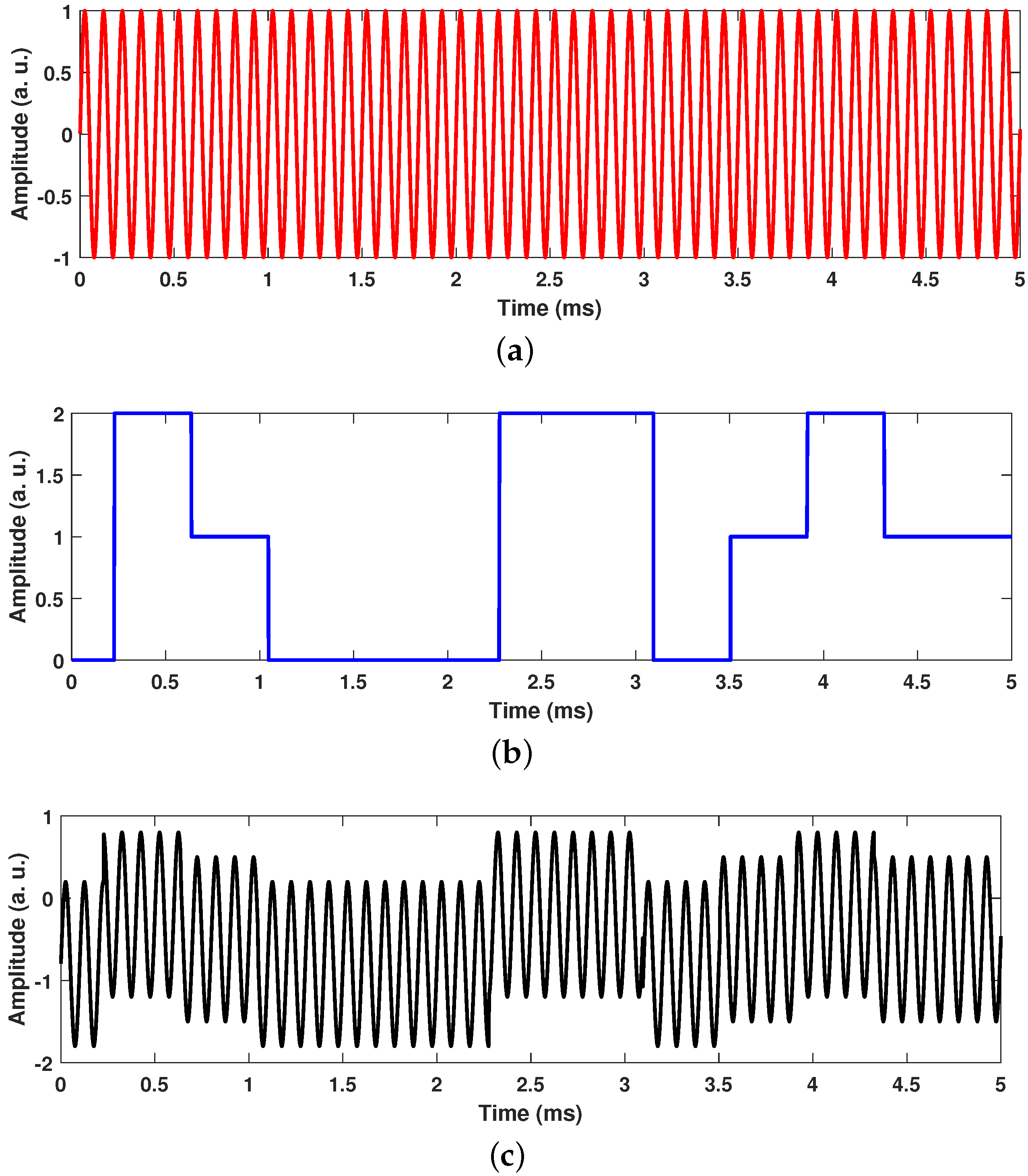
where A m is the modulation amplitude, f m is the modulation frequency, A d is the amplitude of the digital signal and DC is the bias signal. The components of the modulation signal can be observed in Figure 5.
Figure 5 illustrates how the digital signal acts like a DC signal on the sinusoidal modulation. We can observe similar behavioral changes as in the numerical and experimental bifurcation diagrams. In this way, we can dynamically change the behavior of the laser by applying a DC signal. We also know that when modulated at a frequency of 10 kHz, the behavior of the laser is independent of the initial conditions, which would make the gates robust.

3. Results

3.1. Numerical Results

As mentioned in earlier sections, the digital signal causes an offset in the sinusoidal modulation signal, which changes the behavior of the LFDE output. This behavior-dependency allowed us to implement the logic gates. When discretizing the gates, it was taken into account that the natural behavior of the LFDE with the modulation parameters f m = 10 kHz and A m = 1 is period 1. So if the laser reacts in period 1, we have a logical “1” or a logical “0” for any other result.
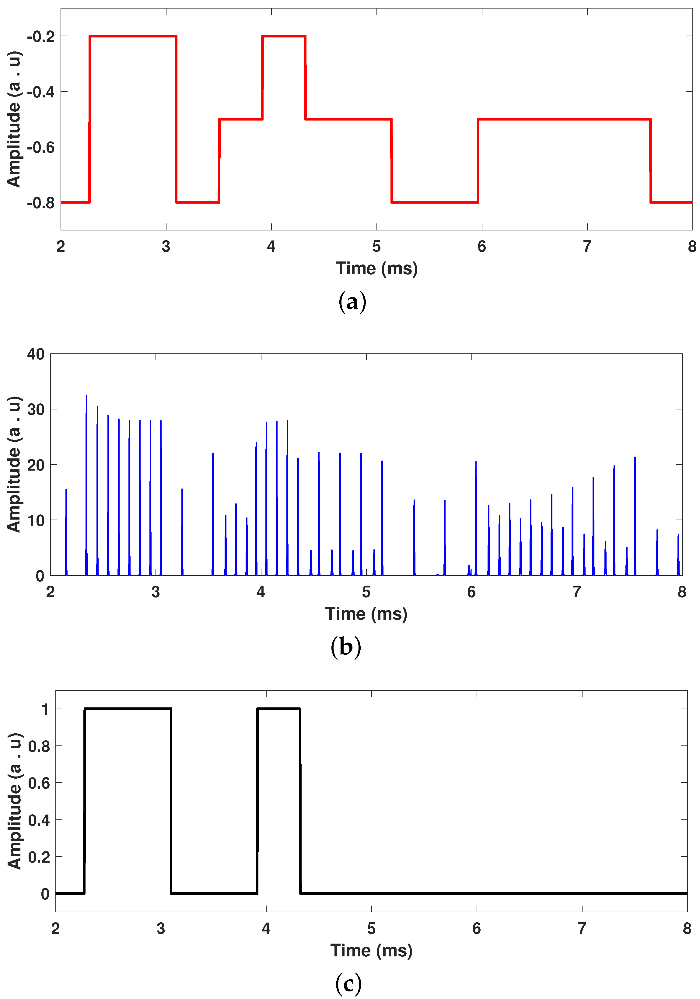
Figure 6a shows the logic input A d ( I 1 + I 2 ) + DC, where A d = 0.3 a.u. and DC = 0.8 a.u., the logic input levels correspond to “0” for the input set (0,0), “1” for the input set (1,0)/(0,1), and “2” for the input set (1,1). Figure 6b corresponds to the laser response, and Figure 6c shows the output of the logic gate. For one set of inputs (1,1), the laser response is P1, and the logic output is “1”, and for any other set of inputs, the behavior of the laser is other than period 1, so the logic output is “0”, which corresponds to the truth table of the AND gate. Using an amplitude of 0.3 a.u. and by varying the DC value, it can obtain logic gates such as AND, OR, NOR, NAND, and XOR, which are shown in Figure 7 and Figure 8.
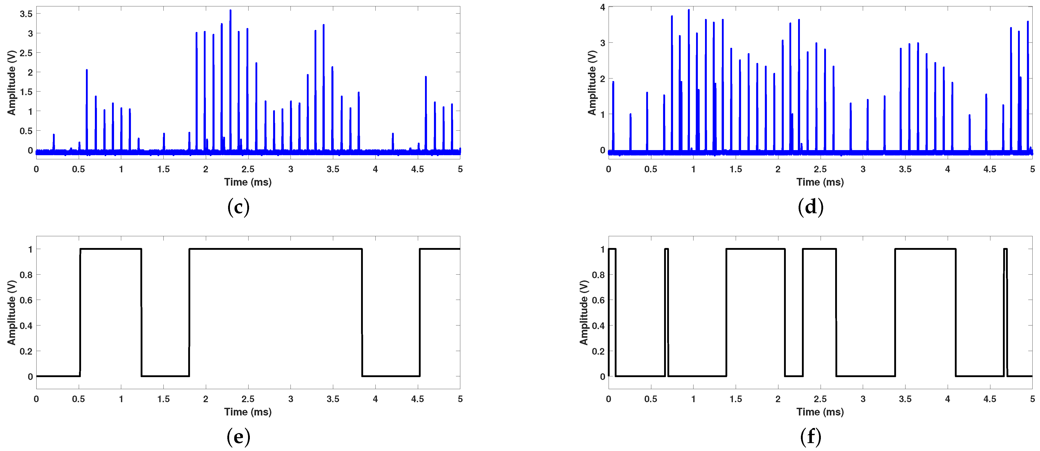
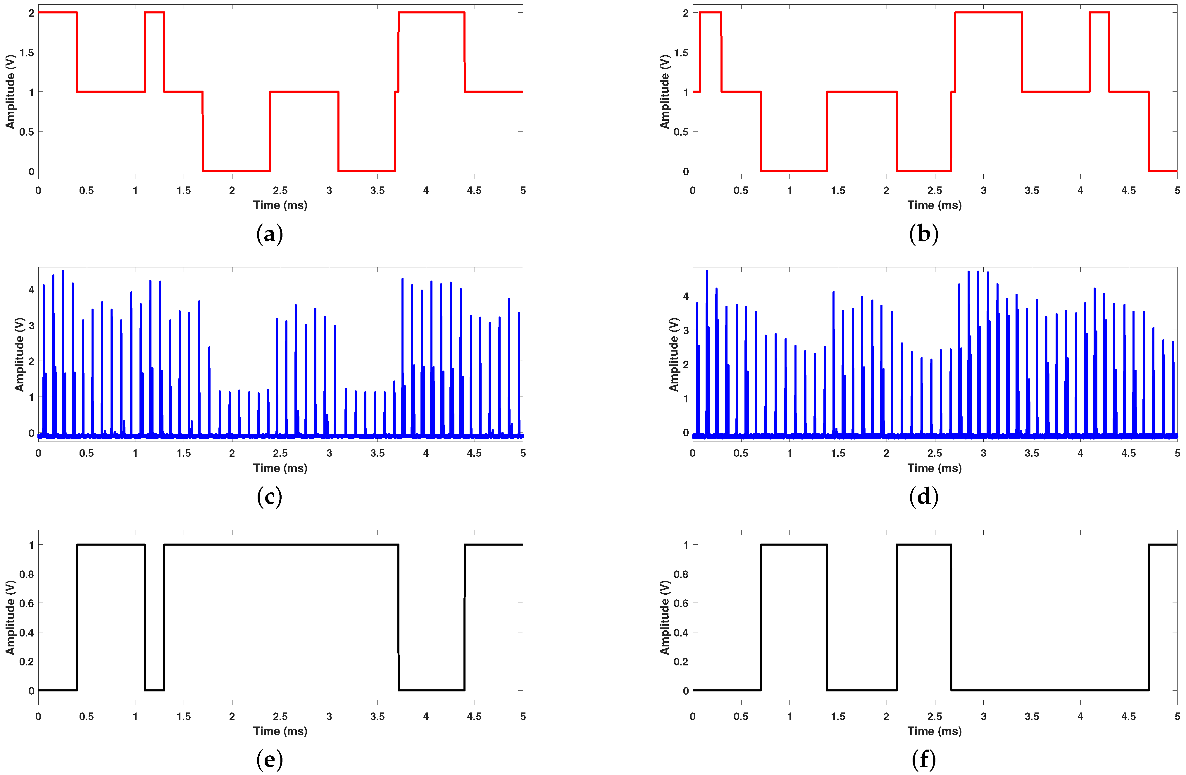
Figure 7 shows the generation of two different logic gates by changing the DC value. The left column shows the signals of a NAND gate, while the right side shows a NOR gate. We believe that the noise referred to by the reviewer is due to the contrast of the colors we use in the figures, which have been modified. The time series shown correspond to the input signal of the logic gate (first row), the response of the laser system in which it has several behaviors on which the logic gate is discretized and built (second row), and the output signal of the logic gate (third row).
The figures shown in Figure 8 show that the laser response as a NAND logic gate. After scanning the values for the DC and the A d , we were able to determine different gates. The relationship between the gates and the parameters is shown in Table 2.
Five logic gates with two inputs are implemented using this method: AND, OR, NOR, NAND, XOR. In Table 2, the combinations where no gate with two inputs could be obtained for these parameters are denoted by N G . For values of A d greater than 0.6 a.u. and for DC > 0.3 a.u., no gates were obtained since the laser intensity for none of the three states has the period 1. The numerical results show that the predominant gate is the XOR gate.

3.2. Experimental Results

Using the same methodology for the numerical implementation, a logical output “1” is defined for a laser signal of period 1, and a logical output “0” for any other type of laser intensity behavior. In this way, we were able to implement five logic gates: AND, OR, XOR, NOR, and NAND. All gates can be implemented for a digital signal amplitude of A d = 0.5 V. These are shown in Figure 9, Figure 10 and Figure 11.
The experimental implementation is similar to the numerical analysis: different logic gates can be implemented by changing the parameters of the digital input signal. The ratio of experimental gates for each set of parameters ( D C , A d ) is shown in Table 3.
We can observe that, in the experimental implementation, the NOR gate predominates, which is due to the characteristics of the system, by increasing the DC signal or the amplitude of the digital signal, which, as in Figure 5 applies a DC signal to the sinusoidal signal, experimentally increases the current, resulting in a laser emission that deviates from the period 1, which is the natural response for a frequency of 10 kHz. This occurs for DC signals greater than A m / 2 . If the DC signal is negative, i.e., greater than A m / 2 , the laser does not emit because the current is below the emission threshold.

4. Discussion

Figure 3 shows that a change in the value of the DC signal causes the laser intensity to change from period 1 to a different behavior. In both numerical and experimental implementations, we observed differences in behavior when a negative DC value and a value greater than the modulation amplitude were used. The amplitude in the intensity shows that the laser has emitted, which was also evident in the time series. However, this was not the case in the experimental diagram. If the DC signal was higher than the modulation, the laser did not emit.
We found that increasing the negative DC value leads to a decrease in the amplitude intensity of the laser while maintaining the period. Both implementations showed this effect. This behavior was essential for our implementation because we can implement different logic gates by changing the states or periods of the laser with a DC signal. In this way, we can determine a relationship between the states of the laser intensity and the logic signal. By entering this relationship, a rule for the logic output is determined. By applying this rule, we can determine the logic gates. In our case, the rule was that the response period for normal laser conditions f m = 10 kHz and A m = 1 V the laser response was period 1, so the output assignment will be logic 1; in any other case, it will be 0. In the numerical and experimental implementation, we can observe that the logic gates match the truth tables, as shown in Table 4.
With this simple discretization rule, it is possible to obtain five reconfigurable logic gates embedded in the optical system. In contrast to other approaches presented in the literature (see Table 5), our scheme can obtain a larger number of logic gates, all reconfigurable by an accessible parameter in the system. Unlike what is presented in references [16,17,20,27], in which they carry out the implementation of the logic gates, their results are limited to theoretical developments, instead our numerical results were experimentally validated. They were developed in a laser emission system with a wavelength used in current telecommunication systems.

5. Conclusions

The results confirmed the implementation of a dynamic logic gate resulting from the variations in the parameters of the digital input signal: the amplitude of the digital signal A d and a bias voltage DC. Five logic gates were obtained in both the experimental and numerical implementation: OR, AND, XOR, NAND, and NOR. These gates were not obtained for the same parameter values because the numerical implementation is considered as noise-free, while the experimental one has intrinsic system noise. To perform the implementation, the period of the states of the digital signal must be given. This must be greater than twice the period of the modulation signal. Otherwise, the period cannot be determined, or the gate may exhibit errors, as was observed with the experimental XOR gate. However, this implementation was robust, as the behavior of the laser at the selected modulation frequency did not depend on the initial conditions.
Implementing reconfigurable logic gates in optical systems, especially in EDFL, offers technological advantages in the telecommunication field, as they emit at the same wavelength currently used for transmitting information, bringing potential benefits in decision-making and data packaging.
In addition, using the monostable region of the erbium-doped fiber system allows for a more significant number of combinations in obtaining logic gates, as it is not limited to the occurrence of bistable states, as is traditionally performed. In addition, the dynamic region of the EDFL used is more stable against disturbances, which translates into more robust logic gates for use in real applications. The result is a reconfigurable optical system that can operate with five different logic gates accessible via a parameter of the experimental system.

Author Contributions

S.M.A.-D.: Conceptualization, Methodology, Validation, Formal Analysis, Investigation, Data curation, Writing—Original Draft. J.L.E.-M.: Conceptualization, Methodology, Validation, Investigation, Writing—Original Draft, Writing—Review and Editing. G.H.-C.: Investigation, Resources, Project Administration. J.H.G.-L.: Investigation, Resources, Project Administration. E.E.L.-M.: Formal Analysis, Validation. R.J.-R.: Formal Analysis, Resources, Writing—Review and Editing, Project administration. All authors have read and agreed to the published version of the manuscript.

Funding

This project was supported by CONAHCYT under project number 320597.

Data Availability Statement

Data are contained within the article.

Acknowledgments

J.L.E.M. thanks CONAHCYT for support (CVU-706850). R.J.R. thanks CONAHCYT for financial support, project No. 320597.

Conflicts of Interest

The authors certify that they have no affiliations with or involvement in any organization or entity with any financial interest (such as honoraria; educational grants; participation in speakers’ bureaus; membership, employment, consultancies, stock ownership, or other equity interest; and expert testimony or patent-licensing arrangements), or non-financial interest (such as personal or professional relationships, affiliations, knowledge or beliefs) in the subject matter or materials discussed in this manuscript.

References

  1. Bostock, G. Programmable Logic Devices: Technology and Applications; McGraw-Hill Companies: New York, NY, USA, 1988. [Google Scholar]
  2. Awschalom, D.; Loss, D. Semiconductor Spintronics and Quantum Computation; Springer Science & Business Media: Berlin/Heidelberg, Germany, 2002. [Google Scholar]
  3. Brown, S.D.; Francis, R.J.; Rose, J.; Vranesic, Z.G. Field-Programmable Gate Arrays; Springer Science & Business Media: Berlin/Heidelberg, Germany, 2012; Volume 180. [Google Scholar]
  4. Ditto, W.L.; Murali, K.; Sinha, S. Chaos computing: Ideas and implementations. Philos. Trans. R. Soc. Math. Phys. Eng. Sci. 2008, 366, 653–664. [Google Scholar] [CrossRef] [PubMed]
  5. Murali, K.; Sinha, S.; Ditto, W.L.; Bulsara, A.R. Reliable logic circuit elements that exploit nonlinearity in the presence of a noise floor. Phys. Rev. Lett. 2009, 102, 104101. [Google Scholar] [CrossRef] [PubMed]
  6. Murali, K.; Rajamohamed, I.; Sinha, S.; Ditto, W.L.; Bulsara, A.R. Realization of reliable and flexible logic gates using noisy nonlinear circuits. Appl. Phys. Lett. 2009, 95. [Google Scholar] [CrossRef]
  7. Murali, K.; Sinha, S.; Bulsara, A.R.; Dari, A.; Ditto, W.L. Noise enhanced logic gates. In Proceedings of the AIP Conference Proceedings, Lake Louise, AB, Canada, 21–24 September 2010; American Institute of Physics: College Park, MD, USA, 2011; Volume 1339, pp. 67–77. [Google Scholar]
  8. Ditto, W.L.; Miliotis, A.; Murali, K.; Sinha, S.; Spano, M.L. Chaogates: Morphing logic gates that exploit dynamical patterns. Chaos Interdiscip. J. Nonlinear Sci. 2010, 20, 037107. [Google Scholar] [CrossRef]
  9. Cafagna, D.; Grassi, G. Chaos-based SR flip–flop via chua’s circuit. Int. J. Bifurc. Chaos 2006, 16, 1521–1526. [Google Scholar] [CrossRef]
  10. Munakata, T.; Sinha, S.; Ditto, W.L. Chaos computing: Implementation of fundamental logical gates by chaotic elements. IEEE Trans. Circuits Syst. Fundam. Theory Appl. 2002, 49, 1629–1633. [Google Scholar] [CrossRef]
  11. Murali, K.; Sinha, S.; Mohamed, I.R. Chaos computing: Experimental realization of NOR gate using a simple chaotic circuit. Phys. Lett. A 2005, 339, 39–44. [Google Scholar] [CrossRef]
  12. Campos-Cantón, I.; Pecina-Sánchez, J.; Campos-Cantón, E.; Rosu, H.C. A simple circuit with dynamic logic architecture of basic logic gates. Int. J. Bifurc. Chaos 2010, 20, 2547–2551. [Google Scholar] [CrossRef]
  13. Diaz-Diaz, I.A.; Campos, E. An Analog Voltage Reconfigurable Logic Gate. In Proceedings of the 2023 IEEE International Autumn Meeting on Power, Electronics and Computing (ROPEC), Ixtapa, Mexico, 18–20 October 2023; Volume 7, pp. 1–5. [Google Scholar]
  14. Murali, K.; Sinha, S.; Kohar, V.; Kia, B.; Ditto, W.L. Chaotic attractor hopping yields logic operations. PLoS ONE 2018, 13, e0209037. [Google Scholar] [CrossRef]
  15. Murali, K.; Sinha, S.; Kohar, V.; Ditto, W.L. Harnessing tipping points for logic operations. Eur. Phys. J. Spec. Top. 2021, 230, 3403–3409. [Google Scholar] [CrossRef]
  16. Singh, K.P.; Sinha, S. Enhancement of “logical” responses by noise in a bistable optical system. Phys. Rev. E Stat. Nonlinear Soft Matter Phys. 2011, 83, 046219. [Google Scholar] [CrossRef] [PubMed]
  17. Perrone, S.; Vilaseca, R.; Masoller, C. Stochastic logic gate that exploits noise and polarization bistability in an optically injected VCSEL. Opt. Express 2012, 20, 22692–22699. [Google Scholar] [CrossRef] [PubMed]
  18. Zhong, D.; Yang, G.; Xiao, Z.; Ding, Y.; Xi, J.; Zeng, N.; Yang, H. Optical chaotic data-selection logic operation with the fast response for picosecond magnitude. Opt. Express 2019, 27, 23357–23367. [Google Scholar] [CrossRef] [PubMed]
  19. Zhong, D.; Yang, G.; Zeng, N.; Yang, H.; Xu, Z.; Xi, J. Optical chaotic flip-flop operations with multiple triggering under clock synchronization in the VCSEL with polarization-preserved optical injection. Opt. Express 2020, 28, 10363–10377. [Google Scholar] [CrossRef] [PubMed]
  20. Shahi, M.; Khatib, F. Design, simulation and optimization of all-optical NOT/XOR logic gates for use in the new photonic crystal 4 × 2 encoder. Int. J. Nonlinear Anal. Appl. 2021, 12, 1035–1045. [Google Scholar]
  21. Mehdizadeh, F.; Soroosh, M. Designing of all optical NOR gate based on photonic crystal. Indian J. Pure Appl. Phys. 2016, 54, 35–39. [Google Scholar]
  22. Moniem, T.A. All-optical digital 4 × 2 encoder based on 2D photonic crystal ring resonators. J. Mod. Opt. 2016, 63, 735–741. [Google Scholar] [CrossRef]
  23. Kouddad, E.; Naoum, R. Optimization of an all-optical photonic crystal NOT logic gate using switch based on nonlinear Kerr effect and ring resonator. Sens. Lett. 2020, 18, 89–94. [Google Scholar] [CrossRef]
  24. Jindal, P.; Abou Houran, M.; Goyal, D.; Choudhary, A. A review of different techniques used to design photonic crystal-based logic gates. Optik 2023, 280, 170794. [Google Scholar] [CrossRef]
  25. Afanador Delgado, S.M.; Echenausía Monroy, J.L.; Huerta Cuellar, G.; García López, J.H.; Reátegui, R.J. Implementation of logic gates in an erbium-doped fiber laser (EDFL): Numerical and experimental analysis. Photonics 2022, 9, 977. [Google Scholar] [CrossRef]
  26. Pisarchik, A.N.; Kir’yanov, A.V.; Barmenkov, Y.O.; Jaimes-Reátegui, R. Dynamics of an erbium-doped fiber laser with pump modulation: Theory and experiment. JOSA B 2005, 22, 2107–2114. [Google Scholar] [CrossRef]
  27. Gupta, N. Logic gates based on optical transistors. J. Opt. Commun. 2024, 44, s367–s377. [Google Scholar] [CrossRef]
  28. Murali, K.; Rajasekar, S.; Aravind, M.V.; Kohar, V.; Ditto, W.; Sinha, S. Construction of logic gates exploiting resonance phenomena in nonlinear systems. Philos. Trans. R. Soc. A 2021, 379, 20200238. [Google Scholar] [CrossRef] [PubMed]
  29. Zhou, Z.; Liu, C.; Fang, Y.; Zhou, J.; Glasser, R.T.; Chen, L.; Jing, J.; Zhang, W. Optical logic gates using coherent feedback. Appl. Phys. Lett. 2012, 101, 191113. [Google Scholar] [CrossRef]
Figure 1. EDFL bifurcation diagram. (a) Numerically calculated, (b) experimentally determined.
Photonics 11 01103 g001
Figure 2. Experimental setup. (a) Optical elements required to put the Erbium-Doped Fiber Laser into operation (b) Elements required to implement the logic gate based on the operation of the EDFL. WFG: Wave Form Generator; LDC: Laser Diode Controller; PD: Photo-Detector; WDM: Wavelength Division Multiplexing; OS: Osciloscope; FBG: Fiber Bragg Grating.
Photonics 11 01103 g002
Figure 3. Bifurcation diagram at a modulation frequency of f m = 10 kHz. (a) Numerically calculated −1 a.u. < DC < 1 a.u., (b) experimentally determined −1 V < DC < 1 V.
Photonics 11 01103 g003
Figure 4. Changes observed in the behavior of laser intensity by adding a DC signal to pump modulation (Numerically calculated on the left, and experimentally observed on the right). Left axis laser amplitude (solid line) and right axis DC amplitude (dash line). Response at DC signal with amplitude (a,b) 0.5 V < DC < 0.9 V, (c,d) 0.1 V < DC < 0.4 V, (e,f) −0.5 V < DC < −0.1 V, (g,h) −0.9 V < DC < −0.6 V.
Photonics 11 01103 g004
Figure 5. Modulation signal. (a) Sinusoidal signal with a frequency f m = 10 kHz and A m = 1 a.u. (b) Sum of the digital signals I 1 + I 2 , with amplitude A d = 1 a.u. (c) Modulation signal A m sin ( 2 π f m t ) + A d ( I 1 + I 2 ) + DC for modulating the laser current, A m = 1 a.u., f m = 10 kHz, A d = 0.3 a.u. and DC = −0.8 a.u.
Photonics 11 01103 g005
Figure 6. Numerical result of the laser operating as an AND logic gate for DC = −0.8 a.u., A d = 0.3 a.u. (a) digital signals fed into the system, (b) temporal behavior of the system when stimulated with the digital signal, (c) output signal of the constructed logic gate.
Photonics 11 01103 g006
Figure 7. Numerically calculated signals of the modulated laser system responding as a logic gate. The left column shows the behavior of the EDFL responding as an OR logic gate ( DC = 0.7 a.u., A d = 0.3 a.u.), while the right column shows the laser system acting as an XOR gate ( DC = 0.5 a.u., A d = 0.3 a.u.). (a,b) Digital input injected into the laser system. (c,d) Laser emission of the system under stimulation of the digital input. (e,f) Response of the logic gate built with the EDFL in monostable regime.
Photonics 11 01103 g007
Figure 8. Dynamic response numerically calculated of the EDFL as a logic gate for different DC values. Left column shows the behavior of the EDFL responding as an NAND gate ( DC = 0.4 a.u., A d = 0.3 a.u.), while the right column shows the laser system acting as an NOR gate ( DC = 0.3 a.u., A d = 0.3 a.u.). (a,b) Digital input injected into the EDFL. (c,d) Laser emission of the system under stimulation of the digital input. (e,f) Response of the logic gate built with the EDFL in monostable regime.
Photonics 11 01103 g008
Figure 9. Experimentally obtained signals of the modulated laser system responding as an AND logic gate for A d = 0.5 V y DC = −0.1 V. (a) Digital input injected into the laser system. (b) Laser emission of the system under stimulation of the digital input. (c) Response of the logic gate built with the EDFL in monostable regime.
Photonics 11 01103 g009
Figure 10. Experimental signals of the modulated laser system responding as a logic gate. The left column shows the behavior of the EDFL responding as an OR logic gate ( A d = 0.5 V , DC = 0 V), while the right column shows the laser system acting as an XOR gate ( A d = 0.5 V , DC = 0.1 V). (a,b) Digital input injected into the laser system. (c,d) Laser emission of the system under stimulation of the digital input. (e,f) Response of the logic gate built with the EDFL in monostable regime.
Photonics 11 01103 g010aPhotonics 11 01103 g010b
Figure 11. Experimental behavior of the modulated EDFL responding as a logic gate. The left column shows the behavior of the EDFL responding as an NAND logic gate ( A d = 0.5 V y DC = 0.2 V), while the right column shows the laser system acting as an NOR gate ( A d = 0.5 V y DC = 0.3 V). (a,b) Digital input injected into the laser system. (c,d) Laser emission of the system under stimulation of the digital input. (e,f) Response of the logic gate built with the EDFL.
Photonics 11 01103 g011
Table 1. Parameters of the normalized system of equations for the EDFL described by Equation (1).
ParameterValueParameterValue
a 6.620 × 10 7 b 7.415 × 10 6
c0.016d 4.076 × 10 3
e506 r w 0.307
ζ 2 r w 0.615 β α 0 L −18
Table 2. The ratio of gates with two inputs. Numerical approximation. The columns represent a change in the amplitude A d of the digital signal, while the rows represent a change in the DC value.
DC (a.u.)/ A d (a.u.)0.10.20.30.40.50.6
−0.8NGANDANDXORXORXOR
−0.7NGANDORXORXORXOR
−0.6ANDORXORXORXORNG
−0.5ORORXORXORNGNG
−0.4NGNANDNANDNORNORNOR
−0.3NGNANDNORNORNORNOR
Table 3. Ratio of 2-input gates. Experimental implementation. The columns represent a change in the amplitude A d of the digital signal, while the rows represent a change in the value DC. For parameter sets (DC(V)/ A d ( V ) ) that cannot implement a logic gate, the NG tag is displayed.
DC(V)/ A d ( V ) 0.20.30.40.50.60.70.80.91.0
−0.5NGNGNGNGNGNORNORNORNOR
−0.4NGNGNGNORNGNORNORNORNOR
−0.3NGNORNORNORNORNORNORNGNG
−0.2NGNANDNANDNANDXORNGNGNGNG
−0.1ORORXORXORXORXORXORXORXOR
0.0ANDANDORORORXORXORXORXOR
0.1NGNGANDANDANDNGNGNGNG
Table 4. Truth tables of the logic gates obtained by numerical and experimental implementation. The middle dash represented a different period than P1.
InputsANDNANDORNORXOR
(0,0)-0P11-0P11-0
(0,1)/(1,0)-0P11P11-0P11
(1,1)P11-0P11-0-0
Table 5. Comparative table of the generation of logic gates based on optical systems.
Reference Logic Gates Reconfigurable Multistable Communications
[16]OR, NOR, AND, NANDYesNoNo
[17]ORNoNoNo
[20]NOT, XORNoNoNo
[21]3-input NORNoNoNo
[27]OR, AND, NOTNoNoNo
[28]OR, AND, NOR, NAND, XNORYesNoNo
[29]OR, NORNoNoYes
[25]NOR, NAND, XNORYesYesYes
This workOR, AND, NOR, NAND, XORYesYesYes
Disclaimer/Publisher’s Note: The statements, opinions and data contained in all publications are solely those of the individual author(s) and contributor(s) and not of MDPI and/or the editor(s). MDPI and/or the editor(s) disclaim responsibility for any injury to people or property resulting from any ideas, methods, instructions or products referred to in the content.