Article

Tunable Optical Filter Based on Thin Film Lithium Niobate Photonic Crystals

1
Institute of Semiconductors, Chinese Academy of Sciences, Beijing 100083, China
2
The College of Materials Science and Opto-Electronic Technology, University of Chinese Academy of Sciences, Beijing 100049, China
*
Author to whom correspondence should be addressed.
Photonics 2024, 11(12), 1134; https://doi.org/10.3390/photonics11121134
Submission received: 4 November 2024 / Revised: 21 November 2024 / Accepted: 29 November 2024 / Published: 2 December 2024
(This article belongs to the Section Optoelectronics and Optical Materials)

Abstract

:
In this paper, we propose a tunable optical filter with a high Q factor based on photonic crystal technology, achieving a Q factor of 442.85 using thin film lithium niobate technology. By proportionally adjusting the dimensions of the unit structure, this filter enables coarse tuning across the 1520–1570 nm range (C band). Furthermore, by utilizing the thermo-optic effect of lithium niobate, we can achieve fine-tuning of the optical filter within a temperature range of 300 K to 600 K, allowing for a center wavelength tuning capability of up to 3.7 nm. This design not only enhances the filter’s performance but also broadens its potential applications in optical communication and optical signal processing.

1. Introduction

Photonic crystals have been extensively researched in recent years due to their advantages of high quality factor (Q factor), compact size, and easy integration. They have emerged as a crucial direction in the advancement of photonic integration technology [1]. The earliest investigations can be traced back to 1970, when Bykov proposed a periodic structure for suppressing specific electromagnetic frequencies [2]. This theory laid the groundwork for subsequent research endeavors. As research deepened, scientists continued exploring various methods to achieve photonic crystal cavities with high quality factors and introduced numerous innovative structural designs. Through the design of different types of periodic structures such as microrings, microdisks, and microspheres, researchers were able to effectively control key performance parameters including sensitivity, bandwidth, and quality factors [3,4,5,6]. Recently, Rose K. Cersonsky et al. discussed the design possibilities of photonic crystals across various material systems and provided a comprehensive dataset on this subject matter [7]. These advancements have led to valuable photonic crystal devices such as broadband sensors with high sensitivity, notch filters with exceptional transmission efficiency, and optical expansion lines for optical signal processing applications [8,9,10,11,12,13]. These devices not only exhibit significant potential in the field of optical communication but also hold promising prospects in diverse areas like biosensing and environmental monitoring. Moving forward, further research on photonic crystals will continue driving innovation and development within photonic integration technology while providing more opportunities for the emergence of next-generation optoelectronic devices.
The tunable filter is a device that highlights the advantages of photonic crystal devices, utilizing the characteristics of photonic crystal structures to achieve selective filtering and tuning of optical signals [14,15,16,17,18,19]. By altering the periodic structure of the photonic crystal or applying external factors such as electric fields and temperature, its optical properties can be adjusted. This type of filter offers high selectivity, tunability, low loss, and compact size, making it valuable in fields such as optical communication, sensors, and optical signal processing [20]. Shaopeng Li et al. tuned the filtering characteristics by adjusting the effective refractive index of the silicon bar and the radius of the filter [21]. However, the flexibility of tuning these material and structural characteristics is limited. To address this, Xiaoling Chen and others proposed a tunable wavelength division multiplexing (WDM) device based on thermally tunable silicon microring resonators, achieving a thermal–optical efficiency of 0.8 mW/FSR with a channel spacing of 50 GHz [22]. With advancements in manufacturing technology and deeper research into photonics, photonic crystal tunable filters are expected to continue evolving towards higher performance, smaller sizes, and broader applications. However, traditional thin film material platforms such as silicon, silica, and silicon nitride [23,24,25,26] have some significant drawbacks, such as limited transparent windows and lower non-linear responses. These issues restrict their applications across a wide spectral range and reduce efficiency in high-power optical modulation and signal processing. In contrast, lithium niobate has a wider transparent window (350–5000 nm) and performs excellently in terms of non-linearity and selectivity [27,28,29,30]. Additionally, thin film lithium niobate possesses outstanding photonic, optoelectronic, and thermoelectric properties, giving it a significant advantage in optical devices and photonic integration [31,32,33]. These characteristics make it a preferred material for various applications, particularly in optoelectronic devices that require high performance and sensitivity [34,35]. Recently, Mingxiao Li and colleagues successfully achieved a high-quality factor photonic cavity mode lithium niobate photonic crystal electro-optic modulator with a tuning efficiency of up to 1.98 GHz V−1 and a modulation bandwidth of 17.5 GHz [36]. This breakthrough not only enhances the performance of lithium niobate photonic crystal devices but also opens new possibilities for future optical communication and information processing technologies.
We propose a high-Q tunable optical filter based on photonic crystals, implemented on a lithium niobate material platform, achieving a quality factor of 442.85. This design not only demonstrates the advantages of high-performance filters but also possesses flexible tunability. To achieve this flexibility, we employed a method that combines altering the periodic structure of the photonic crystal with temperature application. First, by adjusting the periodic structure of the photonic crystal, we can tune the transmission spectrum over a wide range, covering frequencies from 1520 nm to 1570 nm (C band). This strategy enables the filter to effectively meet various application requirements. Subsequently, leveraging the thermal modulation effect of the lithium niobate material, we performed fine-tuning of the transmission spectrum within a narrow range, with a tuning temperature range from 300 K to 500 K. This dual tuning mechanism fully utilizes the advantages of high selectivity, tunability, and low loss, allowing our optical filter to perform exceptionally well in practical applications. Furthermore, creating periodic structures of different sizes within the same device allows for wavelength division multiplexing (WDM) and precise control of the output wavelength through temperature adjustment. This innovative design not only enhances the functionality of the device but also lays a foundation for its extensive application in optical communications and sensors in the future. Such tunable optical filters will promote the development of more efficient and flexible optical signal processing technologies.

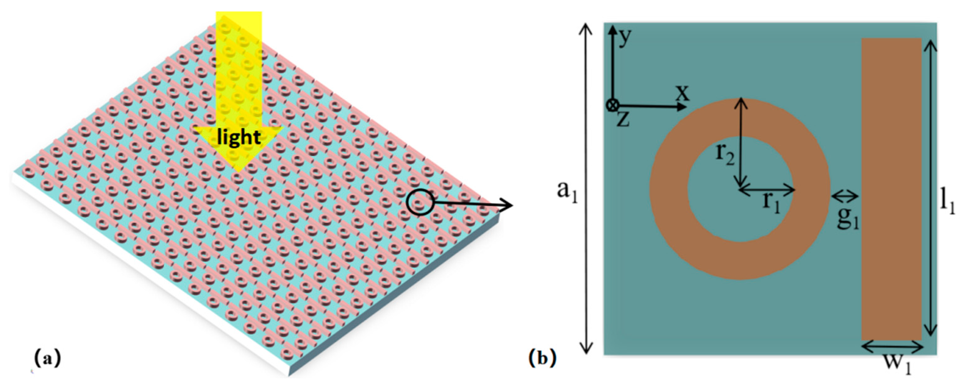
2. Materials and Methods

The schematic diagram of our proposed tunable optical filter is shown in Figure 1a. The optical filter consists of a periodic array of rings and rectangles, both made from thin-film lithium niobate (LiNbO3). The substrate material of the structure is SiO2 with a thickness of 4.7 um. TEM light is incident in the z direction. The coupling of the ring and rectangles structure mode leads to the generation of the resonant mode, which can be optimized through geometric design to achieve the corresponding wavelength and improved quality factor. Our geometric design is shown in Figure 1b, and the detailed parameters mentioned are shown in Table 1. Additionally, the distance between adjacent rectangles is 40 nm.
For the above structures, we carried out a numerical simulation by Lumerical finite-difference time-domain (3D finite element difference). In the model construction, periodic boundary conditions are used in both x and y directions, and a perfect matching layer is used in z direction. In order to increase the accuracy of the simulation results, we conducted a grid setting with a minimum cell of 15 nm and set a long enough running time.

3. Results

In this section, we provide a detailed analysis of the design results and principles, followed by a discussion of two tuning methods.

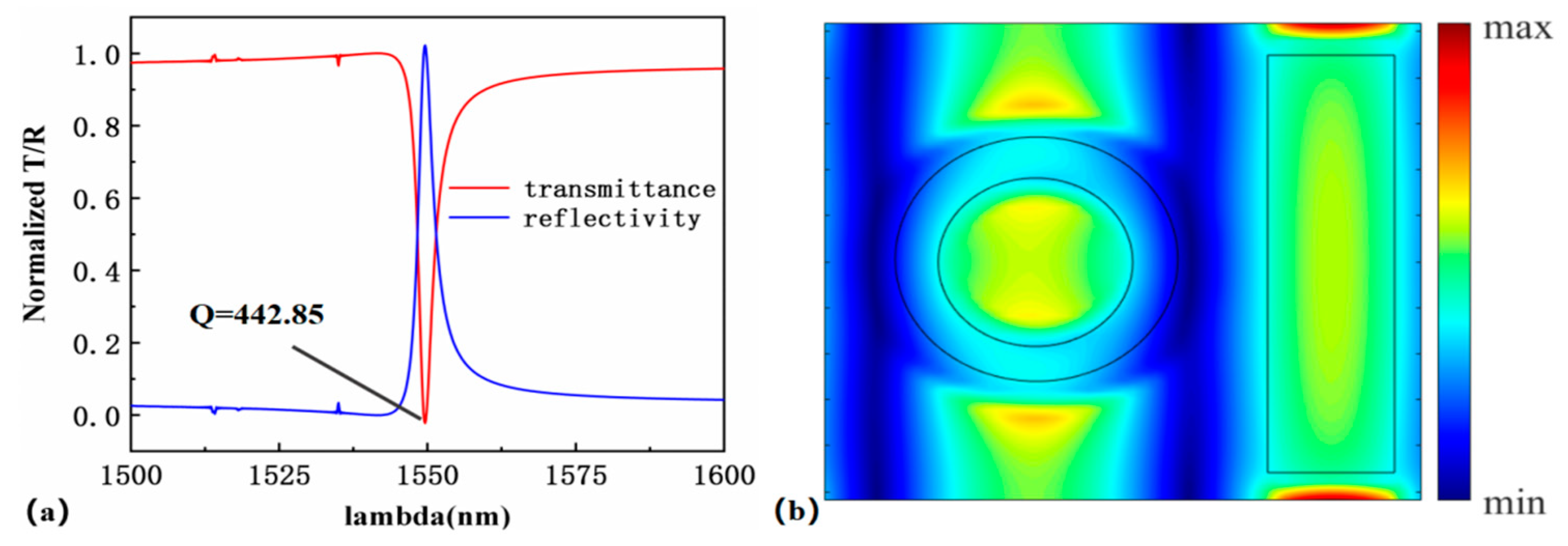
3.1. Results and Analysis of Photonic Crystal Filters

The overall absorption is not obvious, and the simulated transmission and reflection spectrrum are shown in Figure 2a. Under the condition of 1550 nm, a high Q factor resonance peak can be clearly observed, with a Q factor reaching 442.85, indicating good selectivity and sensitivity at this wavelength. Here, we introduce the Q factor to intuitively characterize the performance of the filter. Generally speaking, the quality factor affects the filtering performance of the filter. The narrower the bandwidth, the higher the Q factor of the filter’s resonance, and the better the filtering performance. Its definition is as follows:
Q = f 0 F W H M ,
where f0 is the central wavelength, and FWHM is the full width of the half maximum. Based on its periodic structure and photonic band gap characteristics, the propagation of light is limited and the resonant peak with filtering characteristics is generated. To better understand the physical mechanism of the proposed filter, Figure 2b corresponds to the distribution of the calculated electric field (|Ez| on the z = 0 plane). It can be observed that the electric field is mainly distributed inside and on both sides of the bar structure and the ring, and strong resonance is generated between them, with obvious field enhancement and field–matter interaction.

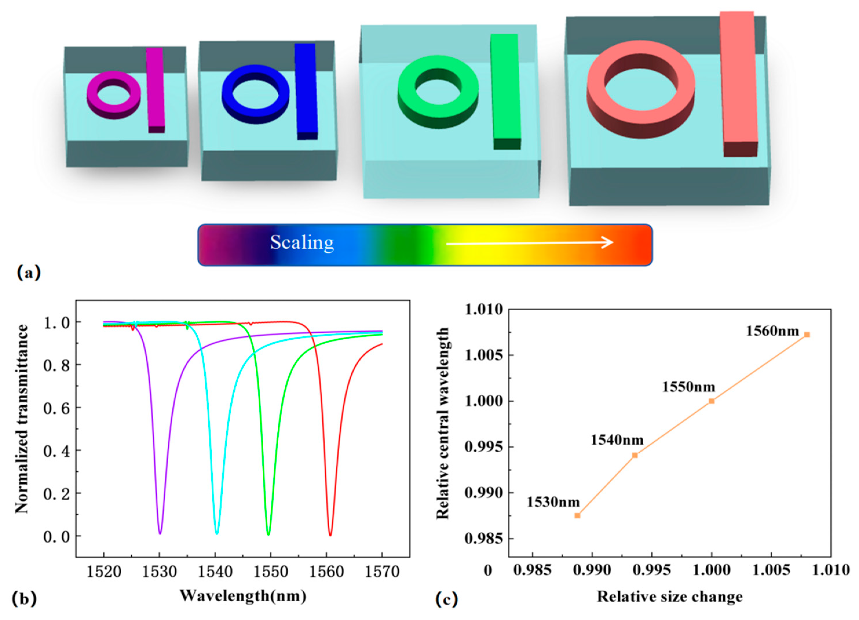
3.2. Analysis of Two Tuning Methods for Photonic Crystal Filters
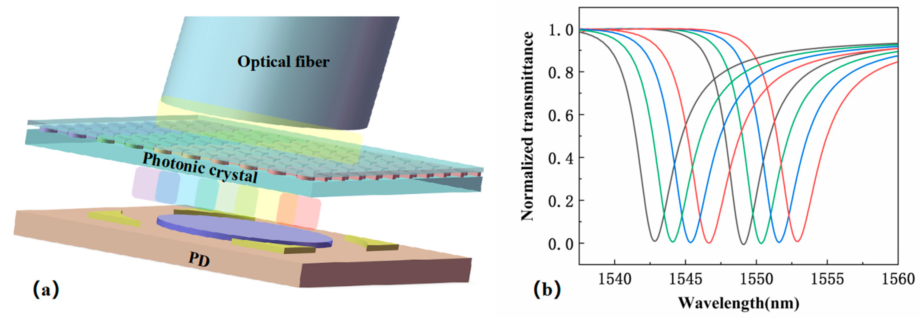
In order to realize the tunability of optical filters, we propose two tuning methods. First, by adjusting the structural parameters of the photonic crystal, such as the position and size of the structure distribution, the resonant wavelength can be controlled to achieve the frequency selectivity and mode characteristics of light. We achieve a rough wide-range tuning by changing the size of the unit structure in equal proportions, as shown in Figure 3a. Figure 3b shows the distribution of transmission spectra under different size unit structures. In the 1520–1570 nm frequency band, the shape of the resonant peak is roughly the same, but the wavelength has changed, showing good tuning characteristics. It can be observed that the corresponding resonance peak redshifts as the size of the unit structure increases in equal proportion. In order to explore the linearity of its change, we plotted the linear distribution of relative size and central wavelength, as shown in Figure 3c. It can be observed that a proportional change in the size of the unit structure can achieve roughly linear tuning.
Second, in order to achieve better wavelength selection, the optical filter is fine-tuned in a small range using the thermo-optical effect of thin film lithium niobate. Figure 4a shows the contrast of periodic structures at different temperatures through different colors. When the temperature of the thin film lithium niobate material is changed in the temperature range of 300 K–600 K, it can be observed that the wavelength of the resonant peak redshifts with the increase of temperature, as shown in Figure 4b. This is because the thermal–optical effect of thin film lithium niobate changes its effective refractive index and realizes the change of wavelength. In the temperature range of 300 K–600 K, the center wavelength can be adjusted to 3.7 nm. In order to better explain the principle, the linear equation of refractive index varying with temperature is used. It is defined as follows:
n ( T ) = n 0 + α ( T T 0 )
where n0 is the primary refractive index, α is the temperature coefficient (=−9.3 × 10−05 K−1), T0 is the reference temperature, and T is the test temperature. According to the formula, the refractive index decreases linearly with the increase of temperature, as shown in Figure 4c. Obviously, the effective refractive index will also be reduced, so that the wavelength can be redshifted. In order to compare the linearity of its wavelength change, we drew a linear distribution diagram of temperature change and central wavelength distribution, as shown in Figure 4d. It can be observed that it exhibits a very good linear change, as we would expect. Large dimensional tuning is difficult to accurately control at a certain wavelength, and small temperature tuning has a limited effective tunable range. The selection of the size can be made prior to manufacturing, and once the structure is determined, it cannot be changed. At this point, temperature tuning can be employed to achieve small-range adjustments. By combining these two tuning methods, we not only achieve more precise wavelength selection, but also introduce greater flexibility into the device.

4. Discussion

We compare different tunable photonic crystal filters as shown in Table 2. Most of the existing work focuses on the individual analysis of size tuning and temperature tuning. However, as mentioned earlier, each method has its limitations. The limitations of dimensional tuning lie in fixed structural design, material constraints, and manufacturing errors. On the other hand, the limitation of temperature tuning is its poor stability. By combining both dimensional and temperature tuning, it is possible to enhance tuning precision while maintaining system stability. Temperature tuning offers precise fine-tuning capabilities, while dimensional tuning provides greater flexibility over a wider range.
In order to better demonstrate the application of this design, we present an application scenario as shown in Figure 5a. It can not only realize simple filtering function, but also be used as surface incident multi-wavelength selective device. In the multi-channel optical transmission, the cycle structure of different sizes is used to achieve multi-wavelength selection through the combination of size and temperature regulation. The resulting central wavelengths for multi-wavelength selective can be controlled by adjusting the size and temperature, as illustrated in Figure 5b. Specifically, the provided image demonstrates the wavelength variation for two different sizes within the temperature range of 300 K to 600 K, highlighting the system’s ability to selectively choose specific wavelengths. Combined with the surface incident detector chip, this design will greatly improve the efficiency and flexibility in practical applications. This innovation not only simplifies the filtering function, but also provides convenience for multi-channel signal processing, and has important application prospects.

5. Conclusions

In our study, we designed an optical filter based on a photonic crystal structure using thin film lithium niobate on insulator, which offers superior optical selectivity due to its high Q factor. We discussed two tunable approaches: one is achieving a wide tuning range (C band) by adjusting the dimensions of the unit structure, and the other is fine-tuning through the thermo-optic effect of lithium niobate on insulator, allowing for a center wavelength tuning range of 3.7 nm within the temperature range of 300 K to 600 K. The combination of dimensional tuning and temperature tuning enables a broader tuning range and higher tuning precision. Additionally, we explored the functionality of this optical filter in multi-wavelength selective for optical communication.

Author Contributions

Conceptualization, L.W. and Z.Z.; methodology, L.W. and T.Y.; software, L.W. and H.F.; validation, L.W., J.L. and Z.Z.; formal analysis, T.Y. and S.Z.; investigation, L.W.; data curation, J.L.; writing—original draft preparation, L.W.; writing—review and editing, Z.Z.; supervision, J.L. All authors have read and agreed to the published version of the manuscript.

Funding

This research received no external funding.

Institutional Review Board Statement

Not applicable.

Informed Consent Statement

Not applicable.

Data Availability Statement

The data presented in this study are available on reasonable request from the corresponding author.

Acknowledgments

Thanks to other people who contributed to the paper but were not mentioned.

Conflicts of Interest

The authors declare no conflicts of interest.

References

  1. Prather, D.W. Photonic Crystal Structures and Applications: Perspective, Overview, and Development. J. Sel. Top. Quantum Electron. 2006, 12, 1416–1437. [Google Scholar] [CrossRef]
  2. Bykov, V. Spontaneous emission in a periodic structure. Sov. J. Exp. Theor. Phys. 1972, 35, 269–273. [Google Scholar]
  3. Ren, L.; Wen, H.; Shi, L.; Zhang, X. Electromagnetically induced transparency with a single optomechanical microring resonator. Opt. Lett. 2022, 47, 1363. [Google Scholar] [CrossRef] [PubMed]
  4. Manjeshwar, S.K.; Elkhouly, K.; Fitzgerald, J.M.; Ekman, M.; Zhang, Y.; Zhang, F.; Wang, S.; Tassin, P.; Wieczorek, W. Suspended photonic crystal membranes in AlGaAs heterostructures for integrated multi-element optomechanics. Appl. Phys. Lett. 2020, 116, 264001. [Google Scholar] [CrossRef]
  5. Benevides, R.; M’enard, M.; Wiederhecker, G.; Alegre, T. Ar/Cl 2 etching of GaAs optomechanical microdisks fabricated with positive electroresist. Opt. Mater Exp. 2020, 10, 57–67. [Google Scholar] [CrossRef]
  6. Xia, J.; Qiao, Q.; Zhou, G.; Chau, F.; Zhou, G. Opto-mechanical photonic crystal cavities for sensing application. Appl. Sci. 2020, 10, 7080. [Google Scholar] [CrossRef]
  7. Cersonsky, R.K.; Antonaglia, J.; Dice, B.D.; Glotzer, S. The diversity of three-dimensional photonic crystals. Nat. Commun 2021, 12, 2543. [Google Scholar] [CrossRef]
  8. Li, M.; Liang, H.; Luo, R.; He, Y.; Lin, Q. High-q 2d lithium niobate photonic crystal slab nanoresonators. Laser Photon. Rev. 2019, 13, 1800228. [Google Scholar] [CrossRef]
  9. Wang, Z.; Yi, S.; Chen, A.; Chen, A.; Zhou, M.; Luk, T.S.; James, A.; Nogan, J.; Ross, W.; Joe, G.; et al. Single-shot on-chip spectral sensors based on photonic crystal slabs. Nat. Commun. 2019, 10, 1020. [Google Scholar] [CrossRef]
  10. Brunetti, G.; Dell’Olio, F.; Conteduca, D.; Armenise, M.; Ciminelli, C. Ultra-compact tuneable notch filter using silicon photonic crystal ring resonator. J. Light. Technol. 2019, 37, 2970–2980. [Google Scholar] [CrossRef]
  11. Zhong, H.; Li, J.; He, Y.; Zhang, R.; Wang, H.; Shen, J.; Zhang, Y.; Su, Y. Ultra-low-power consumption silicon electro-optic switch based on photonic crystal nanobeam cavity. Npj Nanophoton. 2024, 1, 33. [Google Scholar] [CrossRef]
  12. Wang, Y.; Sheng, Y.; Liu, S.; Zhao, R.; Xu, T.; Xu, T.; Chen, F.; Krolikowski, W. Wavelength-dependent nonlinear wavefront shaping in 3D nonlinear photonic crystal. Chin. Opt. Lett. 2024, 22, 071901. [Google Scholar] [CrossRef]
  13. Takahiro, U.; Hisashi, C.; Taiki, Y.; Yuto, M.; Yusuke, T.; Masaaki, O.; Eiichi, K.; Masaya, N. Nanocavity tuning and formation controlled by the phase change of sub-micron-square GST patterns on Si photonic crystals. Opt. Express 2024, 32, 1802–1824. [Google Scholar]
  14. Chen, X.; Zhang, P.; Zhong, D.; Dong, J. Tunable Dual- and Multi-Channel Filter Based on Cantor Photonic Crystals Embedded With Graphene. IEEE Access 2023, 11, 8433–8440. [Google Scholar] [CrossRef]
  15. Lou, B.; Wang, B.; Rodríguez, J.A.; Cappelli, M.; Fan, S. Tunable guided resonance in twisted bilayer photonic crystal. Sci. Adv. 2022, 8, 4339. [Google Scholar] [CrossRef] [PubMed]
  16. Chettah, C.; Barkat, O.; Chaabi, A. Tunable Properties of Optical Selective Filters Based on One-Dimensional Plasma Superconductor Photonic Crystal. J. Supercond. Nov. Magn. 2021, 34, 2239–2248. [Google Scholar] [CrossRef]
  17. Park, W.; Park, H.; Choi, Y.-S.; Yoon, D. Optical Rotation-Based Tunable Color Filter Using Chiral Photonic Crystal. Adv. Opt. Mater. 2022, 10, 2201. [Google Scholar] [CrossRef]
  18. Cheng, S.; Li, W.; Zhang, H.; Majid, N.; Yi, Z.; Zeng, Q.; Ma, C.; Sun, T.; Wu, P. High sensitivity five band tunable metamaterial absorption device based on block like Dirac semimetals. Opt. Commun. 2024, 569, 130816. [Google Scholar] [CrossRef]
  19. Li, W.; Cheng, S.; Zhang, H.; Yi, Z.; Tang, B.; Ma, C.; Wu, P.; Zeng, Q.; Raza, R. Multi-Functional Metasurface: Ultra-Wideband/Multi-Band Absorption Switching by adjusting Guided Mode Resonance and Local Surface Plasmon Resonance Effects. Commun. Theor. Phys. 2024, 76, 065701. [Google Scholar] [CrossRef]
  20. Aigner, A.; Weber, T.; Wester, A.; Stefan, A.M.; Andreas, T. Continuous spectral and coupling-strength encoding with dual-gradient metasurfaces. Nat. Nanotechnol. 2024. Online ahead of print. [Google Scholar] [CrossRef]
  21. Li, S.; Liu, H.; Sun, Q.; Huang, N. A Tunable Terahertz Photonic Crystal Narrow-Band Filter IEEE Photon. Technol. Lett. 2015, 27, 752–754. [Google Scholar] [CrossRef]
  22. Chen, X.; Gu, M.; Chen, J.; Wang, S.; Wang, D.; Wang, W.; Zeng, Y.; Chen, H.; Yu, M.; Fang, Q. Low-power and tunable silicon-photonics micro-ring WDM device with NiSi heater. Optik. Volume 2021, 245, 167624. [Google Scholar] [CrossRef]
  23. Liu, W.; Li, M.; Guzzon, R.S.; Norberg, E.; Parker, J.; Lu, M.; Coldren, L.; Yao, J. A fully reconfigurable photonic integrated signal processor. Nat. Photonics 2016, 10, 190–195. [Google Scholar] [CrossRef]
  24. Nagarajan, R.; Kato, M.; Lambert, D.; Evans, P.; Corzine, S.; Lal, V.; Rahn, J.; Nilsson, A.; Fisher, M.; Kuntz, M. Terabit/s class InP photonic integrated circuits Semicond. Sci. Technol. 2012, 27, 094003. [Google Scholar]
  25. Junqiu, L.; Lucas, E.; Rasa, A.S.; He, J.; Riemensberger, J.; Wang, R.; Karpov, M.; Guo, H.; Bouchand, R.; Kippenberg, T.J. Photonic microwave generation in the X- and K-band using integrated soliton microcombs. Nat. Photonics 2020, 14, 486–491. [Google Scholar]
  26. Sacher, W.D.; Huang, Y.; Lo, G.-Q.; Poon, J.K.S. Multilayer silicon nitride-on-silicon integrated photonic platforms and devices. J. Lightwave Technol. 2015, 33, 901–910. [Google Scholar] [CrossRef]
  27. Ge, R.; Yan, X.; Liang, Z.; Li, H.; Wu, J.; Liu, X.; Chen, Y.; Chen, X. Large quality factor enhancement based on cascaded uniform lithium niobate bichromatic photonic crystal cavities. Opt. Lett. 2023, 48, 113–116. [Google Scholar] [CrossRef]
  28. Witmer, J.D.; Hill, J.T.; Safavi-Naeini, A.H. Design of nanobeam photonic crystal resonators for a silicon-on-lithium-niobate platform. Opt. Express 2016, 24, 5876–5885. [Google Scholar] [CrossRef]
  29. Lu, J.; Zhou, S.; Wu, Y.; Yu, H. Two-dimensional thin film lithium niobate photonic crystal waveguide for integrated photonic chips. Appl. Phys. Lett. 2024, 124, 141104. [Google Scholar] [CrossRef]
  30. Chen, D.; Muhammad, S.; Huang, W.; Zheng, X.; Wen, G.; Huang, Y. Parameter investigations on lithium-niobate-based photonic crystal optomechanical cavity. Results Phys. 2023, 48, 2211–3797. [Google Scholar] [CrossRef]
  31. Shi, C.; Yuan, J.; Luo, X.; Shi, S.; Lu, S.; Yuan, P.; Xu, W.; Chen, Z.; Yu, H. Transmission characteristics of multi-structure bandgap for lithium niobate integrated photonic crystal and waveguide. Opt. Commun. 2020, 461, 125222. [Google Scholar] [CrossRef]
  32. Lin, J.; Bo, F.; Cheng, Y.; Xu, J. Advances in on-chip photonic devices based on lithium niobate on insulator. Photon. Res. 2020, 8, 1910–1936. [Google Scholar] [CrossRef]
  33. Leng, R.; Chen, X.; Liu, P.; Zhu, Z.; Zhang, J. High Q lithium niobate metasurfaces with transparent electrodes for efficient amplitude and phase modulation. Appl. Opt. 2024, 63, 3156–3161. [Google Scholar] [CrossRef] [PubMed]
  34. Zhang, Q.; Li, M.; Xu, J.; Lin, Z.; Yu, H.; Wang, M.; Fang, Z.; Cheng, Y.; Gong, Q.; Li, Y. Reconfigurable directional coupler in lithium niobate crystal fabricated by three-dimensional femtosecond laser focal field engineering. Photon. Res. 2019, 7, 503–507. [Google Scholar] [CrossRef]
  35. Rambu, A.P.; Apetrei, A.M.; Doutre, F.; Tronche, H.; Tiron, V.; de Micheli, M.; Tascu, S. Lithium niobate waveguides with high-index contrast and preserved nonlinearity fabricated by a high vacuum vapor-phase proton exchange. Photon. Res. 2020, 8, 8–16. [Google Scholar] [CrossRef]
  36. Li, M.; Ling, J.; He, Y.; Javid, U.A.; Xue, S.; Lin, Q. Lithium niobate photonic-crystal electro-optic modulator. Nat. Commun 2020, 11, 4123. [Google Scholar] [CrossRef]
  37. Li, M.; Liang, H.; Luo, R.; He, Y.; Ling, J.; Lin, Q. Photon-Level Tuning of a High-Q Lithium Niobate Photonic Crystal Nanocavity. In Proceedings of the 2019 CLEO, San Jose, CA, USA, 5–10 May 2019; pp. 1–2. [Google Scholar]
  38. Ji, W.; Gong, Z.; Yin, R.; Li, J.; Li, J.; Lv, L.; Huang, Q. Tunable arrayed waveguide grating optical filter based on lithium niobate-on-insulator and electro-optic effect. Opt. Eng. 2018, 57, 077102. [Google Scholar] [CrossRef]
Figure 1. Schematic diagram of the proposed structure. (a) Periodic distribution structure diagram. (b) Unit structure detailed parameter design drawing.
Photonics 11 01134 g001
Figure 2. (a) The reflection (blue curve) and transmission (red curve) spectra of the filter structure. (b) Electric field intensity distribution corresponding to resonant wavelength.
Photonics 11 01134 g002
Figure 3. (a) Schematic diagram of equal scale changes in cell structure. (b) The distribution of the transmission spectrum with the change of size in the C-band range (the color corresponds to the size change). (c) Image of linear relationship between wavelength and size change (the relative size refers to the ratio of the structure’s dimensions at the labeled wavelength to those at 1550 nm).
Photonics 11 01134 g003
Figure 4. (a) Different colors show the contrast of periodic structures at different temperatures (the actual structural temperature is the same for each cycle). (b) The distribution of the transmission spectrum in the temperature range of 300 K–600 K. (c) The refractive index (1550 nm) decreases linearly with the increase of temperature. (d) shows the linear distribution of temperature change and central wavelength.
Photonics 11 01134 g004
Figure 5. (a) The combination of different size periodic structure and detector chip realizes wavelength division multiplexing. (b) The normalized transmittance image combining two tuning modes (temperature change under two sizes, where the black curve: 300 K, green curve: 400 K, blue curve: 500 K, red curve: 600 K).
Photonics 11 01134 g005
Table 1. Relevant parameters of the designed structure.
ParametersValue (nm)
cycle length (a1)1040
inside diameter of ring (r1)150
outside diameter of ring (r2)310
length of bar (l1)1000
width of bar (w1)200
gap (g1)90
thickness (t)150
Table 2. Comparison of different tunable photonic crystal filters.
MaterialsTuning MethodsWavelength RangeQ Factor
silicon [21]size changes239 um–315 um621.6
silicon [22]temperature changes1552 nm–1562 nm-
lithium niobate [37]input optical power1564 nm–1565 nm1.41 × 106
lithium niobate [38]size changes1548 nm–1555 nm-
lithium niobate [this work]size changes, temperature changes1520 nm–1570 nm442.85
Disclaimer/Publisher’s Note: The statements, opinions and data contained in all publications are solely those of the individual author(s) and contributor(s) and not of MDPI and/or the editor(s). MDPI and/or the editor(s) disclaim responsibility for any injury to people or property resulting from any ideas, methods, instructions or products referred to in the content.

